EP0218372A1 - Vorrichtung zur Herstellung eines thermischen Bildes - Google Patents
Vorrichtung zur Herstellung eines thermischen Bildes Download PDFInfo
- Publication number
- EP0218372A1 EP0218372A1 EP86306856A EP86306856A EP0218372A1 EP 0218372 A1 EP0218372 A1 EP 0218372A1 EP 86306856 A EP86306856 A EP 86306856A EP 86306856 A EP86306856 A EP 86306856A EP 0218372 A1 EP0218372 A1 EP 0218372A1
- Authority
- EP
- European Patent Office
- Prior art keywords
- array
- elements
- resistor
- thermal image
- bus
- Prior art date
- Legal status (The legal status is an assumption and is not a legal conclusion. Google has not performed a legal analysis and makes no representation as to the accuracy of the status listed.)
- Granted
Links
- 230000004907 flux Effects 0.000 claims abstract description 15
- 238000003491 array Methods 0.000 claims description 3
- 238000001816 cooling Methods 0.000 claims description 2
- 239000003989 dielectric material Substances 0.000 claims description 2
- 239000000758 substrate Substances 0.000 abstract description 17
- 239000010409 thin film Substances 0.000 abstract description 3
- 239000010410 layer Substances 0.000 description 13
- 239000004642 Polyimide Substances 0.000 description 4
- 229920001721 polyimide Polymers 0.000 description 4
- 230000008901 benefit Effects 0.000 description 3
- 239000003990 capacitor Substances 0.000 description 3
- 239000011159 matrix material Substances 0.000 description 3
- 230000004048 modification Effects 0.000 description 3
- 238000012986 modification Methods 0.000 description 3
- 230000004044 response Effects 0.000 description 3
- 230000001052 transient effect Effects 0.000 description 3
- IJGRMHOSHXDMSA-UHFFFAOYSA-N Atomic nitrogen Chemical compound N#N IJGRMHOSHXDMSA-UHFFFAOYSA-N 0.000 description 2
- 238000009835 boiling Methods 0.000 description 2
- 238000010586 diagram Methods 0.000 description 2
- ZOKXTWBITQBERF-UHFFFAOYSA-N Molybdenum Chemical compound [Mo] ZOKXTWBITQBERF-UHFFFAOYSA-N 0.000 description 1
- XUIMIQQOPSSXEZ-UHFFFAOYSA-N Silicon Chemical compound [Si] XUIMIQQOPSSXEZ-UHFFFAOYSA-N 0.000 description 1
- RTAQQCXQSZGOHL-UHFFFAOYSA-N Titanium Chemical compound [Ti] RTAQQCXQSZGOHL-UHFFFAOYSA-N 0.000 description 1
- 230000006978 adaptation Effects 0.000 description 1
- 230000008859 change Effects 0.000 description 1
- 230000003111 delayed effect Effects 0.000 description 1
- 230000000694 effects Effects 0.000 description 1
- 238000005530 etching Methods 0.000 description 1
- 238000009413 insulation Methods 0.000 description 1
- 239000007788 liquid Substances 0.000 description 1
- 229910052751 metal Inorganic materials 0.000 description 1
- 239000002184 metal Substances 0.000 description 1
- 238000000034 method Methods 0.000 description 1
- 229910052750 molybdenum Inorganic materials 0.000 description 1
- 239000011733 molybdenum Substances 0.000 description 1
- 229910052757 nitrogen Inorganic materials 0.000 description 1
- 238000001020 plasma etching Methods 0.000 description 1
- 230000005855 radiation Effects 0.000 description 1
- 238000007493 shaping process Methods 0.000 description 1
- 229910052710 silicon Inorganic materials 0.000 description 1
- 239000010703 silicon Substances 0.000 description 1
- 239000002344 surface layer Substances 0.000 description 1
- 239000010936 titanium Substances 0.000 description 1
- 229910052719 titanium Inorganic materials 0.000 description 1
Images



Classifications
-
- B—PERFORMING OPERATIONS; TRANSPORTING
- B41—PRINTING; LINING MACHINES; TYPEWRITERS; STAMPS
- B41J—TYPEWRITERS; SELECTIVE PRINTING MECHANISMS, i.e. MECHANISMS PRINTING OTHERWISE THAN FROM A FORME; CORRECTION OF TYPOGRAPHICAL ERRORS
- B41J2/00—Typewriters or selective printing mechanisms characterised by the printing or marking process for which they are designed
- B41J2/315—Typewriters or selective printing mechanisms characterised by the printing or marking process for which they are designed characterised by selective application of heat to a heat sensitive printing or impression-transfer material
- B41J2/32—Typewriters or selective printing mechanisms characterised by the printing or marking process for which they are designed characterised by selective application of heat to a heat sensitive printing or impression-transfer material using thermal heads
- B41J2/35—Typewriters or selective printing mechanisms characterised by the printing or marking process for which they are designed characterised by selective application of heat to a heat sensitive printing or impression-transfer material using thermal heads providing current or voltage to the thermal head
- B41J2/355—Control circuits for heating-element selection
-
- F—MECHANICAL ENGINEERING; LIGHTING; HEATING; WEAPONS; BLASTING
- F41—WEAPONS
- F41J—TARGETS; TARGET RANGES; BULLET CATCHERS
- F41J2/00—Reflecting targets, e.g. radar-reflector targets; Active targets transmitting electromagnetic or acoustic waves
- F41J2/02—Active targets transmitting infrared radiation
-
- G—PHYSICS
- G01—MEASURING; TESTING
- G01R—MEASURING ELECTRIC VARIABLES; MEASURING MAGNETIC VARIABLES
- G01R31/00—Arrangements for testing electric properties; Arrangements for locating electric faults; Arrangements for electrical testing characterised by what is being tested not provided for elsewhere
- G01R31/28—Testing of electronic circuits, e.g. by signal tracer
- G01R31/302—Contactless testing
Definitions
- U.K. Patent Specification No. 2117957 discloses a thermal image generating device for use in developing and testing infra-red radiation sensitive electro-optical equipment, the device comprising a substrate supporting an array of resistor elements which are able to be selectively heated by the passage of electrical current therethrough so as to produce, from the array, a controllable thermal image made up of pixels which correspond to respective ones of the resistor elements.
- a heat sink is provided to receive and dissipate the heat produced by the resistors.
- a problem with such a device is that, since the temperatures of the elements are not all the same (this must be so as to produce an image), the heat flux flowing into the heat sink is not spatially uniform and, since a fixed image, the heat flux flowing into the heat sink at one point on its surface will also vary with time.
- An object of the invention is to provide a thermal image generating device comprising a resistor array from which the produced heat flux is at least more spatially and temporarily uniform.
- a thermal image producing device comprising an array of first and second resistor elements and electrical current supply means connected to the elements for enabling them to be selectively heated by the passage of electrical current therethrough, the elements being arranged such that heat produced by the first elements is receivable from the device as a controllably variable thermal image while the heat produced by the second elements renders the distribution of the heat flux produced by all the elements substantially uniform over the area of the array.
- a thermal image producing device comprising a first planar array of resistor elements, electrical current supply means connected to the elements of the first array for enabling them them to be selectively heated by the passage of current therethrough and thereby to produce a controllably variable thermal image at one side of the array, a second planar array of resistor elements positioned at the other side of the first array with each element of the second array adjacent a respective corresponding one of the elements of the first array but insulated from said respective corresponding one element of the first array, and from said one side of the first array, by dielectric material; and cooling means for receiving heat from the said other side of the first array and from said second array, the electrical current supply means being further connected to the elements of the second array for enabling them to be selectively heated by the passage of current therethrough to render the distribution of the heat flux produced by all the elements substantially uniform over the area of the arrays.
- the device shown in drawing Figure 4 of UK Patent Specification No. 2117959 comprises a two-dimensional planar array of thin-film resistors mounted on respective dielectric portions which are in turn mounted on a substrate with a bus-bar structure arranged between the dielectric portions and the substrate.
- the bus-bar structure comprises a matrix of column and row bus-bars, each resistor being connected between one row and, via a series diode, one column bus-bar.
- bus-bars are used to address and control the potentials stored on a matrix of capacitors which, in turn, control the currents flowing through respective ones of the resistor elements.
- the capacitors thus act as latching elements which maintain the temperatures of the resistor elements between successive updates thereof.
- each resistor element which forms part of the image producing array i.e. for each 'emitter' resistor
- the resistors are independently addressed so that the total power dissipated is constant: this is controlled by the external drive electronics.
- the compensation technique gives the following advantages:
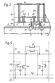
- the image generating device of figures 1 to 4 comprises a deeply finned Molybdenum heatsink 1 supporting a silicon substrate 2.
- the substrate supports a structure including a series of parallel row bus-bars 3, a series of parallel column bus-bars 4 and 5 which are orthogonal to the row bus-bars so that the bus-bars form a matrix, and two arrays of thin-film resistors 6 and 7.
- the resistors 6 are exposed at the outer surface of the structure and are used to produce the thermal image. They are connected to respective ones of the column bus-bars 4 and, via a respective diode 8, to a respective one of the row bus-bars 3.
- the resistors 6 can be selectively addressed and heated by the passage of electrical current therethrough to produce the required image.
- the resistors 7 lie beneath respective ones of the resistors 6, separated tberfrom by an insulation layer 9 of Polymide, and are each connected between that respective column bus-bar 5 which is adjacent to the bus-bar 4 connected to the overlying resistor 6 and, via a diode 10, to the respective bus-bar 3 coupled to that overlying resistor 6.
- the resistors 7 can also be selectively addressed and supplied with electrical current.
- the substrate 2 is provided with a surface layer 11 of oxide dielectric and the diodes 8 and 10 are integrated into the substrate.
- the row bus-bars 3 are deposited on layer 11.
- an aperture 12 is provided in the row bus-bar and two connection pads 13 and 14 are provided on layer 11 within the aperture.
- each diode might be fabricated, in an epitaxial n layer grown on a p substrate, within a reverse-biassed 'bucket diode' formed by an encircling p region and the underlying p substrate, the function of the bucket diode being to electrically isolate the diodes 8 and the diodes 10 one from another.
- Each diode 8 and 10 could have a central anode contact and several cathode contacts around it. Then, of course, the detail geometry of the pads and row bus-bars will need appropriate adaptation from what is shown in figure 3.
- First and second relatively thin layers 16 and 17 of polyimide are deposited over the bus-bars 3, pads 13 and 14 and oxide layer 11 and the much thicker polyimide layer 9 is provided over the layers 16 and 17.
- the column bus-bars 4 and 5 are formed on the first Polyimide layer 16 along with, for each pair of resistors 6 and 7, two connection tags 18 and 19 which connect by way of 'vias' 20 and 21 respectively (through-connections - for example plated-through holes as shown) to respective ones of the pads 13 and 14.
- the resistors 6 and 7, formed by etching of respective layers of titanium, are provided on the outer surfaces of respective ones of the Polyimide layers 9 and 17.
- the holes for the vias 20 to 25 could be formed by plasma etching.
- the raw bus-bars 3 are connected by way of respective amplifiers 26 to respective ones of a series of row selection output terminals 27 of a control circuit 28 which has two further output terminals 29 and 30 connected to respective ones of a gating arrangement 31 and a buffer store 32.
- Image signals say from an image frame store fed by a t.v. camera (not shown) viewing a scene to be reproduced as an image or from an image generating computer (not shown), are received by gating arrangement 31 and, on command from control circuit 28, are passed onto the buffer store 32 to update its content.
- the function of the buffer store is to allow for the likelihood that the frame update rate of the image signal providing apparatus, ie the t.v.
- the buffer store content may be updated via the gating arrangement 31 at the frame rate of the signal providing apparatus, say every 25 milliseconds, and then read out from the buffer store 32 to control the image generator many times within each 25 millisecond period.
- the content of store 32 is read, row-by-row, into a register 33.
- Each digital pixel signal of the raw held in the register 33 is fed to a respective one of a plurality of devices 34, one for each of the column bus-bars 4 and 5, which produce respective resistor drive currents corresponding to the digital pixel signals.
- the drive currents are fed via amplifiers 35 to the column bus-bars 4 and 5.
- the circuit 28 applies a potential, via the appropriate one of its terminal 27 and the associateed amplifier 26, only to the row bus-bar 3 which corresponds to the image pixel row held in the register 33 so as to turn on the diodes 8 and 10 connected to that row bus-bar.
- the potential on the other row bus-bars at this time is made such as to keep the diodes connected thereto turned off.
- the resistors 6 and 7 of the corresponding image generating array row pass the respective drive currents, ie this row is updated.
- the next image signal row is read into the register 33 and the corresponding next row bus-bar has the diode turn on potential applied thereto.
- the sequence is repeated. As noted, the sequence of updating the generated thermal image may occur many times for each update of the image frame held in the buffer store 32.
- Each pixel circuit connects to a corresponding row bus-bar 50 and two column bus-bars 51 and 52 as before, but now also receives drive power from drive rails 53 and 54.
- the emitter resistor 65f is connected between rail 53 and the collector of transistor 56 of which the base is connected to be controlled by the potential stored on capacitor 57. That potential is in turn updated, each time the row bus-bar is strobed, by the signal applied via transistor 58 from column bus-bar 51.
- a similar circuit controls the current flowing through the campensating resistor 7.
- the signal to R 7 can be delayed by a time equivalent to the response of R 6 .
- a simple first order electronic filter incorporated at each pixel would suffice to do this. It may also be possible to incorporate this response shaping in the signal handling external to the device.
- campensating resistors running at constant power eases the design of the drive electronics: with the prior art device to drive the device it may be necessary to have the electronics dump the compensating power into dummy loads.
Landscapes
- Engineering & Computer Science (AREA)
- General Engineering & Computer Science (AREA)
- Physics & Mathematics (AREA)
- Remote Sensing (AREA)
- Electromagnetism (AREA)
- Radar, Positioning & Navigation (AREA)
- General Physics & Mathematics (AREA)
- Transforming Light Signals Into Electric Signals (AREA)
- Cathode-Ray Tubes And Fluorescent Screens For Display (AREA)
- Photographic Developing Apparatuses (AREA)
- Heating, Cooling, Or Curing Plastics Or The Like In General (AREA)
- Printers Or Recording Devices Using Electromagnetic And Radiation Means (AREA)
- Electronic Switches (AREA)
- Non-Silver Salt Photosensitive Materials And Non-Silver Salt Photography (AREA)
Priority Applications (1)
| Application Number | Priority Date | Filing Date | Title |
|---|---|---|---|
| AT86306856T ATE59482T1 (de) | 1985-09-04 | 1986-09-04 | Vorrichtung zur herstellung eines thermischen bildes. |
Applications Claiming Priority (2)
| Application Number | Priority Date | Filing Date | Title |
|---|---|---|---|
| GB8521931 | 1985-09-04 | ||
| GB858521931A GB8521931D0 (en) | 1985-09-04 | 1985-09-04 | Thermal image producing device |
Publications (2)
| Publication Number | Publication Date |
|---|---|
| EP0218372A1 true EP0218372A1 (de) | 1987-04-15 |
| EP0218372B1 EP0218372B1 (de) | 1990-12-27 |
Family
ID=10584688
Family Applications (1)
| Application Number | Title | Priority Date | Filing Date |
|---|---|---|---|
| EP86306856A Expired - Lifetime EP0218372B1 (de) | 1985-09-04 | 1986-09-04 | Vorrichtung zur Herstellung eines thermischen Bildes |
Country Status (5)
| Country | Link |
|---|---|
| US (1) | US4769527A (de) |
| EP (1) | EP0218372B1 (de) |
| AT (1) | ATE59482T1 (de) |
| DE (1) | DE3676618D1 (de) |
| GB (1) | GB8521931D0 (de) |
Cited By (1)
| Publication number | Priority date | Publication date | Assignee | Title |
|---|---|---|---|---|
| WO2004099706A1 (en) * | 2003-05-09 | 2004-11-18 | Saab Ab | Target device |
Families Citing this family (19)
| Publication number | Priority date | Publication date | Assignee | Title |
|---|---|---|---|---|
| US4859080A (en) * | 1988-07-22 | 1989-08-22 | Ssg, Inc. | Dynamic thermal display simulator |
| US5083034A (en) * | 1990-02-12 | 1992-01-21 | Hughes Aircraft Company | Multi-wavelength target system |
| US5041735A (en) * | 1990-02-06 | 1991-08-20 | Hughes Aircraft Company | Miniature infrared test target |
| US5081473A (en) * | 1990-07-26 | 1992-01-14 | Xerox Corporation | Temperature control transducer and MOS driver for thermal ink jet printing chips |
| FR2686704B1 (fr) * | 1992-01-24 | 1994-03-11 | Thomson Csf | Procede et systeme de test du fonctionnement et/ou de la presence d'elements connectes en parallele. |
| US5576553A (en) * | 1994-09-23 | 1996-11-19 | Adachi; Yoshi | Two dimensional thermal image generator |
| US5783831A (en) * | 1994-10-05 | 1998-07-21 | Colebrand Limited | Radiation emitting device |
| US5793403A (en) * | 1996-01-25 | 1998-08-11 | Fargo Electronics, Inc. | Thermal print head compensation |
| US5910659A (en) * | 1996-04-30 | 1999-06-08 | The United States Of America As Represented By The Secretary Of Commerce | Flat panel thermal infrared generator |
| US6532032B2 (en) | 1999-05-07 | 2003-03-11 | Fargo Electronics, Inc. | Printer using thermal printhead |
| US6384854B1 (en) | 1999-05-07 | 2002-05-07 | Fargo Electronics, Inc. | Printer using thermal print head |
| DE29914584U1 (de) * | 1999-08-19 | 2000-09-28 | Filtec Filtertechnologie für die Elektronikindustrie GmbH, 59557 Lippstadt | Kondensator |
| US6433807B1 (en) | 1999-11-12 | 2002-08-13 | Fargo Electronics, Inc. | Thermal printhead compensation |
| US6314216B1 (en) * | 2000-01-28 | 2001-11-06 | Hewlett-Packard Company | Resistor array with position dependent heat dissipation |
| DE20118263U1 (de) | 2001-11-09 | 2002-12-19 | Filtec Filtertechnologie für die Elektronikindustrie GmbH, 59557 Lippstadt | Kondensator-Körper |
| US6747263B1 (en) * | 2001-12-07 | 2004-06-08 | Southeastern University Research Assn. Inc. | Matrix output device readout system |
| US7025893B2 (en) * | 2003-08-12 | 2006-04-11 | Thermo Stone Usa, Llc | Structure and method to compensate for thermal edge loss in thin film heaters |
| CN106646864B (zh) * | 2016-11-29 | 2022-11-15 | 西安天圆光电科技有限公司 | 一种薄膜电阻阵红外场景产生装置及工作方法 |
| US20240377166A1 (en) * | 2023-05-11 | 2024-11-14 | Christopher M. Thompson | Thermal shooting targets and systems |
Citations (4)
| Publication number | Priority date | Publication date | Assignee | Title |
|---|---|---|---|---|
| US4090060A (en) * | 1977-01-31 | 1978-05-16 | Barber-Colman Company | Thermal printhead control circuit |
| EP0044756A2 (de) * | 1980-06-24 | 1982-01-27 | Thomson-Csf | Heizwiderstand und thermischer Druckkopf, der solche Heizwiderstände verwendet |
| US4386360A (en) * | 1980-09-01 | 1983-05-31 | Fuji Xerox Co., Ltd. | Heat-sensitive recording head |
| GB2117957A (en) * | 1982-02-22 | 1983-10-19 | British Aerospace | Testing of infra-red sensitive equipment |
Family Cites Families (7)
| Publication number | Priority date | Publication date | Assignee | Title |
|---|---|---|---|---|
| US4130752A (en) * | 1973-10-23 | 1978-12-19 | Ing. C. Olivetti & C., S.P.A. | Electrothermal print head |
| JPS5390943A (en) * | 1977-01-20 | 1978-08-10 | Tdk Corp | Printing head of heat sesitive system |
| JPS53114072A (en) * | 1977-03-17 | 1978-10-05 | Oki Electric Ind Co Ltd | Multilayer circuit |
| US4232212A (en) * | 1978-10-03 | 1980-11-04 | Northern Telecom Limited | Thermal printers |
| US4633068A (en) * | 1984-02-15 | 1986-12-30 | Flexwatt Corporation | Electrical heating device |
| JPS61104868A (ja) * | 1984-10-29 | 1986-05-23 | Hitachi Ltd | 感熱記録ヘツド |
| US4636812A (en) * | 1985-10-24 | 1987-01-13 | Dynamics Research Corporation | Thermal print head temperature control |
-
1985
- 1985-09-04 GB GB858521931A patent/GB8521931D0/en active Pending
-
1986
- 1986-09-04 AT AT86306856T patent/ATE59482T1/de active
- 1986-09-04 EP EP86306856A patent/EP0218372B1/de not_active Expired - Lifetime
- 1986-09-04 DE DE8686306856T patent/DE3676618D1/de not_active Expired - Fee Related
- 1986-09-04 US US06/903,454 patent/US4769527A/en not_active Expired - Lifetime
Patent Citations (4)
| Publication number | Priority date | Publication date | Assignee | Title |
|---|---|---|---|---|
| US4090060A (en) * | 1977-01-31 | 1978-05-16 | Barber-Colman Company | Thermal printhead control circuit |
| EP0044756A2 (de) * | 1980-06-24 | 1982-01-27 | Thomson-Csf | Heizwiderstand und thermischer Druckkopf, der solche Heizwiderstände verwendet |
| US4386360A (en) * | 1980-09-01 | 1983-05-31 | Fuji Xerox Co., Ltd. | Heat-sensitive recording head |
| GB2117957A (en) * | 1982-02-22 | 1983-10-19 | British Aerospace | Testing of infra-red sensitive equipment |
Non-Patent Citations (1)
| Title |
|---|
| PATENT ABSTRACTS OF JAPAN, vol. 5, no. 43 (M-60)[715], 23rd March 1981; & JP-A-56 000 178 (HITACHI SEISAKUSHO K.K.) 06-01-1981 * |
Cited By (2)
| Publication number | Priority date | Publication date | Assignee | Title |
|---|---|---|---|---|
| WO2004099706A1 (en) * | 2003-05-09 | 2004-11-18 | Saab Ab | Target device |
| US7377517B2 (en) | 2003-05-09 | 2008-05-27 | Saab Ab | Target device |
Also Published As
| Publication number | Publication date |
|---|---|
| ATE59482T1 (de) | 1991-01-15 |
| US4769527A (en) | 1988-09-06 |
| DE3676618D1 (de) | 1991-02-07 |
| GB8521931D0 (en) | 1985-10-09 |
| EP0218372B1 (de) | 1990-12-27 |
Similar Documents
| Publication | Publication Date | Title |
|---|---|---|
| EP0218372B1 (de) | Vorrichtung zur Herstellung eines thermischen Bildes | |
| US6911960B1 (en) | Active-type electroluminescent display | |
| KR100595782B1 (ko) | 디스플레이 드라이버 모듈 및 그 장착 구조 | |
| US9775194B2 (en) | Multiplexed heater array using AC drive for semiconductor processing | |
| US4752694A (en) | Array uniformity correction | |
| KR100691688B1 (ko) | 전기 광학 장치 및 전자 기기 | |
| US7698023B2 (en) | Apparatus and method for thermal stabilization of PCB-mounted electronic components within an enclosed housing | |
| US8669929B2 (en) | Module for determining the driving signal timing and a method for driving a liquid crystal display panel | |
| US5159477A (en) | Active matrix display device having additional capacitors connected to switching elements and additional capacitor common line | |
| US3515850A (en) | Thermal printing head with diffused printing elements | |
| US4589057A (en) | Cooling and power and/or ground distribution system for integrated circuits | |
| WO1990016082A1 (en) | Radiation detector array using radiation sensitive bridges | |
| KR20150091125A (ko) | 디스플레이 히팅을 위한 저항기 메시들 | |
| US7268004B2 (en) | Thermoelectric control for field emission display | |
| KR20060038438A (ko) | 디스플레이 디바이스 | |
| US11238765B2 (en) | Display device | |
| US4525708A (en) | Thermoelectric effect display device | |
| US5532550A (en) | Organic based led display matrix | |
| CA1202131A (en) | Display screen with "n" lines controlled by 2 devices | |
| US5436450A (en) | Infrared detector local biasing structure and method | |
| US6534804B2 (en) | Semiconductor device | |
| US6465798B1 (en) | Large area infrared scene emitter RIIC | |
| Hart et al. | Infrared scene displays and their use in detector and processor assessment | |
| US5521461A (en) | Method for producing microdot-emitting cathodes on silicon for compact flat screens and resulting products | |
| Pritchard et al. | Electrically heated pixel (EHP) arrays for dynamic infrared scene generation |
Legal Events
| Date | Code | Title | Description |
|---|---|---|---|
| PUAI | Public reference made under article 153(3) epc to a published international application that has entered the european phase |
Free format text: ORIGINAL CODE: 0009012 |
|
| 17P | Request for examination filed |
Effective date: 19860923 |
|
| AK | Designated contracting states |
Kind code of ref document: A1 Designated state(s): AT BE CH DE FR GB IT LI LU NL SE |
|
| 17Q | First examination report despatched |
Effective date: 19890724 |
|
| ITF | It: translation for a ep patent filed | ||
| GRAA | (expected) grant |
Free format text: ORIGINAL CODE: 0009210 |
|
| AK | Designated contracting states |
Kind code of ref document: B1 Designated state(s): AT BE CH DE FR GB IT LI LU NL SE |
|
| REF | Corresponds to: |
Ref document number: 59482 Country of ref document: AT Date of ref document: 19910115 Kind code of ref document: T |
|
| REF | Corresponds to: |
Ref document number: 3676618 Country of ref document: DE Date of ref document: 19910207 |
|
| ET | Fr: translation filed | ||
| PG25 | Lapsed in a contracting state [announced via postgrant information from national office to epo] |
Ref country code: LU Free format text: LAPSE BECAUSE OF NON-PAYMENT OF DUE FEES Effective date: 19910930 |
|
| PLBE | No opposition filed within time limit |
Free format text: ORIGINAL CODE: 0009261 |
|
| STAA | Information on the status of an ep patent application or granted ep patent |
Free format text: STATUS: NO OPPOSITION FILED WITHIN TIME LIMIT |
|
| 26N | No opposition filed | ||
| PGFP | Annual fee paid to national office [announced via postgrant information from national office to epo] |
Ref country code: SE Payment date: 19920930 Year of fee payment: 7 Ref country code: NL Payment date: 19920930 Year of fee payment: 7 |
|
| PGFP | Annual fee paid to national office [announced via postgrant information from national office to epo] |
Ref country code: CH Payment date: 19921008 Year of fee payment: 7 |
|
| PGFP | Annual fee paid to national office [announced via postgrant information from national office to epo] |
Ref country code: BE Payment date: 19921013 Year of fee payment: 7 |
|
| PGFP | Annual fee paid to national office [announced via postgrant information from national office to epo] |
Ref country code: AT Payment date: 19921014 Year of fee payment: 7 |
|
| PG25 | Lapsed in a contracting state [announced via postgrant information from national office to epo] |
Ref country code: AT Effective date: 19930904 |
|
| PG25 | Lapsed in a contracting state [announced via postgrant information from national office to epo] |
Ref country code: SE Effective date: 19930905 |
|
| ITTA | It: last paid annual fee | ||
| PG25 | Lapsed in a contracting state [announced via postgrant information from national office to epo] |
Ref country code: LI Effective date: 19930930 Ref country code: CH Effective date: 19930930 Ref country code: BE Effective date: 19930930 |
|
| BERE | Be: lapsed |
Owner name: BRITISH AEROSPACE P.L.C. Effective date: 19930930 |
|
| PG25 | Lapsed in a contracting state [announced via postgrant information from national office to epo] |
Ref country code: NL Effective date: 19940401 |
|
| NLV4 | Nl: lapsed or anulled due to non-payment of the annual fee | ||
| REG | Reference to a national code |
Ref country code: CH Ref legal event code: PL |
|
| PGFP | Annual fee paid to national office [announced via postgrant information from national office to epo] |
Ref country code: FR Payment date: 19940808 Year of fee payment: 9 |
|
| PGFP | Annual fee paid to national office [announced via postgrant information from national office to epo] |
Ref country code: DE Payment date: 19940824 Year of fee payment: 9 |
|
| EUG | Se: european patent has lapsed |
Ref document number: 86306856.5 Effective date: 19940410 |
|
| PG25 | Lapsed in a contracting state [announced via postgrant information from national office to epo] |
Ref country code: FR Effective date: 19960531 |
|
| PG25 | Lapsed in a contracting state [announced via postgrant information from national office to epo] |
Ref country code: DE Effective date: 19960601 |
|
| REG | Reference to a national code |
Ref country code: FR Ref legal event code: ST |
|
| PGFP | Annual fee paid to national office [announced via postgrant information from national office to epo] |
Ref country code: GB Payment date: 20010817 Year of fee payment: 16 |
|
| REG | Reference to a national code |
Ref country code: GB Ref legal event code: IF02 |
|
| PG25 | Lapsed in a contracting state [announced via postgrant information from national office to epo] |
Ref country code: GB Free format text: LAPSE BECAUSE OF NON-PAYMENT OF DUE FEES Effective date: 20020904 |
|
| GBPC | Gb: european patent ceased through non-payment of renewal fee |
Effective date: 20020904 |
|
| PG25 | Lapsed in a contracting state [announced via postgrant information from national office to epo] |
Ref country code: IT Free format text: LAPSE BECAUSE OF NON-PAYMENT OF DUE FEES Effective date: 20050904 |