EP0218936B1 - Récepteur sélectif pour l'appel de personnes avec affichage de message - Google Patents
Récepteur sélectif pour l'appel de personnes avec affichage de message Download PDFInfo
- Publication number
- EP0218936B1 EP0218936B1 EP86112784A EP86112784A EP0218936B1 EP 0218936 B1 EP0218936 B1 EP 0218936B1 EP 86112784 A EP86112784 A EP 86112784A EP 86112784 A EP86112784 A EP 86112784A EP 0218936 B1 EP0218936 B1 EP 0218936B1
- Authority
- EP
- European Patent Office
- Prior art keywords
- message
- display
- signal
- user
- data
- Prior art date
- Legal status (The legal status is an assumption and is not a legal conclusion. Google has not performed a legal analysis and makes no representation as to the accuracy of the status listed.)
- Expired - Lifetime
Links
Images





Classifications
-
- G—PHYSICS
- G08—SIGNALLING
- G08B—SIGNALLING SYSTEMS, e.g. PERSONAL CALLING SYSTEMS; ORDER TELEGRAPHS; ALARM SYSTEMS
- G08B5/00—Visible signalling systems, e.g. visible personal calling systems or remote indication of seats occupied
- G08B5/22—Visible signalling systems, e.g. visible personal calling systems or remote indication of seats occupied using electric transmission; using electromagnetic transmission
- G08B5/222—Personal calling arrangements or devices, i.e. paging systems
- G08B5/223—Personal calling arrangements or devices, i.e. paging systems using wireless transmission
- G08B5/224—Paging receivers with visible signalling details
- G08B5/225—Display details
-
- G—PHYSICS
- G08—SIGNALLING
- G08B—SIGNALLING SYSTEMS, e.g. PERSONAL CALLING SYSTEMS; ORDER TELEGRAPHS; ALARM SYSTEMS
- G08B3/00—Audible signalling systems, e.g. audible personal calling systems
- G08B3/10—Audible signalling systems, e.g. audible personal calling systems using electric transmission; using electromagnetic transmission
- G08B3/1008—Personal calling arrangements or devices, i.e. paging systems
- G08B3/1016—Personal calling arrangements or devices, i.e. paging systems using wireless transmission
-
- G—PHYSICS
- G08—SIGNALLING
- G08B—SIGNALLING SYSTEMS, e.g. PERSONAL CALLING SYSTEMS; ORDER TELEGRAPHS; ALARM SYSTEMS
- G08B5/00—Visible signalling systems, e.g. visible personal calling systems or remote indication of seats occupied
- G08B5/22—Visible signalling systems, e.g. visible personal calling systems or remote indication of seats occupied using electric transmission; using electromagnetic transmission
-
- G—PHYSICS
- G08—SIGNALLING
- G08B—SIGNALLING SYSTEMS, e.g. PERSONAL CALLING SYSTEMS; ORDER TELEGRAPHS; ALARM SYSTEMS
- G08B5/00—Visible signalling systems, e.g. visible personal calling systems or remote indication of seats occupied
- G08B5/22—Visible signalling systems, e.g. visible personal calling systems or remote indication of seats occupied using electric transmission; using electromagnetic transmission
- G08B5/222—Personal calling arrangements or devices, i.e. paging systems
- G08B5/223—Personal calling arrangements or devices, i.e. paging systems using wireless transmission
- G08B5/224—Paging receivers with visible signalling details
- G08B5/227—Paging receivers with visible signalling details with call or message storage means
Definitions
- This invention relates to a portable paging device for enabling a user to receive a paging message transmitted to him from another location, and more particularly to a selective paging receiver with a message display capable of reading out received message data and selecting the type of control used to show it to the user by means of the display.
- the invention also relates to a method for conveying messages to a remote user of a paging receiver.
- Radio receivers for paging that include a message display panel conventionally scroll the message contents in a limited display area or display window to report the message to the person who has the receiver. That is, when the user presses a switch, all or a portion of the message information is shown to him in the limited message display area, character by character, and in an order beginning with the first character.
- GB-A-2 062 320 discloses a paging receiver which receives a paging signal including key codes and prestores a plurality of words corresponding to the key codes, respectively. These prestored words are read out and displayed when they correspond to the received key codes.
- WO-A-82/02975 discloses a multi-format data display apparatus which is suitable for displaying selected data in selectable formats.
- the apparatus comprises a format control circuit which formats part of the received data in a data word for display according to a format specified by a format code segment in the received data.
- the format control circuit thus produces certain selectable display types but does not produce any summary of received messages or data that would allow the user to quickly grasp the gist of any long received messages.
- an object of the invention is to provide a selective paging receiver that enables the user to grasp the information in long messages without scrolling through their entire contents.
- a more particular object is to provide a paging receiver with a display having a "summary display function", by which is meant the ability to indicate the contents of received messages by a partial display, key word display, abbreviated display, or message type display.
- Yet a further object is to provide this summary display function within the limited area of the display used for messages, without increasing the number of character positions in the message display area.
- a pager has a receiver for receiving selective paging numbers and message data.
- a message display panel displays paging messages to the user.
- the pager has a first memory means.
- Control data arriving together with the message data and related to its display, is stored in a second memory means.
- a display controller responsive to external operating inputs from the user, is provided for controlling the contents of the messages to be displayed based on the control data.
- a display means responds to control from the display controller, to read out and display messages stored in the first memory means.
- the inventive selective paging receiver receives paging signals by means of its radio receiver section. If the paging number in the signal is the receiver's own identification number, it then receives and decodes control data and message data from the paging signal.
- the message data is stored in a first memory means and the control data is stored in a second memory means.
- the received control data is for controlling a display, in a limited area of a display panel, which helps the user to grasp the received message information.
- the received control data includes information enabling a brief summary display of each received message.
- control data can be for controlling various helpful summary displays, such as a partial display, a key word display, an abbreviated display, or a message type display.
- a "partial display” comprises salient parts of a lengthy received message likely to convey its gist.
- a "key word display” attempts to report the principal information in a message by displaying a number of its key words.
- An “abbreviated display” employs prestored abbreviations of the words used in the partial and key word displays so a message of many words can be displayed in compressed form.
- a “message type display” shows to which classified topic the message information belongs; it enables the received message to be understood as "RE: CASE”. The person carrying the receiver uses selection buttons or the like to choose the summary display function. This enables the summary displays provided by the sender to appear in the display panel.
- the display controller guided by the received control data stored in the second memory means, reads out selected message data stored in the first memory means and output it to the display means.
- the invention gives the user the option of reviewing various helpful summary displays of paging messages stored in the receiver, such as a partial display, key word display, abbreviated display, or message type display.
- summary displays such as a partial display, key word display, abbreviated display, or message type display.
- the term “principal items” is used to refer generally to the words or abbreviations used in these summary displays.
- Figure 1(a) shows the digital make-up of a typical paging signal received by a receiver according to the invention. These signals are constructed so that the principal items used in the summary displays can be extracted from the message information.
- the paging signal is a format having a 62 bit preamble signal P, a 31 bit frame synchronizing signal SC, a 31 bit address signal A, a message signal M, and a 31 bit end signal E.
- the frame synchronizing signal SC and the end signal E each have a predetermined fixed pattern.
- the address signal A and the initial message portion signal M1 are distinguished from each other by the leftmost or most significant bit (MSB), bit #1, in the Information Area.
- MSB is a logical "0" in an address signal and a logical "1" in an initial message portion signal M1.
- the twenty bits of Information Area which follow the MSB have a very important use in this invention. This is the area which makes it possible to extract the "principal items" used in the various summary displays. It indicates the particular method of summary display for each message and the extraction points in the message.
- Classification Area 1 comprised of two bits, bits #2 & 3, which designate the form of summary display that will appear in the limited display area used for messages.
- Control Area 1 which designates the extraction points.
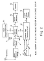
- FIG. 2 shows a simplified block diagram of an embodiment of the invention, a selective paging receiver with message display for receiving and using the paging signals of Figures 1(a) and (b).
- Electromagnetic signal waves picked up by an antenna 10 are fed to a radio receiver section 20, which recovers the baseband paging signal and sends it to a wave shape adjusting circuit 30.
- Decoder 40 can read out data from a programmable read-only memory (PROM) 50 and exchange data with a message data processing circuit 60 via a multi-line signal f.
- PROM 50 programmable read-only memory
- the output from decoder 40 is fed to a speaker 80 via an isolating buffer amplifier 70.
- Processed message data from circuit 60 is output to liquid crystal display (LCD) device 90 for displaying message information, etc. to the user.
- LCD liquid crystal display
- Operating switches SW0, SW1, SW2, SW3 enable the user to turn off an audible speaker alarm, to select operation and display modes, etc.
- Decoder 40 gets into bit synchronization using the preamble signal P, which has a repeating pattern of logical 1's and 0's, and proceeds to detection of the frame synchronizing signal SC which comes right after it.
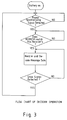
- Figure 3 is a flow chart showing the operation of the address decoder 40 in the receiver of Figure 2.
- decoder 40 reads out its prestored selective paging address from PROM 50 and starts comparing it bit by bit with received address signal A, the next item in digital signal h. If the receiver's address matches the one in the paging signal, decoder 40 activates message data processing circuit 60 by means of signal f.
- message signal M is received and its 21 information bits are error corrected by using the 10 check bits.
- decoder 40 begins watching for an end or stop signal E portion in digital signal h. When an end signal E is detected, the decoder 40 loops back to wait for detection of the next frame synchronizing signal SC.
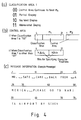
- Figures 4(a) and (b) show an example of the make-up of the Classification Area 1 and control Area appearing in the message signal of Figure 1(b).
- Classification Area 1 comprises two bits which designate the form of display that will appear in the limited display area used for messages.
- the Control Area designates the positions of the first characters of words to be displayed. Nine bits are used to designate the position of each such character. Therefore, its relative position can be as far away as the 512th position.
- Classification Area 1 of initial message portion signal M1 When the two bit Classification Area 1 of initial message portion signal M1 is "00", it indicates that the next message portion signal M1's Information Area will also be a Control Area. Then, in initial message portion signal M1 several of the bits which immediately follow Classification Area 1 are used as a further classification area, Classification Area 2, for enabling the method of display to be designated in more detail. This is explained more thoroughly below in connection with the expanded control area.
- the two bit classification Area 1 When the two bit classification Area 1 is "01", a partial display is designated.
- the next nine bits indicate the position of the first character of the first word used in the partial display, and the remaining nine bits indicate the position of the first character of the last word in the partial display.
- the Control Area might designate the string of bits "000101001000101111" .
- each group of nine bits indicates the position of the first character of a word to be extracted from the message for the key word display.
- each group of nine bits indicates the position of the first character of a word to be used in the abbreviated display, in a prestored abbreviation form if possible.
- the abbreviations that can be used in the display are prestored in PROM 50.
- next nine bits have the decimal value 54. This means that the first letter of the next word for the abbreviated display begins at position 54, at the letter "A" of "AIRPORT". Let us assume that on checking PROM 50, it is found that "AIRPORT” has a prestored abbreviation of "A. P.”. If so, in the abbreviated display "A. P.” is used in place of the word "AIRPORT".
- Classification Area 1 is "10" (Key Word Display) or "11" (Abbreviated Display), as shown at Figure 4(b) ii) only two nine bit "position-indicating" numbers can be stored in the control area. Therefore, the Key Word or Abbreviated display is limited to just two words or abbreviations, and not all the display area is used effectively.
- Classification Area 1 is instead designated as "00", as shown at Figure 4(b) i)
- the Control Area is expanded by continuing it into the 21 bit Information Area of message portion signal M2. Then, in the initial message portion signal M1 a further classification area (Classification Area 2) is provided directly behind Classification Area 1, to enable a more detailed Key Word or Abbreviated display.
- Classification Area 2 is provided directly behind Classification Area 1, to enable a more detailed Key Word or Abbreviated display.
- Classification Area 1 designates a two bit code indicating the type of summary display. However, with suitable modifications Classification Area 1 can instead designate a code, extracted from the key words of long sentences, for making certain preselected sentences.
- Classification Area 1 can designate a code which indicates how to use the key words to form such summary displays such as "NEC -- BUY", "ABC -- SELL".
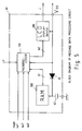
- FIG. 5 is a block diagram of the message data processing circuit 60 in the receiver of Figure 2.
- processing circuit 60 receives the user's operating instructions by reading input lines from user operating switches SW1, SW2, SW3 ( Figure 2), receives input from address decoder 40 on line f, and outputs display driving signals to the liquid crystal display (LCD) 90 ( Figure 2) on line j.
- Processing circuit 60 has a one chip CPU or microprocessor 100 that reads and writes data to a random access memory (RAM) 300 on line b1.
- An LCD driver 200 receives input about the display contents from microprocessor 100 on line b2 and outputs display driving signals on line j.
- V DD indicates a power supply voltage applied from a battery 1000 ( Figure 11) through a DC-DC converter (not shown).
- a power supply back-up capacitor 62 is provided for RAM 300.
- a diode 61 is inserted in the line from the power supply so that if voltage V DD drops below the voltage of capacitor 62, the diode will open, isolating the back-up capacitor from the power supply.
- RAM 300 acts as a first memory means for storing received message information, etc.
- the LCD driver 200 and LCD display 90 together form a display means for displaying the message information to the user.
- Microprocessor 100 acts as a display controller means for controlling the display means.
- the microprocessor responds by entering the Message Display Mode or state X2.
- the user can then choose from among a Full Message Display (X3) by SW1, a Message Number Display (X4) by SW2, and a Summary Display (X5) by SW3.
- the Message Number Display shows the number of each message so the user will know how many have been received, etc.
- the default display mode (when none of switches SW1, SW2, or SW3 is pressed after a short wait) can be a "truncated display", causing LCD display 90 to display only a preselected number of beginning characters from each of the various messages stored in RAM 300.
- microprocessor 100 causes LCD display 90, to display certain corresponding "principal items" from the messages stored in RAM 300 as a summary display in accordance with control data stored in a second memory means.
- the second memory means is discussed in more detail below.
- microprocessor 100 Furthermore, there is an easy way for the user to read out all of a message having a summary display which has caught his attention. While the summary display of that message is still being shown by LCD display 90, the user can again close switch SW0. This causes a trigger signal to be input to microprocessor 100 from decoder 40 on line f. Microprocessor 100 then returns to the Mode Selection state X1 of Figure 14. If the user next presses switch SW1 twice in succession, microprocessor 100 moves to the Message Display Mode X2 and then continues on into the Full Message Display mode X3. It reads out from RAM 300 the entire stored message information for the message, displaying it via display 90.
- microprocessor 100 The details of microprocessor 100, LCD driver 200, and RAM 300 are respectively shown in Figures 6, 7 and 8.
- microprocessor 100 has input ports 101 - 106, a port 107 for interrupts, and a serial interface 108. It also has output ports 111 - 117 and a data bus 120.
- a program memory 140 stores the sequence of program instructions that must be executed.
- a program counter 130 specifies the address of the next instruction to be read out of memory 140 and executed.
- An instruction decoder 160 decodes the program instruction information read out from program memory 140. It then provides control signals in accordance with the instructions to the various circuits for execution of the instructions.
- An arithmetic/logic unit (ALU) 150 performs arithmetic and logical operations called for by the program instructions.
- An accumulator (ACC) 170 is used in sending data to, and receiving it from, RAM 180 and the various ports 101 - 117.
- An internal RAM 180 is a scratch pad memory for storing various types of data and providing temporary storage for program status information and program counts when executing subroutines and interrupts.
- a system clock generator circuit 190 generates a series of timing pulses that determine the instruction execution cycle times.
- FIG. 7 shows a block diagram of the LCD driver 200 in the processing circuit of Figure 5, and its associated LCD display 90.
- the LCD driver 200 has a column driver 210 for controlling the columns shown by display 90, and a row driver 220 for controlling the rows.
- a display voltage controller 230 controls the voltage supplied to the LCD display, and a timing controller 240 controls timing of the driving signals to the LCD display.
- input line LCD P.S. indicates a power supply line from a battery 1000 ( Figure 11).
- a clock input line CLK supplies a system clock from system clock generator 190 on the microprocessor chip 100 ( Figure 6).
- Display driver 200 includes a data memory 250 which can store output from a character generator circuit 290 or store display data input via a serial interface 295.
- Circuit 260 is a system clock controller.
- a command decoder 270 takes in and decodes the display instructions input from microprocessor 100 via serial interface 295. It then provides control signals in accordance with the instruction contents to the various circuits for execution of the instructions.
- a data pointer 280 holds the address in data memory 250 at which it is to be written.
- data pointer 280 holds the address from which it is to be read.
- the character generating circuit 290 generates a 7 X 5 dot matrix character pattern in accordance with data input to it.
- the serial interface 295 enables display driver 200 to receive data in serial form from, and send it to, microprocessor 100.
- FIG. 8 shows a block diagram of the random access memory (RAM) 300 in the processing circuit of Figure 5.
- a serial interface 310 enables RAM 300 to receive data in serial form from, and send it to, microprocessor 100.
- An address counter 320 receives input pulses via serial interface 310.
- RAM chip 300 includes a memory array 340 having storage locations which are organized in rows and columns.
- An X-Y decoder 330 analyzes the data in the address counter 320 to designate a corresponding memory array address in memory array 340. Display data is written into, or read out of, the memory array addresses designated by X-Y decoder 330.
- a control circuit 350 receives control signals from microprocessor 100, such as those controlling the reading and writing of display data.
- Figure 9 is a block diagram of a detector circuit, for detecting frame synchronization and stop signals, used by address decoder 40 in the receiver of Figure 2.
- a 31 bit shift register 500 is provided that receives the 31 bit words of the digital paging signal h as input from wave shape adjusting circuit 30 of Figure 2.
- a clock pulse is received for timing the shifting of the data in the register.
- Logical outputs (1's and 0's) from the bits stored in the register are input to a multi-input AND gate 540, preselected input lines to AND gate 540 having inverter circuits 510, 520 and 530, as shown at register bits #1, 6, and 29.
- Figure 10 shows a simplified schematic of a detecting circuit, for detecting selective paging signals, used by the address decoder 40 in the receiver of Figure 2.
- a counter 600 receives as input a clock signal and the output of an Exclusive NOR gate 610.
- the inputs to Exclusive NOR gate 610 are the digital paging signal h from wave shape adjusting circuit 30 and a signal p from programmable ROM 50.
- the output of Exclusive NOR gate 610 will only be a logical "1" for those bits where its two inputs agree, i.e. bits of signal h that agree with the bits of signal p, prestored in PROM 50.
- Figure 11 shows a simplified schematic of an audio alarm, comprising the buffer amplifier 70 and paging speaker 80 circuits in the receiver of Figure 2.
- buffer amplifier 70 the base of an NPN transistor 730 receives, via an input resistor 710, an input alarm signal k from the output of address decoder 40 of Figure 2.
- the emitter of transistor 730 is grounded, and its collector is coupled via a resistor 720 to the base of a driving PNP transistor 740, the emitter of which is connected to battery 1000.
- the collector output of transistor 740 drives a horn or speaker alarm 800 in speaker circuit 80.
- Signal waves picked up by antenna 10 are demodulated by radio receiver section 20, and the recovered signal is shaped by wave shape adjusting circuit 30 into a serial digital paging signal h, of the type shown at Figure 1(a). This is supplied to address decoder 40. Address decoder 40 gets into bit synchronization with signal h using the preamble signal portion P shown in Figure 1(a).
- decoder 40 proceeds to a detection of the 31 bit frame synchronizing signal SC which follows the preamble signal P.
- Figure 9 shows a detector circuit used in decoder 40 to detect the frame synchronizing signal SC.
- Serial digital signal h is input into the low end of a 31 bit shift register 500 and shifted toward the right into the register, responsive to clock pulses.
- Register outputs #1 - 31, corresponding to the bits stored in register 500, are input into a multi-input AND gate 540. Certain of the register outputs are inverted before being input to gate 540, as indicated by inverter circuits 510, 520 and 530 for bits #1, 6, & 29.
- the AND gate 540 and its inputs are arranged so that when the preselected 31 bit pattern of the frame synchronizing signal SC is input to register 500, all of the inputs to AND gate 540 are logical 1's, causing it to output a 1 at gate output 541.
- Detection of synchronizing signal SC causes decoder 40 to read the next 31 bits of signal h as the address signal portion A.
- Received address signal A is compared with the receiver's prestored paging address signal by the detection circuit of Figure 10.
- the receiver's prestored digital paging address is read out from PROM 50 as signal p.
- Signal p is compared, bit by bit, with the address signal A portion of signal h by an Exclusive NOR gate 610.
- Exclusive NOR gate 610 only produces a logical 1 as an output to a counter 600 when the corresponding bits in input signals p and h match. Hence, if the received address portion A of signal h matches the receiver's prestored paging address, each of the 31 bit positions will match, and counter 600 will count up to 31.
- counter 600 is arranged to output a DET (Address Detected) signal if its count reaches 29 or more. That is, only 29 of the 31 bits of address A need to match the prestored paging address for the receiver to recognize that it is being paged.
- DET Address Detected
- a reset signal is provided on the counter 600 at a reset terminal R, to clear the counter to all 0's after the 31 bits of address A have been compared with the bits of signal h. If a DET signal is output because of a count of 29 bits or more, the DET output signal will precede the clearing of the counter by the reset signal.
- microprocessor 100 uses clock signal CL to read in a 31 bit message signal D at its input port 106 from decoder 40.
- the bits in message signal D are the 31 bits in the received message portion signal M n currently being processed.
- microprocessor 100 By means of its instruction decoder 160, microprocessor 100 translates instructions prestored in program memory 140 and processes signal D by executing them. That is, after being read in via data bus 120 and accumulator ACC 170, message signal D is written in scratchpad memory RAM 180. Unit microprocessor 100 then uses its Arithmetic Logic Unit ALU 150 to carry out the necessary computations on each of the received 31 bits of message signal D stored in scratchpad memory 180 to recover 21 error-corrected information bits from message signal D.
- Figure 12 shows an explanatory chart of the storage areas provided for storing messages and display control information.
- Figure 12 shows examples of a file area (b) and a sector area (c) in the memory which are together used to store message information.
- File names F1 - F m are assigned to correspond to a message file's position number in the file area of memory.
- the message information is stored in memory in regularly numbered memory sectors S k . Each memory sector is of fixed length (e.g. 8 characters) and usually only holds a portion of a message.
- the sector names S0 - S k are assigned to correspond to the sector's position number in the sector area of memory.
- each message file F j the names of the sectors S k which compose the message information are stored in the order needed to make up the message. For example, at (a) in Figure 12 we learn that Message M1 is stored in file F1. At file area (b) in the same figure we learn that the message is stored in sectors S0, S2, S1, S4, ... S k in that order. Using sector area (c), we can then read the message in file F1 as "MR. SATO CAME BACK FROM AMERICA ."
- the display control information is stored in memory areas indicated by (d), (e) and (f) in Figure 12.
- Area (d) is a control file area.
- control files F'1 - F' m are stored control files F'1 - F' m .
- Each control file F' j designates a summary display by means of a control code address T c followed by several character address numbers C x .
- the control code address T c in a control file F' j designates the address of a storage location in a control code area (e).
- the designated location holds the two bit display classification code from classification Areas 1 and 2 of the message portion signals.
- the two bit classification codes stored in control area (e) designate the various methods for summary displays of the received message information, such as Partial Display (01), Key Word Display (10) or Abbreviated Display (11).
- Each character address number C x in a control file F' j designates the address of a storage location in a character address area (f).
- the designated location holds the 9 bit relative position number of the first character of a word used in the summary display.
- the control files F' j have a one to one correspondence with the message files F j with the same index number j. They are arranged so the control instructions for a summary display of the message information in message file F j are in a corresponding control file number F' j . Moreover, the memory is controlled so that when the message information in a message file F j is deleted, the contents of the corresponding control file F' j are also deleted.
- the two bit display control codes are replaced by control code addresses T c .
- the two bit display control codes themselves could instead be used at the beginning of the control files F' j instead of the control code addresses T c .
- a Partial Display is a continuous string of words taken from the actual message; it is designated by indicating the first and last words in the string.
- character address C1 in character address area (f) we find the stored binary number "000 101 001", which is decimal 41. This means that the first letter of the first word of the partial display begins at character position 41, at the letter "G” of "GO".
- Memory areas (g), (h) and (i) of Figure 12 are set aside as status registers.
- Microprocessor 100 has access to both its internal scratchpad memory RAM 180 ( Figure 7) and the external RAM 300 shown in Figures 5 and 8.
- the main difference between these two RAM memories is that because scratchpad RAM 180 is on the microprocessor chip, it can be accessed faster than external RAM 300. Therefore, either of these memories could be used to provide the various message and display control memory areas shown in Figure 12.
- the memory areas for the message table (a) and the three registers at (g), (h) and (i) are provided on scratchpad memory 180.
- the three registers are respectively the F-STATUS register, the S-STATUS register, and the C-STATUS register.
- the message file area (b), sector area (c), control file area (d), control code area (e), and character address area (f) will be provided on external memory RAM 300.
- RAM 300 acts as a first memory means for storing received message information.
- RAM 180 and the "control data" storing portions of RAM 300 will together act as a second memory means for storing control data related to the display of the messages.
- the decoded message portion signals M n contain the 2-bit display control codes of Classification Areas 1 and 2 and the 9-bit character position indicating numbers of the Control Area. As these arrive, microprocessor 100 refers to the C-STATUS register to learn which character address numbers C x are not yet being used. These available address numbers C x are then stored in the control files F' j of control file area (d) to indicate the addresses where the 9-bit character position indicating numbers are stored. As each C x is used, microprocessor 100 updates the C-STATUS register by putting a "1" in the appropriate bit CSx. The addresses C x used to store the 9-bit character position indicating numbers are located in external RAM 300.
- the decoded message portion signals M n next contain the data of the message information areas. As these arrive, microprocessor 100 refers to the F-STATUS and S-STATUS registers to learn which message files F j and sectors S k are not yet being used. The available sector names are then stored in the available message files F j in the message file area (b) of external RAM 300 to indicate the sectors where a message will be stored. As each sector S k is used to store message information, microprocessor 100 updates the F-STATUS and S-STATUS registers by putting a "1" in the appropriate bits FSj and SSk.
- Microprocessor 100 transmits the 20 or 21 bits of data in each of the error corrected message portion signals M n to external RAM 300, where the data is stored for safekeeping. Using Figures 6 and 8, how this is done will now be explained. First, microprocessor 100 outputs a logical "O" at port 113 as a chip enable signal CE to put external RAM 300 in its active mode. Next, microprocessor 100 refers to the F-STATUS, S-STATUS, and C-STATUS registers in its scratchpad RAM 180 to confirm the use condition of the various memory areas in external RAM 300.
- the address information about unused memory areas is transmitted to RAM 300 by a signal SOUT via serial interface 108.
- microprocessor 100 outputs a logical "1" at port 114 to make an A/D (address/data) control signal to RAM 300 designate "address”. It also sends clock timing pulses to RAM 300 as a system clock signal SCK via interface 108.
- RAM 300 of Figure 8 interprets signal SOUT as an address signal.
- the address counter 320 and X-Y decoder 330 in RAM 300 are then used to designate the array addresses in memory array 340 at which display data is written when received.
- microprocessor 100 readies RAM 300 to receive and store output signal SOUT as message and character position data, etc. It switches the A/D signal to "0" for “data” and the R/W signal to "0" for “write”.
- Signal SOUT transmitted via serial interface 108, now carries the message and character position data, etc. to be received and stored by RAM 300.
- RAM 300 In response to the various control signals, RAM 300 writes the data received as signal SOUT in memory array 340 at the previously designated array addresses as message and character position data.
- microprocessor 100 finds that it cannot receive the message signal for two successive words, it outputs an ME (message end) signal at output port 111 to inform address decoder 40 that the message has ended. Whereupon, decoder 40 stops supplying clock signal CL to microprocessor 100 at input port 105. Or alternatively, should decoder 40 be first in detecting an end or stop signal portion E in received signal h, it automatically stops supplying clock signal CL to microprocessor 100.
- microprocessor 100 stops the processing by which it decodes the message signals. At the same time, it outputs an audio control signal AC at output port 112 to control a sound generating circuit in decoder 40.
- a sound generating signal k is applied to the base of NPN transistor 730 via input resistor 710.
- the collector output of transistor 730 is coupled to the base of PNP transistor 740 by resistor 720.
- signal k drives transistor 730 between conduction and non-conduction, the base voltage of transistor 740 is correspondingly switched between two voltage levels corresponding to logical "0" and "1".
- transistor 740 is switched between conduction and non-conduction, regulating the driving current supplied to speaker 80 by battery 1000 which is coupled to the emitter of transistor 740. This causes speaker 80 to produces an audible alarm, informing the user of the paging receiver that he has been paged.
- this type of paging receiver has an automatic alarm cutoff function (auto-reset function) which terminates the paging alarm after a preset period, such as about 8 seconds.
- auto-reset function automatic alarm cutoff function
- the pager's alarm automatically stops after a short timed interval.
- the frequency regulating crystal 41 which is coupled to decoder 40 is part of a crystal oscillator circuit within the decoder.
- the oscillator circuit produces a high frequency signal which is frequency divided to produce a periodic signal f T of about 2kHz. This is supplied to microprocessor 100 at input port 104 and used as a timing signal. The pager's alarm is terminated after a timed interval of about 8 seconds.
- the user can then select the Summary Display mode X5 by closing switch SW1 (to pass to the Message Display Mode X2) and then closing switch SW3. Closing these switches produces further trigger signals, in accordance with which the microprocessor switches into the summary display function mode of the invention.
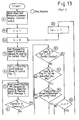
- Figure 13 shows a sample flow chart of how a summary display function can be provided by suitable programming of microprocessor 100.
- the summary display function routine begins when the microprocessor is in the Message Display Mode X2 and the user closes operating switch SW3 (Step 1). Then, an index variable i is initially set equal to the number 1 (Step 2a). This prepares microprocessor 100 to begin by processing the most recently received of the stored messages. Next a register S is initially set equal to zero (Step 2b).
- the first character address stored in control file F' j of (d) of Figure 12 is read as C x (Step 4). Then, the current character position number PN stored at character address C x is read. The microprocessor uses the position number PN to read out the character at that position in the message that is stored in RAM 300 (Step 5). This character is the first character in the first word of the summary display made from the message.
- the first character address is C1.
- the character position table at (f) of Figure 12 shows that the character position number stored at character address C1 is a binary "000 101 001", equivalent to decimal 41. Therefore, the microprocessor will read out from RAM 300 the 41st character in the message of file F1. As shown in Figure 4(c), the 41st character in this message is the "G" of "GO".
- the symbol " " is used to represent a blank character in the display.
- the microprocessor's ALU circuit 150 determines if the character which has just been read out is a blank (Step 6). If it is not, the character is loaded in a buffer register (Step 7).
- the character position number PN found at character address C x is increased by one (Step 8).
- the current character position is 41 for the letter “G”. This is increased to position 42, which corresponds to the "O" of "GO”.
- Steps 9, 10, and 11 will detect when the beginning of the last word of the Partial Display has been reached and set an indicating register S.
- the next character address in the control file F' j of (d) of Figure 12 is read as C' x (Step 9).
- the character position number stored at C' x is the position number PN of the first character in the last word of the Partial Display.
- control file F'1 begins with code address T1 for a Partial Display.
- the C' x character address is C3.
- the character position number stored at character address C3 is a binary "000 101 111", equivalent to decimal 47. Therefore, the 47th character in the message file F1 is the first character of the last word of the Partial Display. (As shown in Figure 4 (c) , this character is the "N" of "NARITA”.)
- Step 10 The current position number PN stored at character address C x is compared with the position number stored at character address C' x (Step 10). If they are equal, a register S in scratchpad RAM 180 which was initially at "0" is set to "1" for use later at Step 13 (Step 11). Otherwise, the microprocessor loops back to Step 5 to read out the next character in the message stored in RAM 300.
- the current character position number PN stored at character address C x was increased to 42 at Step 8. Since 42 does not equal the position number 47 stored at character address C3, the microprocessor loops back to Step 5 to read out the letter "O" stored at character position number 42.
- Step 6 After each additional character for the summary display is read out at Step 5, it is checked to see if it is a blank (Step 6). A blank indicates the end of the current word the characters of which are being processed.
- control code address T c in control file F' j is used to determine if the summary display is coded for a Partial Display (Step 12).
- Register S is read to see if its contents are 1 (Step 13).
- a 1 in register S means that all the characters to be used in the Partial Display have been loaded into the buffer register. Therefore, the microprocessor now sends these characters to LCD Driver 200 to have them displayed by LCD display 90 (step 20). However, a 0 in register S means that there are further words for the Partial Display not yet loaded. Therefore, there is a jump back to Step 7 to continue loading characters for the display into the buffer register.
- Step 12 the control code address T c in control file F' j is used to determine if the summary display is coded for an Abbreviated Display (Step 14). If it is, PROM 50 is chocked to see if the word just ended by the space detected at Step 6 has a prestored abbreviation message (Step 15). If it does, the abbreviation message is substituted for the word in the buffer register (step 16). Otherwise, there is no substitution, and the microprocessor moves on to Step 17.
- Step 17 the control code address T c in control file F' j indicates that the summary display is coded for a Key Word Display.
- the next character address in the control file F' j of (d) of Figure 12 is read as C' x (Step 17). If character address C' x is 0, there are no more words for the Abbreviated or Key Word Display (Step 18).
- the characters for the summary display are sent by the microprocessor for display by the display means in the same way that the full message data stored in external RAM 300 is sent and displayed.
- the flow chart of Figure 13 illustrates a technique by which various summary displays, such as Partial Displays, Key Word Displays, and Abbreviated Displays can be provided.
- a "Message Type Display” indicating the message topic or class may be needed. Or it may be desired to select key words from a message but change their order of appearance for the Key word Display, etc.
- the 00 code of Classification Area of Figure 4(a) could be used to indicate such further displays, and the number of bits in Classification Area 2 expanded to provide the necessary additional codes.
- the received paging signals have control codes preceding the message information.
- the control codes enable only the principal items which tell the gist of the messages to be selected from the message contents. These appear in a summary display that fits within the limited display area of the display panel.
- summary displays such as Partial Display, Key Word Display, Abbreviated Display, and Message Type Display, can be provided.
- Such summary displays enable the user to quickly grasp the gist of a number of relatively long received messages without having to repeatedly scroll the display to read through each message in its entirety.
Landscapes
- Physics & Mathematics (AREA)
- Electromagnetism (AREA)
- General Physics & Mathematics (AREA)
- Engineering & Computer Science (AREA)
- Computer Networks & Wireless Communication (AREA)
- Mobile Radio Communication Systems (AREA)
Claims (11)
- Récepteur sélectif de recherche de personnes avec un moyen d'affichage de messages qui est capable de recevoir des numéros de recherche de personnes sélectifs transmis et des données de messages sous forme d'un train de bits pour afficher des messages destinés à l'utilisateur, ledit récepteur comportant :- un premier moyen de mémoire (300) pour stocker des données de fragments de messages;- un moyen (100) pour identifier certains bits de commande dans ledit train de bits;- un moyen (100) pour identifier des parties particulières d'un message dans ledit train de bits en réponse auxdits certains bits de commande;- un moyen (100) pour rechercher les fragments de messages stockés pour des fragments de messages correspondant aux parties particulières de messages;- un moyen (100) pour combiner les fragments trouvés de messages correspondant aux parties particulières de messages avec les parties restantes de messages qui ne correspondent pas à l'un quelconque desdits fragments stockés de messages afin de produire un résumé du message entier dans ledit train de bits; et- un moyen de visualisation (90, 200) pour afficher ledit résumé du message entier.
- Récepteur selon la revendication 1, dans lequel ledit résumé des messages a au moins l'une des formes suivantes : la forme partielle des messages, la forme mot-clé des messages, et la forme abrégée des messages.
- Récepteur selon la revendication 1 ou 2, comprenant en outre un moyen pour dérouler des données sélectionnées parmi lesdites données de messages qui sont associées à un résumé des données de messages qui est sélectionné par un utilisateur dudit récepteur de recherche de personnes, d'où il résulte que ledit utilisateur n'a pas à lire beaucoup de données de messages qui ne présentent pas d'intérêt pour lui.
- Récepteur selon la revendication 3, dans lequel il y a une multitude desdits format des messages du résumé, un moyen répondant à l'action d'un utilisateur pour sélectionner un format parmi ladite multitude de formats, et un moyen pour afficher ledit résumé dans ledit format sélectionné par l'utilisateur.
- Récepteur selon la revendication 4, comprenant un moyen (80) pour donner à l'utilisateur un signal pour indiquer la présence d'un message.
- Procédé d'acheminement de messages à un utilisateur situé à distance d'un récepteur de recherche de personnes, ledit procédé comprenant les étapes consistant à :(a) préstocker une multitude de fragments de messages dans un récepteur de recherche de personnes;(b) transmettre des données de messages sous forme d'un train de bits audit récepteur de recherche de personnes;(c) identifier certains bits de commande dans ledit train de bits et identifier des parties particulières de messages dans ledit train de bits en réponse auxdits certains bits de commande;(d) rechercher les fragments stockés de messages en ce qui concerne des fragments de messages correspondant aux parties particulières de messages;(e) combiner les fragments trouvés de messages qui correspondent aux parties particulières de messages avec les parties restantes de messages qui ne correspondent pas à l'un quelconque desdits fragments stockés de messages afin de produire un résumé du message entier dans ledit train de bits; et(f) afficher ledit résumé du message entier.
- Procédé selon la revendication 6, comprenant une autre étape consistant à permettre à l'utilisateur de sélectionner un format pour ledit affichage desdits fragments de messages.
- Procédé selon la revendication 7, comprenant en outre l'étape consistant à permettre audit utilisateur de voir un affichage dudit message entier qui est sélectionné par ledit utilisateur, d'où il résulte qu'un utilisateur peut éliminer la nécessité de lire l'un quelconque des messages entiers à l'exception desdits résumés des messages entiers.
- Procédé selon l'une quelconque des revendications 6 à 8 comprenant en outre l'étape consistant à transmettre les données de commande ainsi que les données de messages dans ledit train de bits, et à exécuter l'étape d'identification (c) en réponse auxdites données de commande.
- Procédé selon l'une quelconque des revendications 6 à 9, comprenant en outre l'étape consistant à sélectionner l'un de nombreux formats possibles pour afficher lesdits fragments de message.
- Procédé selon l'une quelconque des revendications 6 à 10, comprenant en outre l'étape consistant à signaler audit utilisateur que ledit résumé du message entier est affiché.
Applications Claiming Priority (2)
| Application Number | Priority Date | Filing Date | Title |
|---|---|---|---|
| JP204912/85 | 1985-09-17 | ||
| JP60204912A JPH0669163B2 (ja) | 1985-09-17 | 1985-09-17 | 表示機能付無線選択呼出受信機 |
Publications (3)
| Publication Number | Publication Date |
|---|---|
| EP0218936A2 EP0218936A2 (fr) | 1987-04-22 |
| EP0218936A3 EP0218936A3 (en) | 1988-09-14 |
| EP0218936B1 true EP0218936B1 (fr) | 1993-08-04 |
Family
ID=16498437
Family Applications (1)
| Application Number | Title | Priority Date | Filing Date |
|---|---|---|---|
| EP86112784A Expired - Lifetime EP0218936B1 (fr) | 1985-09-17 | 1986-09-16 | Récepteur sélectif pour l'appel de personnes avec affichage de message |
Country Status (7)
| Country | Link |
|---|---|
| US (1) | US4766434A (fr) |
| EP (1) | EP0218936B1 (fr) |
| JP (1) | JPH0669163B2 (fr) |
| AU (1) | AU584557B2 (fr) |
| CA (1) | CA1259377A (fr) |
| DE (1) | DE3688819T2 (fr) |
| HK (1) | HK140393A (fr) |
Families Citing this family (55)
| Publication number | Priority date | Publication date | Assignee | Title |
|---|---|---|---|---|
| US4821021A (en) * | 1987-01-13 | 1989-04-11 | Nec Corporation | Selective calling radio display pager having a message recalling algorithm which simplifies operations |
| JPH0624335B2 (ja) * | 1987-02-27 | 1994-03-30 | 日本電気株式会社 | 表示付選択呼出受信機 |
| CA1317350C (fr) * | 1987-08-05 | 1993-05-04 | Michael Joseph De Luca | Recepteur de radiomessagerie a vitesse d'affichage a reglage dynamique |
| EP0308132B1 (fr) * | 1987-09-14 | 1994-06-08 | Nec Corporation | Récepteur d'appel avec une fonction d'affichage |
| JP3159121B2 (ja) * | 1987-09-30 | 2001-04-23 | カシオ計算機株式会社 | 情報受信装置 |
| DE68922337T2 (de) * | 1988-05-17 | 1995-08-31 | Casio Computer Co Ltd | Funkruf-Kommunikationssystem. |
| US5032835A (en) * | 1989-04-24 | 1991-07-16 | Motorola, Inc. | Out of range indication for radio receivers |
| US5218629A (en) * | 1989-05-12 | 1993-06-08 | Public Access Cellular Telephone, Inc. | Communication system for message display onboard mass transit vehicles |
| US5223831A (en) * | 1989-08-14 | 1993-06-29 | Motorola, Inc. | Ideographical character signalling system |
| KR960003964B1 (ko) * | 1989-08-14 | 1996-03-25 | 모토로라인코포레이티드 | 표의 문자 신호화 장치 |
| AU6638890A (en) * | 1989-11-09 | 1991-06-13 | Motorola, Inc. | Efficient message storage within a selective call receiver |
| US5258739A (en) * | 1989-11-09 | 1993-11-02 | Motorola, Inc. | Efficient message storage within a selective call receiver |
| US5146216A (en) * | 1989-12-14 | 1992-09-08 | Motorola, Inc. | Multiple message signalling protocol for a selective call receiver |
| US5283570A (en) * | 1989-12-14 | 1994-02-01 | Motorola, Inc. | Multiple format signalling protocol for a selective call receiver |
| JP2687719B2 (ja) * | 1990-11-26 | 1997-12-08 | 日本電気株式会社 | 個別選択呼出受信機 |
| US5323148A (en) * | 1991-02-28 | 1994-06-21 | Motorola, Inc. | Selective call receiver presenting the length of an alphanumeric message prior to presentation of the message |
| US5272465A (en) * | 1991-11-13 | 1993-12-21 | Telemessaging Devices, Inc. | Automatic alarm code converter |
| JPH05199163A (ja) * | 1992-01-17 | 1993-08-06 | Nec Corp | 無線選択呼出受信機 |
| WO1993022882A1 (fr) * | 1992-05-04 | 1993-11-11 | Motorola, Inc. | Recepteur et procede de presentation de type de message |
| EP0583064B1 (fr) * | 1992-07-09 | 1999-05-19 | Nec Corporation | Récepteur d'appel radio avec unité d'affichage |
| WO1994008419A1 (fr) * | 1992-09-30 | 1994-04-14 | Motorola, Inc. | Systeme de distribution de messages par courrier electronique |
| US5495234A (en) * | 1993-01-21 | 1996-02-27 | Motorola, Inc. | Method and apparatus for length dependent selective call message handling |
| EP0660281A1 (fr) * | 1993-12-24 | 1995-06-28 | Nec Corporation | Dispositif de communication radio combinable avec un modem radio pour ordinateur |
| US6427064B1 (en) | 1994-01-05 | 2002-07-30 | Daniel A. Henderson | Method and apparatus for maintaining a database in a portable communication device |
| US6278862B1 (en) | 1994-01-05 | 2001-08-21 | Daniel A. Henderson | Method and apparatus for enhancing the efficient communication of information in an alphanumeric paging network |
| US7426264B1 (en) | 1994-01-05 | 2008-09-16 | Henderson Daniel A | Method and apparatus for improved personal communication devices and systems |
| US7266186B1 (en) | 1994-01-05 | 2007-09-04 | Intellect Wireless Inc. | Method and apparatus for improved paging receiver and system |
| US5539529A (en) * | 1994-04-04 | 1996-07-23 | Merchant; Zaffer S. | Facsimile communication with selective call receivers |
| JP3671468B2 (ja) * | 1994-11-11 | 2005-07-13 | カシオ計算機株式会社 | 受信装置及び表示制御方法 |
| JP3012487B2 (ja) * | 1995-06-06 | 2000-02-21 | 日本電気株式会社 | 伝言表示機能付き無線選択呼出受信機 |
| KR0165210B1 (ko) * | 1995-06-26 | 1999-02-01 | 김광호 | 무선호출수신기의 음성호출장치 및 방법 |
| JP2957445B2 (ja) * | 1995-08-21 | 1999-10-04 | 静岡日本電気株式会社 | 無線選択呼出受信機 |
| JP2702463B2 (ja) * | 1995-11-13 | 1998-01-21 | 静岡日本電気株式会社 | 無線選択呼出受信機 |
| JP3497028B2 (ja) * | 1995-11-17 | 2004-02-16 | 松下電器産業株式会社 | メッセージ通知システム、メッセージ通知方法およびメッセージ受信端末 |
| DE19610493C2 (de) * | 1996-03-18 | 1998-07-30 | Deutsche Telekom Mobil | Verfahren zur Verbreitung von Mehrwertinformationen |
| JPH09322218A (ja) * | 1996-03-29 | 1997-12-12 | Casio Comput Co Ltd | 送受信システムもしくはそれに用いられる装置と方法 |
| JPH09331302A (ja) * | 1996-04-12 | 1997-12-22 | Casio Comput Co Ltd | 送受信システムもしくはそれに用いられる装置及び方法 |
| JP2919354B2 (ja) * | 1996-05-28 | 1999-07-12 | 静岡日本電気株式会社 | 個別選択呼出受信機 |
| JP2919393B2 (ja) * | 1996-10-29 | 1999-07-12 | 静岡日本電気株式会社 | パスワードによる呼出制御装置および呼出制御方法 |
| JP2923868B2 (ja) * | 1996-11-05 | 1999-07-26 | 日本電気株式会社 | 無線装置 |
| JP2972632B2 (ja) * | 1997-03-26 | 1999-11-08 | 静岡日本電気株式会社 | 無線選択呼出受信機 |
| JP3071716B2 (ja) * | 1997-04-24 | 2000-07-31 | 静岡日本電気株式会社 | 情報受信装置 |
| US5936547A (en) * | 1997-07-15 | 1999-08-10 | Ameritech Corporation | System and method for providing user-selected information to a paging-capable device |
| US6233430B1 (en) * | 1997-09-19 | 2001-05-15 | Richard J. Helferich | Paging transceivers and methods for selectively retrieving messages |
| US6060997A (en) * | 1997-10-27 | 2000-05-09 | Motorola, Inc. | Selective call device and method for providing a stream of information |
| JPH11266472A (ja) * | 1998-03-18 | 1999-09-28 | Nec Shizuoka Ltd | 表示機能付き無線選択呼出受信機 |
| JP3226164B2 (ja) * | 1998-11-06 | 2001-11-05 | 日本電気株式会社 | 移動携帯情報端末装置およびそのデータ表示方法 |
| US6260060B1 (en) * | 1998-11-13 | 2001-07-10 | Motorola Inc. | Method and apparatus for enhancing a message preview mode in a messaging unit |
| DE19861323B4 (de) | 1998-12-08 | 2006-02-16 | Robert Bosch Gmbh | Verfahren zur Übertragung von Kurznachrichten |
| CN1136666C (zh) | 1999-05-13 | 2004-01-28 | 松下电器产业株式会社 | 移动体通信终端装置 |
| JP2001028788A (ja) * | 1999-05-13 | 2001-01-30 | Matsushita Electric Ind Co Ltd | 移動体通信端末装置 |
| US6993049B2 (en) * | 2000-06-26 | 2006-01-31 | Koninklijke Philips Electronics N.V. | Communication system |
| JP2003269969A (ja) | 2002-03-13 | 2003-09-25 | Sony Corp | ナビゲーション装置、地点情報の表示方法およびプログラム |
| JP5219664B2 (ja) * | 2008-07-14 | 2013-06-26 | キヤノン株式会社 | 表示装置及び画像形成装置、並びに表示方法及びプログラム |
| US8594160B2 (en) * | 2009-04-02 | 2013-11-26 | Panasonic Corporation | Radio transmitting/receiving circuit, wireless communication apparatus, and radio transmitting/receiving method |
Family Cites Families (12)
| Publication number | Priority date | Publication date | Assignee | Title |
|---|---|---|---|---|
| US3757037A (en) * | 1972-02-02 | 1973-09-04 | N Bialek | Video image retrieval catalog system |
| US3976995A (en) * | 1975-05-22 | 1976-08-24 | Sanders Associates, Inc. | Precessing display pager |
| US4336524A (en) * | 1979-07-17 | 1982-06-22 | Levine Alfred B | Video display pager receiver with memory |
| JPS5665537A (en) * | 1979-11-01 | 1981-06-03 | Nec Corp | Individual selection callout receiver with display |
| JPS58500339A (ja) * | 1981-02-26 | 1983-03-03 | ゼネラル・エレクトリック・カンパニイ | 多重フォ−マット・デ−タ・ディスプレィ装置 |
| US4385295A (en) * | 1981-09-29 | 1983-05-24 | Motorola, Inc. | Pager with visible display indicating unread messages |
| DE3209187C2 (de) * | 1982-03-13 | 1985-01-10 | Triumph-Adler Aktiengesellschaft für Büro- und Informationstechnik, 8500 Nürnberg | Verfahren zur Darstellung eines Textes auf einer einzeiligen Anzeigevorrichtung eines Texterstellungsgerätes |
| JPS58178642A (ja) * | 1982-04-13 | 1983-10-19 | Nec Corp | 表示付き個別選択呼出受信機 |
| JPS58209238A (ja) * | 1982-05-31 | 1983-12-06 | Nec Corp | メツセ−ジ情報の受信機能を備えた無線個別選択呼出受信機 |
| GB2124419B (en) * | 1982-05-31 | 1985-09-18 | Nec Corp | Radio paging apparatus |
| JPS5939130A (ja) * | 1982-08-27 | 1984-03-03 | Nec Corp | 表示機能付無線選択呼出受信機 |
| EP0136677B1 (fr) * | 1983-09-30 | 1990-08-16 | Nec Corporation | Récepteur d'appel multifonctions susceptible de réduire le nombre de touches |
-
1985
- 1985-09-17 JP JP60204912A patent/JPH0669163B2/ja not_active Expired - Fee Related
-
1986
- 1986-09-11 US US06/906,148 patent/US4766434A/en not_active Expired - Lifetime
- 1986-09-16 EP EP86112784A patent/EP0218936B1/fr not_active Expired - Lifetime
- 1986-09-16 CA CA000518236A patent/CA1259377A/fr not_active Expired
- 1986-09-16 DE DE86112784T patent/DE3688819T2/de not_active Expired - Fee Related
- 1986-09-17 AU AU62766/86A patent/AU584557B2/en not_active Ceased
-
1993
- 1993-12-23 HK HK1403/93A patent/HK140393A/en not_active IP Right Cessation
Also Published As
| Publication number | Publication date |
|---|---|
| AU584557B2 (en) | 1989-05-25 |
| US4766434A (en) | 1988-08-23 |
| DE3688819T2 (de) | 1994-03-17 |
| CA1259377A (fr) | 1989-09-12 |
| EP0218936A2 (fr) | 1987-04-22 |
| HK140393A (en) | 1993-12-31 |
| JPS6265528A (ja) | 1987-03-24 |
| EP0218936A3 (en) | 1988-09-14 |
| DE3688819D1 (de) | 1993-09-09 |
| JPH0669163B2 (ja) | 1994-08-31 |
| AU6276686A (en) | 1987-03-19 |
Similar Documents
| Publication | Publication Date | Title |
|---|---|---|
| US4766434A (en) | Selective paging receiver with message display | |
| US4646081A (en) | Radio paging receiver operable on a word scrolling basis | |
| US6658409B1 (en) | Message data reception device and method for controlling display of message data items and other data items related to the message | |
| US4768031A (en) | Radio paging receiver having a message protection capability | |
| KR970068196A (ko) | 데이터통신시스템 및 해당 시스템에 적용되는 통신기능을 구비한 정보관리장치 | |
| EP0275165B1 (fr) | Dispositif d'affichage d'appel sélectif radio | |
| US5396229A (en) | Selective calling receiver | |
| KR950006700B1 (ko) | 메모리 백업이 정확한지의 여부를 알릴 수 있는 무선 페이저 수신기 | |
| KR910002766B1 (ko) | 메모리백업의 정확성 여부를 용이하게 점검할 수 있는 무선호출수신기 | |
| KR970000564B1 (ko) | 선정된 메시지를 디스플레이 할 수 있는 무선 페이징 수신기 | |
| US4857911A (en) | Multifunctional pager receiver capable of reducing the member of manual switches | |
| US5764157A (en) | Radio paging receiver with display unit having update means to eliminate redundant messages | |
| JPH0750951B2 (ja) | ページングシステム | |
| JPS6074736A (ja) | 表示機能付無線選択呼出受信機 | |
| US5453739A (en) | Radio paging receiver capable of displaying messages as desired | |
| US5844499A (en) | Method and apparatus for recovering erased calling messages in radio pager | |
| US5329538A (en) | Circuit for providing digital data having high clarity in a digital signal receiver | |
| US5973615A (en) | Display pager having message finder responsive to user-entered time indication | |
| US6429772B1 (en) | Pager with unread pager message indicator | |
| JP2893079B2 (ja) | メッセージ受信機 | |
| JPH0445316Y2 (fr) | ||
| JPH0474901B2 (fr) | ||
| JPH03766Y2 (fr) | ||
| JPH0242256B2 (fr) | ||
| GB2267987A (en) | Alphabetic display |
Legal Events
| Date | Code | Title | Description |
|---|---|---|---|
| PUAI | Public reference made under article 153(3) epc to a published international application that has entered the european phase |
Free format text: ORIGINAL CODE: 0009012 |
|
| 17P | Request for examination filed |
Effective date: 19860916 |
|
| AK | Designated contracting states |
Kind code of ref document: A2 Designated state(s): DE GB SE |
|
| PUAL | Search report despatched |
Free format text: ORIGINAL CODE: 0009013 |
|
| AK | Designated contracting states |
Kind code of ref document: A3 Designated state(s): DE GB SE |
|
| 17Q | First examination report despatched |
Effective date: 19910416 |
|
| GRAA | (expected) grant |
Free format text: ORIGINAL CODE: 0009210 |
|
| AK | Designated contracting states |
Kind code of ref document: B1 Designated state(s): DE GB SE |
|
| PG25 | Lapsed in a contracting state [announced via postgrant information from national office to epo] |
Ref country code: SE Effective date: 19930804 |
|
| REF | Corresponds to: |
Ref document number: 3688819 Country of ref document: DE Date of ref document: 19930909 |
|
| PLBE | No opposition filed within time limit |
Free format text: ORIGINAL CODE: 0009261 |
|
| STAA | Information on the status of an ep patent application or granted ep patent |
Free format text: STATUS: NO OPPOSITION FILED WITHIN TIME LIMIT |
|
| 26N | No opposition filed | ||
| REG | Reference to a national code |
Ref country code: GB Ref legal event code: IF02 |
|
| PGFP | Annual fee paid to national office [announced via postgrant information from national office to epo] |
Ref country code: GB Payment date: 20030910 Year of fee payment: 18 |
|
| PGFP | Annual fee paid to national office [announced via postgrant information from national office to epo] |
Ref country code: DE Payment date: 20030925 Year of fee payment: 18 |
|
| PG25 | Lapsed in a contracting state [announced via postgrant information from national office to epo] |
Ref country code: GB Free format text: LAPSE BECAUSE OF NON-PAYMENT OF DUE FEES Effective date: 20040916 |
|
| PG25 | Lapsed in a contracting state [announced via postgrant information from national office to epo] |
Ref country code: DE Free format text: LAPSE BECAUSE OF NON-PAYMENT OF DUE FEES Effective date: 20050401 |
|
| GBPC | Gb: european patent ceased through non-payment of renewal fee |
Effective date: 20040916 |