EP0218938B1 - Matériaux et dispositifs optiquement non linéaires - Google Patents
Matériaux et dispositifs optiquement non linéaires Download PDFInfo
- Publication number
- EP0218938B1 EP0218938B1 EP19860112794 EP86112794A EP0218938B1 EP 0218938 B1 EP0218938 B1 EP 0218938B1 EP 19860112794 EP19860112794 EP 19860112794 EP 86112794 A EP86112794 A EP 86112794A EP 0218938 B1 EP0218938 B1 EP 0218938B1
- Authority
- EP
- European Patent Office
- Prior art keywords
- film
- optical element
- optical
- recited
- waveguide
- Prior art date
- Legal status (The legal status is an assumption and is not a legal conclusion. Google has not performed a legal analysis and makes no representation as to the accuracy of the status listed.)
- Expired - Lifetime
Links
Images

Classifications
-
- G—PHYSICS
- G02—OPTICS
- G02F—OPTICAL DEVICES OR ARRANGEMENTS FOR THE CONTROL OF LIGHT BY MODIFICATION OF THE OPTICAL PROPERTIES OF THE MEDIA OF THE ELEMENTS INVOLVED THEREIN; NON-LINEAR OPTICS; FREQUENCY-CHANGING OF LIGHT; OPTICAL LOGIC ELEMENTS; OPTICAL ANALOGUE/DIGITAL CONVERTERS
- G02F1/00—Devices or arrangements for the control of the intensity, colour, phase, polarisation or direction of light arriving from an independent light source, e.g. switching, gating or modulating; Non-linear optics
- G02F1/35—Non-linear optics
- G02F1/355—Non-linear optics characterised by the materials used
- G02F1/361—Organic materials
- G02F1/3615—Organic materials containing polymers
- G02F1/3617—Organic materials containing polymers having the non-linear optical group in a side chain
-
- G—PHYSICS
- G02—OPTICS
- G02F—OPTICAL DEVICES OR ARRANGEMENTS FOR THE CONTROL OF LIGHT BY MODIFICATION OF THE OPTICAL PROPERTIES OF THE MEDIA OF THE ELEMENTS INVOLVED THEREIN; NON-LINEAR OPTICS; FREQUENCY-CHANGING OF LIGHT; OPTICAL LOGIC ELEMENTS; OPTICAL ANALOGUE/DIGITAL CONVERTERS
- G02F1/00—Devices or arrangements for the control of the intensity, colour, phase, polarisation or direction of light arriving from an independent light source, e.g. switching, gating or modulating; Non-linear optics
- G02F1/01—Devices or arrangements for the control of the intensity, colour, phase, polarisation or direction of light arriving from an independent light source, e.g. switching, gating or modulating; Non-linear optics for the control of the intensity, phase, polarisation or colour
- G02F1/061—Devices or arrangements for the control of the intensity, colour, phase, polarisation or direction of light arriving from an independent light source, e.g. switching, gating or modulating; Non-linear optics for the control of the intensity, phase, polarisation or colour based on electro-optical organic material
- G02F1/065—Devices or arrangements for the control of the intensity, colour, phase, polarisation or direction of light arriving from an independent light source, e.g. switching, gating or modulating; Non-linear optics for the control of the intensity, phase, polarisation or colour based on electro-optical organic material in an optical waveguide structure
-
- G—PHYSICS
- G02—OPTICS
- G02F—OPTICAL DEVICES OR ARRANGEMENTS FOR THE CONTROL OF LIGHT BY MODIFICATION OF THE OPTICAL PROPERTIES OF THE MEDIA OF THE ELEMENTS INVOLVED THEREIN; NON-LINEAR OPTICS; FREQUENCY-CHANGING OF LIGHT; OPTICAL LOGIC ELEMENTS; OPTICAL ANALOGUE/DIGITAL CONVERTERS
- G02F1/00—Devices or arrangements for the control of the intensity, colour, phase, polarisation or direction of light arriving from an independent light source, e.g. switching, gating or modulating; Non-linear optics
- G02F1/35—Non-linear optics
- G02F1/355—Non-linear optics characterised by the materials used
- G02F1/361—Organic materials
- G02F1/3615—Organic materials containing polymers
-
- H—ELECTRICITY
- H01—ELECTRIC ELEMENTS
- H01S—DEVICES USING THE PROCESS OF LIGHT AMPLIFICATION BY STIMULATED EMISSION OF RADIATION [LASER] TO AMPLIFY OR GENERATE LIGHT; DEVICES USING STIMULATED EMISSION OF ELECTROMAGNETIC RADIATION IN WAVE RANGES OTHER THAN OPTICAL
- H01S3/00—Lasers, i.e. devices using stimulated emission of electromagnetic radiation in the infrared, visible or ultraviolet wave range
- H01S3/10—Controlling the intensity, frequency, phase, polarisation or direction of the emitted radiation, e.g. switching, gating, modulating or demodulating
- H01S3/106—Controlling the intensity, frequency, phase, polarisation or direction of the emitted radiation, e.g. switching, gating, modulating or demodulating by controlling devices placed within the cavity
- H01S3/107—Controlling the intensity, frequency, phase, polarisation or direction of the emitted radiation, e.g. switching, gating, modulating or demodulating by controlling devices placed within the cavity using electro-optic devices, e.g. exhibiting Pockels or Kerr effect
-
- G—PHYSICS
- G02—OPTICS
- G02F—OPTICAL DEVICES OR ARRANGEMENTS FOR THE CONTROL OF LIGHT BY MODIFICATION OF THE OPTICAL PROPERTIES OF THE MEDIA OF THE ELEMENTS INVOLVED THEREIN; NON-LINEAR OPTICS; FREQUENCY-CHANGING OF LIGHT; OPTICAL LOGIC ELEMENTS; OPTICAL ANALOGUE/DIGITAL CONVERTERS
- G02F1/00—Devices or arrangements for the control of the intensity, colour, phase, polarisation or direction of light arriving from an independent light source, e.g. switching, gating or modulating; Non-linear optics
- G02F1/01—Devices or arrangements for the control of the intensity, colour, phase, polarisation or direction of light arriving from an independent light source, e.g. switching, gating or modulating; Non-linear optics for the control of the intensity, phase, polarisation or colour
- G02F1/21—Devices or arrangements for the control of the intensity, colour, phase, polarisation or direction of light arriving from an independent light source, e.g. switching, gating or modulating; Non-linear optics for the control of the intensity, phase, polarisation or colour by interference
- G02F1/225—Devices or arrangements for the control of the intensity, colour, phase, polarisation or direction of light arriving from an independent light source, e.g. switching, gating or modulating; Non-linear optics for the control of the intensity, phase, polarisation or colour by interference in an optical waveguide structure
-
- G—PHYSICS
- G02—OPTICS
- G02F—OPTICAL DEVICES OR ARRANGEMENTS FOR THE CONTROL OF LIGHT BY MODIFICATION OF THE OPTICAL PROPERTIES OF THE MEDIA OF THE ELEMENTS INVOLVED THEREIN; NON-LINEAR OPTICS; FREQUENCY-CHANGING OF LIGHT; OPTICAL LOGIC ELEMENTS; OPTICAL ANALOGUE/DIGITAL CONVERTERS
- G02F1/00—Devices or arrangements for the control of the intensity, colour, phase, polarisation or direction of light arriving from an independent light source, e.g. switching, gating or modulating; Non-linear optics
- G02F1/29—Devices or arrangements for the control of the intensity, colour, phase, polarisation or direction of light arriving from an independent light source, e.g. switching, gating or modulating; Non-linear optics for the control of the position or the direction of light beams, i.e. deflection
- G02F1/31—Digital deflection, i.e. optical switching
- G02F1/313—Digital deflection, i.e. optical switching in an optical waveguide structure
- G02F1/3132—Digital deflection, i.e. optical switching in an optical waveguide structure of directional coupler type
-
- G—PHYSICS
- G02—OPTICS
- G02F—OPTICAL DEVICES OR ARRANGEMENTS FOR THE CONTROL OF LIGHT BY MODIFICATION OF THE OPTICAL PROPERTIES OF THE MEDIA OF THE ELEMENTS INVOLVED THEREIN; NON-LINEAR OPTICS; FREQUENCY-CHANGING OF LIGHT; OPTICAL LOGIC ELEMENTS; OPTICAL ANALOGUE/DIGITAL CONVERTERS
- G02F1/00—Devices or arrangements for the control of the intensity, colour, phase, polarisation or direction of light arriving from an independent light source, e.g. switching, gating or modulating; Non-linear optics
- G02F1/35—Non-linear optics
- G02F1/37—Non-linear optics for second-harmonic generation
Definitions
- This invention relates to nonlinear optical elements comprising the features of the preamble of claim 1 and to nonlinear optical devices such as electrooptic modulators and switches, frequency converters and data processors and optically nonlinear materials useful in such devices.
- Electrooptical modulators, switches and optical parametric devices based upon the nonlinear optical properties of materials are known in the art. Generally, these devices have utilized inorganic crystals, e.g., LiNbO3 as the optically nonlinear media. More recently, organic crystalline materials, e.g., 2-methyl-4-nitroanaline, have been shown to have a figure of merit as an optically nonlinear active material which is greater than that of LiNbO3. In addition, due to the electronic states associated with the effect, the organic crystalline materials not only have large intrinsic second order nonlinear optical susceptabilities, but potentially possess very fast switching times. Further, associated with such second order nonlinear optical effect is a linear electrooptical effect.
- inorganic crystals e.g., LiNbO3
- organic crystalline materials e.g., 2-methyl-4-nitroanaline
- the organic crystalline materials due to the electronic states associated with the effect, the organic crystalline materials not only have large intrinsic second order nonlinear optical susceptabilities,
- glassy in connection with polymer is meant in its commonly understood and generally used sense to designate an amorphous structure without long range three-dimensional order.
- a nonlinear optical element comprises an optically clear polymer host and organic dopant molecules having a nonzero second order optical susceptibility, being incorporated and directionally aligned in said polymer host; and said polymer host is a glassy polymer.
- an optical device comprises the aforementioned nonlinear optical element and means for providing an optical input to and an output from said element.
- said device When said device is employed in an electrooptic mode it includes means for applying an electric field and/or optical input to said element for altering an optical property thereof.
- any optically nonlinear device is the nonlinear optical medium employed therein.
- a noncrystalline medium comprising a non-centrosymmetric organic molecule having a non-zero second order optical susceptability incorporated in an optically clear glassy polymer in an ordered or directionally aligned arrangement of the organic molecules.
- Such second order nonlinear optical media can be prepared directly on a desired substrate or can be made as a free film or tape. It may be noted that this optically nonlinear media can be utilized as an optical waveguide as well as in electrooptic devices.
- electrooptic devices here is electrical control of the direction, phase, frequency and/or amplitude of lightwave signals.
- optical parametric devices there is mixing of two optical input signals to generate two optical output signals whose frequencies are the sum and difference of the two input frequencies and whose amplitudes are related to the input amplitudes.
- one input beam is converted to one output beam whose frequency is twice that of the input beam.
- novel devices can be integrated with electronic devices on a semiconductor chip or laser or other solid state device to form a monolithic optical or electrooptical semiconductor device. Examples of such devices are described below.
- the coupler 1 comprises a substrate 2, e.g., glass, quartz or Si, a pair of spaced channel waveguides 3 and 4 on one surface of the substrate 2 and a pair of electrodes 5 and 6, one electrode associated with and contiguous to each channel waveguides 3 and 4, respectively.
- the electrodes 5 and 6 are positioned adjacent to the waveguide in this narrowly spaced region so as to maximize the electric field developed across the waveguides upon application of a voltage of the electrodes.
- the electrodes 5 and 6 may employ a single top electrode over the waveguides and a bottom electrode below the waveguides to enhance the field for a given applied voltage.
- the device may contain a protective polymer overcoat 7, e.g., a clear epoxy or acrylate polymer, to protect the waveguides 3 and 4.
- the electrooptic waveguides 3 and 4 which are about 2 ⁇ m thick are comprised of an optical quality glassy polymer host having doped therein a directionally ordered array of non-centrosymmetric organic molecules which exhibit second order optical susceptability in response to an applied field.
- light preferably from a monochromatic single mode source, e.g., a laser
- a monochromatic single mode source e.g., a laser
- the electromagnetic field extends beyond the confines of the waveguide 3 a distance which is greater than the gap distance between the parallel portions of the upper and lower waveguides and penetrates the lower waveguide 4 and is propagated therethrough as well. If the length of the parallel portions of the waveguide are selected such that an antinode exists at the point of the lower waveguide 4 where the waveguides 3 and 4 start to deviate, the light (electromagnetic waves) will essentially be emitted from the lower waveguides at S2. This is the crossover or switched configuration.
- the electrooptical effect produced thereby causes the light to be transmitted directly in the upper waveguide and exit as shown by S3.
- the voltage causing the maximum straight-through transmission is given by where U is the applied voltage, ⁇ is the wavelength, n the index of refraction of the waveguide, r the electrooptic coefficient of the waveguide, d the waveguide separation distance, L the length of the narrowly spaced parallel portions, and ⁇ the overlap integral between applied electric field and the optical field in the waveguide.
- FIG. 2 shows an integrated laser tuner and frequency stabilizer using the electrooptic medium described herein.
- a junction or injection laser 20 is grown on a semiconductor substrate 21, e.g., a GaAs laser on a GaAs substrate.
- a 1-3 ⁇ m thick electrooptic film 22 lies adjacent and contiguous with the laser junction 23 to provide a waveguide for the light emitted at the junction 23.
- the film 22 is provided with opposing electrodes 24 and 25, on one surface thereof, as shown, or on opposite surfaces, i.e., one electrode 24a between the film and the substrate and one electrode 25a on the top surface of the film so as to provide means for applying an electric field within the electrooptical film 22.
- electrode 25a can be a highly doped portion of the substrate 21.
- the electrooptic effect of the film under an applied field results in a tunable filter or frequency stabilizer for the laser output.
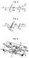
- FIG. 3 shows the optically onlinear medium used in an optical parametric device for second harmonic frequency generation.
- an incident light beam 30 at frequency ⁇ impinges upon the optically nonlinear film 31. Due to the nonlinear optical properties of the film 31, two colinear beams 32 and 33 are emitted, one at the same frequency, ⁇ , and one at twice the frequency, 2 ⁇ .
- the emerging colinear beams 32 and 33 are passed through a prism 34 to spatially separate the two wavelengths 32 and 33.
- the beam 32 at 2 ⁇ is now available to be used.
- FIG. 4 shows the use of the electrooptic film in an electrooptic phase/intensity modulator.
- incident light 40 having a polarization P1 is passed through the electrooptic film 41 which is provided with transparent electrodes 42 and 43 on opposing surfaces of the film 41.
- the natural bi-refringence of the film causes a change of polarization of the light to P2.
- a voltage is applied to the film by means of a voltage source 44 applied across the electrodes 42 and 43, an electric field is generated within the film 41.
- the electric field causes a change in the film's index of refraction, thereby altering the bi-refringence.
- a polarization modulation between the values P2 and P3 can be achieved by the periodic applications and/or removal of the voltage to the film 41.
- An intensity modulation can be achieved by placing a polarizer 45 at the output beam which is oriented to allow the passage of either P2 or P3, but not both.
- the nonlinear optical film of the devices of FIGS. 4 and 5, in practice, are preferably deposited on a substrate.
- FIG. 5 shows a guided wave electrooptic intensity modulator employing an electrooptic material as described herein.
- a film 50 of the electrooptic material is formed on a conductive substrate 51 having an insulative coating 52.
- the film 50 has a Mach-Zehnder two-arm interferrometric waveguide structure.
- a top electrode 53 is placed on one arm 54 of the interferromitric waveguide structure.
- the substrate is kept at ground potential.
- As voltage is applied to and removed from across the arm 54 by means of top electrode 53 and conducting substrate 51, an electric field is produced in the arm 54 of the interferrometer. This field changes the index of refration of the material due to the linear electrooptic effect possessed by the film 50.
- the second order nonlinear optical medium useful for the above mentioned and other electrooptic and optical parametric devices comprises an optically clear glassy polymer having a no-centrosymmetric organic molecule which exhibits a non-zero second order optical susceptability in a ordered (directionally aligned) arrangement within said polymer. Since the magnitude of the effect is a linear function of the concentration of the organic molecule in the polymer, it is advantageous to utilize a system where the organic molecule is highly soluble within the glassy polymer host.
- polymers may be suitable hosts, e.g., polymers of acrylates, methacrylates, clear epoxies, styrene and polycarbonate, we have found thus far that polymethylmethacrylate is generally preferred as the polymeric host material for the classes of nonlinear organic molecules investigated.
- R1 is a strong electron withdraing group as known in the art, e.g., NO2, and SO2
- R and R2 is an electron donating or netural group, e.g., where R x and/or R y are H or an alkyl group or derivative thereof such as -C2H5, -C2H4OH, C3H7, etc.
- R x and/or R y are H or an alkyl group or derivative thereof such as -C2H5, -C2H4OH, C3H7, etc.
- R x and/or R y are H or an alkyl group or derivative thereof such as -C2H5, -C2H4OH, C3H7, etc.
- R x and/or R y are H or an alkyl group or derivative thereof such as -C2H5, -C2H4OH, C3H7, etc.
- R x and/or R y are H or an alkyl group or derivative thereof such as
- the maximum amount of active nonlinear optic compound as can be dissolved in the glassy polymer matrix in order to maximize the bulk second order nonlinear optical effect.
- the particular polymer most suitable with any specific nonlinear optical compound may depend upon the solubility of the compound in the polymer which can easily be determined.
- a particularly suitable system appears to be the azo dye, disperse red 1 (R1 is NO2 and R2 is dissolved in polymethylmethacrylate (PMMA) to a concentration of up to 18 weight percent.
- PMMA polymethylmethacrylate
- Other compounds which are expected to give similar results in PMMA or other acrylate based polymers, e.g., polyethylacrylate, polymethylacrylate and polyethylmethacrylate are those where R1 is -NO2 and R2 is either NH2 or NR 3 2 where R3 are alkyl groups such as CH3 , C2H5, C3H7 or the like or one such alkyl group and a hydrogen atom.
- the azo dyes such as disperse orange 3 have also been found to be suitable in an epoxy host.
- the active non-centrosymmetric organic material must be directionally oriented in the polymer matrix. This orientation is accomplished by poling the molecules in the polymer under the influence of an electric field under conditions where the polymer is fluid (e.g., above its glass transistion temperature or mixed with a solvent therefor). The field is retained until the polymer film hardens by reducing the temperature or evaporating the solvent. Upon hardening, the oriented active molecules remain in their ordered position in the polymer. Unoriented films do not exhibit the second order nonlinear optical properties of the oriented films due to the cancellation of the microscopic molecular effects on a macroscopic level caused by random orientation of the molecules. It should also be possible to achieve an ordered film under an electric field applied across the active molecule dissolved in a liquid monomer which is spread on a substrate to form a film and polymerized in situ.
- An example of the preparation of a suitable nonlinear optical film is as follows.
- the polymer e.g., PMMA
- a suitable solvent e.g., DMSO, methylene chloride, chlorobenzene, acetone, ethyl or methyl cellosolve and cellosolve acetate.
- the optically nonlinear material is dissolved in the polymer-solvent solution.
- the concentration of the dye in the polymer is preferably about 18%.
- the substrate upon which the optically nonlinear film is to be prepared is thoroughly cleaned, preferably in a dust free atmosphere.
- Typical substrates are glass, quartz, aluminum, silicon wafer, thermal oxide coated silicon wafers and conductive indium-tin oxide-coated glass.
- a suitable substrate cleaning procedure employs an immersion in a heated solution comprising H2O, NH4OH and H2O2 in a volume ratio of 10:2.5:2 followed by a rinse with conductivity grade water and drying in an inert atmosphere.
- the substrate is then coated with the solution of the nonlinear optical material in the polymer such as by means of spin coating a 1 ⁇ m thick film on the substrate and removing the solvent by baking.
- Thicker films e.g., up to 5 ⁇ m are preferably prepared by multiple coatings followed by baking after each coating.
- multiple coatings of about 25 ⁇ m per coating may be achieved by spray coating or doctor blading. It may be noted that by techniques well known in the art, high quality photoresist patterns can be applied to unmetallized films to form films having feature sizes of for example 4-50 ⁇ m, which may be useful in some of the novel devices previously described.
- the substrate In order to pole or orient the active optically nonlinear molecules in the deposited film, it is preferred that the substrate have provided a conductor on the surface on which the optically nonlinear film or a buffer layer beneath the film is to be deposited.
- This can be a transparent tin oxide, indium oxide or indium tin-oxide conductor or a transparent or non-transparent metallic conductor deposited for example by sputtering.
- a top conductor is formed over the deposited film such as by sputtering a thin (100-1000 A.) gold layer on the deposited film.
- the film sandwiched between electrodes is then raised about 5°C-40°C above the glass-rubber transition temperature of the polymer by slow heating.
- the preferred azo dye in PMMA is heated at a rate of 5-15°C/minute to a temperature of from 115°-130°C.
- a poling voltage which aligns the optically nonlinear molecules in the polymer is applied across the film and maintained for from 1-10 minutes. The voltage applied depends upon the film thickness. A voltage which creates a field of at least about 1x10⁵V/cm is desirable.
- the film is slowly cooled at a rate of about 10°C/minute and annealed for 5-15 minutes at a temperature just below the glass transition temperature ( 90°C for the azo dye in PMMA). After annealing it is slowly cooled to room temperature at about 15°C/minute and the poling voltage is removed.
- the slow heating, cooling, and annealing is to prevent defects from arising, minimizing or eliminating strain and minimizing free volume in the film.
- the top electrode layer may then be removed by abrasion or other means or it may be left on. Also the film may be patterned as previously mentioned by standard photoresist - etch techniques.
- the film is typically applied to a transparent indium tin oxide conductor on a glass substrate and the top electrode is a transparent sputtered gold electrode.
- the film is typically deposited on a thermal oxide coated silicon wafer and its top surface is metallized by sputtering 2000-3000A. of Al on the film.
Landscapes
- Physics & Mathematics (AREA)
- Nonlinear Science (AREA)
- Optics & Photonics (AREA)
- General Physics & Mathematics (AREA)
- Electromagnetism (AREA)
- Engineering & Computer Science (AREA)
- Plasma & Fusion (AREA)
- Optical Integrated Circuits (AREA)
Claims (22)
- Un élément optique non linéaire comprenant :- un polymère hôte transparent au point de vue optique; et- des molécules organiques de dopant ayant une susceptibilité optique du second ordre différente de zéro, qui sont incorporées et alignées de façon directionnelle dans le polymère hôte;caractérisé en ce que le polymère hôte est un polymère vitreux.
- L'élément optique selon la revendication 1, dans lequel l'élément consiste en une pellicule du polymère.
- L'élément optique selon la revendication 2, dans lequel la pellicule adhère sur un substrat transparent au point de vue optique.
- L'élément optique selon la revendication 3, dans lequel la pellicule a une épaisseur de 1 µm à 200 µm.
- L'élément optique selon l'une quelconque des revendications 1 à 4,
dans lequel le composé organique est dissous dans le polymère approximativement jusqu'à la limite de sa solubilité dans celui-ci. - L'élément optique selon l'une quelconque des revendications 1 à 5,
dans lequel le composé organique est représenté par la formule :
- L'élément optique selon la revendication 6, dans lequel R¹ est sélectionné parmi les membres du groupe comprenant


- L'élément optique selon la revendication 6, dans lequel le polymère est sélectionné parmi les membres du groupe comprenant les substances suivantes : polyméthacrylates, polyacrylates, époxy, polystyrène et polycarbonate.
- L'élément optique selon l'une quelconque des revendications 1 à 8,
dans lequel la molécule organique est constituée par le colorant azoîque appelé rouge 1 dispersé, et le polymère est le poly(méthacrylate de méthyle). - L'élément optique selon la revendication 2, comprenant des moyens pour appliquer une tension de part et d'autre de la pellicule, afin de modifier une propriété électrique de celle-ci.
- L'élément optique selon la revendication 10, dans lequel les moyens d'application de tension comprennent au moins une paire d'électrodes espacées, l'une au moins de ces électrodes se trouvant sur une surface de la pellicule.
- Un dispositif optique comprenant l'élément optique selon l'une quelconque des revendications 1 à 11, et des moyens pour appliquer un signal d'entrée optique à l'élément et pour obtenir un signal de sortie optique à partir de l'élément.
- Un coupleur directionnel ou un commutateur électro-optique comprenant l'élément optique selon la revendication 10, et consistant en une pellicule sur un substrat, cette pellicule étant présente sur le substrat sous la forme de deux branches séparées ayant une région centrale dans laquelle les branches sont parallèles et très rapprochées, les branches divergeant à partir de chaque côté de cette région, l'écartement entre les branches et les longueurs des branches de la région centrale étant tels que la lumière d'une longueur d'onde donnée qui traverse une branche peut être couplée vers l'autre branche et émise à partir de celle-ci, en l'absence d'un champ appliqué, et cette émission à partir de l'autre branche pouvant être réduite ou élimnée sous l'effet de l'application d'un champ électrique aux branches, et comprenant des moyens pour appliquer un signal d'entrée optique à l'une des branches et des moyens pour détecter un signal de sortie optique.
- Le dispositif selon la revendication 13 dans lequel les moyens d'application d'un champ électrique comprennent des électrodes espacées, ces électrodes se trouvant dans le même plan que chacune des branches et étant adjacentes aux branches dans leur région centrale.
- Le dispositif selon la revendication 13, dans lequel les moyens d'application d'un champ électrique comprennent au moins une paire d'électrodes espacées, consistant en une électrode au-dessus de la pellicule et une électrode au-dessous de la pellicule, dans la région centrale de celle-ci.
- Un dispositif d'accord/stabilisateur de fréquence pour laser à injection intégré, comprenant un laser à jonction p-n formé par croissance sur un substrat semiconducteur, un guide d'ondes optique sur le substrat, contigu à la jonction du laser et s'étendant à partir de celle-ci, ce guide d'ondes comprenant l'élément optique selon la revendication 10, et consistant en une pellicule qui contient le composé organique ayant la forme d'une molécule ne présentant pas de symétrie centrale, et des moyens pour appliquer un champ électrique à la pellicule de guide d'ondes, pour accorder ou stabiliser l'émission du laser.
- Un générateur de second harmonique comprenant :
des moyens pour faire passer de la lumière d'une fréquence à travers l'élément optique selon l'une quelconque des revendications 1 à 11, de façon à produire une onde en coîncidence d'une seconde fréquence, qui est égale au double de la fréquence d'origine, et des moyens pour séparer les ondes en coîncidence, afin de permettre d'extraire l'onde à la seconde fréquence indépendamment de la fréquence d'origine. - Le dispositif selon la revendication 17, dans lequel les moyens de séparation des faisceaux en coîncidence consistent en un prisme.
- Un modulateur de phase électro-optique comprenant des moyens pour faire passer de la lumière d'une première phase à travers un élément optique selon l'une quelconque des revendications 1 à 11, et des moyens pour appliquer à l'élément un champ électrique suffisant pour provoquer un changement de phase dans la lumière incidente qui traverse l'élément, afin de produire de la lumière d'une seconde phase.
- Le modulateur selon la revendication 19, comprenant un polariseur situé dans le chemin de la lumière après l'élément électro-optique, qui se laisse traverser par de la lumière ayant la première phase ou la seconde phase, mais non les deux.
- Un modulateur d'amplitude électro-optique comportant un guide d'ondes interférométrique comprenant l'élément optique selon l'une quelconque des revendications 1 à 11, et des moyens pour appliquer un champ électrique à une branche de ce guide d'ondes, afin de changer l'indice de réfraction de cette branche, des moyens pour appliquer un signal d'entrée optique au guide d'ondes et des moyens pour détecter un signal de sortie optique du guide d'ondes, l'intensité de ce signal de sortie dépendant du champ qui est appliqué à la branche précitée du guide d'ondes.
- Le modulateur selon la revendication 21, dans lequel l'interféromètre est du type Mach-Zehnder et dans lequel le guide d'ondes est une pellicule mince déposée sur un substrat conducteur, une couche isolante est intercalée entre la pellicule de guide d'ondes et le substrat conducteur, et une électrode est formée sur une branche de la pellicule, de façon qu'une tension puisse être appliquée entre le substrat et cette électrode.
Applications Claiming Priority (2)
| Application Number | Priority Date | Filing Date | Title |
|---|---|---|---|
| US77633685A | 1985-09-16 | 1985-09-16 | |
| US776336 | 1985-09-16 |
Publications (3)
| Publication Number | Publication Date |
|---|---|
| EP0218938A2 EP0218938A2 (fr) | 1987-04-22 |
| EP0218938A3 EP0218938A3 (en) | 1989-01-25 |
| EP0218938B1 true EP0218938B1 (fr) | 1993-09-08 |
Family
ID=25107105
Family Applications (1)
| Application Number | Title | Priority Date | Filing Date |
|---|---|---|---|
| EP19860112794 Expired - Lifetime EP0218938B1 (fr) | 1985-09-16 | 1986-09-16 | Matériaux et dispositifs optiquement non linéaires |
Country Status (4)
| Country | Link |
|---|---|
| EP (1) | EP0218938B1 (fr) |
| JP (1) | JPS6296930A (fr) |
| CA (1) | CA1278421C (fr) |
| DE (1) | DE3688996T2 (fr) |
Cited By (1)
| Publication number | Priority date | Publication date | Assignee | Title |
|---|---|---|---|---|
| US7205347B2 (en) | 2000-10-19 | 2007-04-17 | Trans Photonics, Llc. | Substituted-polyaryl chromophoric compounds |
Families Citing this family (19)
| Publication number | Priority date | Publication date | Assignee | Title |
|---|---|---|---|---|
| NL8600782A (nl) * | 1986-03-26 | 1987-10-16 | Nederlanden Staat | Elektro-optisch geinduceerde optische golfgeleider, en actieve inrichtingen waarvan zulk een golfgeleider deel uitmaakt. |
| EP0284229B1 (fr) * | 1987-03-06 | 1993-07-21 | Canon Kabushiki Kaisha | Matériau optique non linéaire et méthode pour l'orienter |
| JP2514045B2 (ja) * | 1987-08-21 | 1996-07-10 | 富士写真フイルム株式会社 | 有機非線形光学材料 |
| NL8702804A (nl) * | 1987-11-23 | 1989-06-16 | Nederlanden Staat | Werkwijze en inrichting voor het besturen van een lichtbundel. |
| GB2220079B (en) * | 1988-06-21 | 1992-08-12 | Stc Plc | Optically controlled optical power divider |
| US4952640A (en) * | 1989-04-21 | 1990-08-28 | Minnesota Mining And Manufacturing Co. | Nonlinear optically active polymers |
| US4932738A (en) * | 1989-06-13 | 1990-06-12 | Hoechst Celanese Corp. | Polarization-insensitive interferometric waveguide electrooptic modulator |
| US4932737A (en) * | 1989-06-13 | 1990-06-12 | Hoechst Celanese Corp. | Polarization-insensitive linear waveguide electrooptic phase modulator |
| US4936644A (en) * | 1989-06-13 | 1990-06-26 | Hoechst Celanese Corp. | Polarization-insensitive interferometric waveguide electrooptic modulator |
| EP0406888A3 (en) * | 1989-07-07 | 1992-04-08 | Sumitomo Electric Industries, Ltd. | Nonlinear optical polymer composition and method for producing the same |
| DE3929410A1 (de) * | 1989-09-05 | 1991-03-07 | Standard Elektrik Lorenz Ag | Integrierter lichtwellenleiter |
| GB2236402A (en) * | 1989-09-08 | 1991-04-03 | Marconi Gec Ltd | Electro-optic waveguide device |
| FR2658826B1 (fr) * | 1990-02-26 | 1992-11-27 | Rhone Poulenc Chimie | Compositions actives en optique non lineaire materiaux et dispositifs les contenant. |
| US5045364A (en) * | 1990-05-18 | 1991-09-03 | At&T Bell Laboratories | Nonlinear optical devices and methods |
| US5360582A (en) * | 1991-07-15 | 1994-11-01 | Minnesota Mining And Manufacturing Company | Nonlinear optical materials containing polar disulfone-functionalized molecules |
| US6661942B1 (en) | 1998-07-20 | 2003-12-09 | Trans Photonics, Llc | Multi-functional optical switch (optical wavelength division multiplexer/demultiplexer, add-drop multiplexer and inter-connect device) and its methods of manufacture |
| US6429023B1 (en) | 1998-07-20 | 2002-08-06 | Shayda Technologies, Inc. | Biosensors with polymeric optical waveguides |
| US7071268B1 (en) | 2000-08-25 | 2006-07-04 | The United States Of America As Represented By The Secretary Of The Navy | Electro-optic polymers with tunable refractive index for optical waveguides |
| DE10317699B3 (de) * | 2003-04-09 | 2004-11-11 | Institut Für Polymerforschung Dresden E.V. | Kationische Polymer-Chromophor-Komplexe mit nichtlinearoptischen Eigenschaften dritten Ordnung und Verfahren zu ihrer Herstellung |
Family Cites Families (1)
| Publication number | Priority date | Publication date | Assignee | Title |
|---|---|---|---|---|
| US4717508A (en) * | 1985-09-03 | 1988-01-05 | Hoechst Celanese Corporation | Organic nonlinear optical substrates |
-
1986
- 1986-09-15 CA CA000518199A patent/CA1278421C/fr not_active Expired - Lifetime
- 1986-09-16 EP EP19860112794 patent/EP0218938B1/fr not_active Expired - Lifetime
- 1986-09-16 DE DE19863688996 patent/DE3688996T2/de not_active Expired - Fee Related
- 1986-09-16 JP JP21607186A patent/JPS6296930A/ja active Pending
Cited By (1)
| Publication number | Priority date | Publication date | Assignee | Title |
|---|---|---|---|---|
| US7205347B2 (en) | 2000-10-19 | 2007-04-17 | Trans Photonics, Llc. | Substituted-polyaryl chromophoric compounds |
Also Published As
| Publication number | Publication date |
|---|---|
| DE3688996D1 (de) | 1993-10-14 |
| CA1278421C (fr) | 1991-01-02 |
| EP0218938A2 (fr) | 1987-04-22 |
| EP0218938A3 (en) | 1989-01-25 |
| JPS6296930A (ja) | 1987-05-06 |
| DE3688996T2 (de) | 1994-01-27 |
Similar Documents
| Publication | Publication Date | Title |
|---|---|---|
| US4859876A (en) | Nonlinear optical materials and devices | |
| CA1278421C (fr) | Materiaux et dispositifs optiques non-lineaires | |
| US4767169A (en) | Thin film waveguide electrooptic modulator | |
| JP2888947B2 (ja) | 光学的損失の少ない導波電気光学的光変調器 | |
| Petraru et al. | Ferroelectric BaTiO 3 thin-film optical waveguide modulators | |
| US4887884A (en) | Capillary non-linear optical waveguide device | |
| Girton et al. | 20 GHz electro‐optic polymer Mach–Zehnder modulator | |
| US5541039A (en) | Method for forming optically active waveguides | |
| US4766171A (en) | Organic nonlinear optical substrates | |
| US4877298A (en) | Thin film waveguide electrooptic modulator | |
| US5045364A (en) | Nonlinear optical devices and methods | |
| Ulrich | Polymers for nonlinear optical applications | |
| EP0402804A2 (fr) | Modulateur électro-optique à interférence, du type à guide d'ondes, indépendant de la polarisation | |
| Roberts | Polar Langmuir-Blodgett thin film layers for non-linear optical and pyroelectric applications | |
| Teng | High-speed electro-optic modulators from nonlinear optical polymers | |
| JPH03213822A (ja) | 偏光不感受性の線形導波電気光学位相変調器 | |
| US5119228A (en) | Nonlinear optical devices | |
| US5220451A (en) | Second-order nonlinear optical device | |
| Marx et al. | Electro‐optic modulation and self‐poling in strain‐induced waveguides in barium strontium titanate niobate | |
| Singer et al. | Guest-host polymers for nonlinear optics | |
| GB2236402A (en) | Electro-optic waveguide device | |
| Mohlmann et al. | Organic polymers as optically nonlinear media | |
| Tatsuura et al. | Electro‐optic polymer waveguide fabricated using electric‐field‐assisted chemical vapor deposition | |
| WO1991003748A1 (fr) | Dispositif de guide d'ondes electro-optique | |
| US20260085236A1 (en) | Chromophores with New Bridges that Increase Refractive Index |
Legal Events
| Date | Code | Title | Description |
|---|---|---|---|
| PUAI | Public reference made under article 153(3) epc to a published international application that has entered the european phase |
Free format text: ORIGINAL CODE: 0009012 |
|
| AK | Designated contracting states |
Kind code of ref document: A2 Designated state(s): DE FR GB NL SE |
|
| PUAL | Search report despatched |
Free format text: ORIGINAL CODE: 0009013 |
|
| AK | Designated contracting states |
Kind code of ref document: A3 Designated state(s): DE FR GB NL SE |
|
| 17P | Request for examination filed |
Effective date: 19890725 |
|
| 17Q | First examination report despatched |
Effective date: 19910801 |
|
| GRAA | (expected) grant |
Free format text: ORIGINAL CODE: 0009210 |
|
| AK | Designated contracting states |
Kind code of ref document: B1 Designated state(s): DE FR GB NL SE |
|
| REF | Corresponds to: |
Ref document number: 3688996 Country of ref document: DE Date of ref document: 19931014 |
|
| ET | Fr: translation filed | ||
| RAP4 | Party data changed (patent owner data changed or rights of a patent transferred) |
Owner name: AT&T CORP. |
|
| PLBE | No opposition filed within time limit |
Free format text: ORIGINAL CODE: 0009261 |
|
| STAA | Information on the status of an ep patent application or granted ep patent |
Free format text: STATUS: NO OPPOSITION FILED WITHIN TIME LIMIT |
|
| 26N | No opposition filed | ||
| EAL | Se: european patent in force in sweden |
Ref document number: 86112794.2 |
|
| PGFP | Annual fee paid to national office [announced via postgrant information from national office to epo] |
Ref country code: SE Payment date: 20000620 Year of fee payment: 15 |
|
| PGFP | Annual fee paid to national office [announced via postgrant information from national office to epo] |
Ref country code: FR Payment date: 20010823 Year of fee payment: 16 |
|
| PGFP | Annual fee paid to national office [announced via postgrant information from national office to epo] |
Ref country code: NL Payment date: 20010828 Year of fee payment: 16 Ref country code: GB Payment date: 20010828 Year of fee payment: 16 |
|
| PG25 | Lapsed in a contracting state [announced via postgrant information from national office to epo] |
Ref country code: SE Free format text: LAPSE BECAUSE OF NON-PAYMENT OF DUE FEES Effective date: 20010917 |
|
| PGFP | Annual fee paid to national office [announced via postgrant information from national office to epo] |
Ref country code: DE Payment date: 20010928 Year of fee payment: 16 |
|
| REG | Reference to a national code |
Ref country code: GB Ref legal event code: IF02 |
|
| EUG | Se: european patent has lapsed |
Ref document number: 86112794.2 |
|
| PG25 | Lapsed in a contracting state [announced via postgrant information from national office to epo] |
Ref country code: GB Free format text: LAPSE BECAUSE OF NON-PAYMENT OF DUE FEES Effective date: 20020916 |
|
| PG25 | Lapsed in a contracting state [announced via postgrant information from national office to epo] |
Ref country code: NL Free format text: LAPSE BECAUSE OF NON-PAYMENT OF DUE FEES Effective date: 20030401 Ref country code: DE Free format text: LAPSE BECAUSE OF NON-PAYMENT OF DUE FEES Effective date: 20030401 |
|
| GBPC | Gb: european patent ceased through non-payment of renewal fee |
Effective date: 20020916 |
|
| PG25 | Lapsed in a contracting state [announced via postgrant information from national office to epo] |
Ref country code: FR Free format text: LAPSE BECAUSE OF NON-PAYMENT OF DUE FEES Effective date: 20030603 |
|
| REG | Reference to a national code |
Ref country code: FR Ref legal event code: ST |