EP0219016A2 - Digitales Übertragungssystem mit Signalrateumsetzung - Google Patents
Digitales Übertragungssystem mit Signalrateumsetzung Download PDFInfo
- Publication number
- EP0219016A2 EP0219016A2 EP86113710A EP86113710A EP0219016A2 EP 0219016 A2 EP0219016 A2 EP 0219016A2 EP 86113710 A EP86113710 A EP 86113710A EP 86113710 A EP86113710 A EP 86113710A EP 0219016 A2 EP0219016 A2 EP 0219016A2
- Authority
- EP
- European Patent Office
- Prior art keywords
- signals
- digital signals
- digital
- bit rate
- portions
- Prior art date
- Legal status (The legal status is an assumption and is not a legal conclusion. Google has not performed a legal analysis and makes no representation as to the accuracy of the status listed.)
- Granted
Links
- 230000005540 biological transmission Effects 0.000 title description 19
- 238000006243 chemical reaction Methods 0.000 title description 4
- 239000000872 buffer Substances 0.000 claims abstract description 37
- 230000015654 memory Effects 0.000 claims abstract description 36
- 230000001360 synchronised effect Effects 0.000 claims abstract description 23
- 230000008054 signal transmission Effects 0.000 claims abstract description 14
- 238000010586 diagram Methods 0.000 description 9
- 230000007423 decrease Effects 0.000 description 2
- 230000003111 delayed effect Effects 0.000 description 2
- BDAGIHXWWSANSR-UHFFFAOYSA-M Formate Chemical compound [O-]C=O BDAGIHXWWSANSR-UHFFFAOYSA-M 0.000 description 1
- 230000008901 benefit Effects 0.000 description 1
- 229940000425 combination drug Drugs 0.000 description 1
- 239000013307 optical fiber Substances 0.000 description 1
- 238000005070 sampling Methods 0.000 description 1
Images


Classifications
-
- H—ELECTRICITY
- H04—ELECTRIC COMMUNICATION TECHNIQUE
- H04L—TRANSMISSION OF DIGITAL INFORMATION, e.g. TELEGRAPHIC COMMUNICATION
- H04L25/00—Baseband systems
- H04L25/02—Details ; arrangements for supplying electrical power along data transmission lines
- H04L25/05—Electric or magnetic storage of signals before transmitting or retransmitting for changing the transmission rate
-
- H—ELECTRICITY
- H04—ELECTRIC COMMUNICATION TECHNIQUE
- H04J—MULTIPLEX COMMUNICATION
- H04J3/00—Time-division multiplex systems
- H04J3/02—Details
- H04J3/06—Synchronising arrangements
- H04J3/07—Synchronising arrangements using pulse stuffing for systems with different or fluctuating information rates or bit rates
- H04J3/073—Bit stuffing, e.g. PDH
-
- H—ELECTRICITY
- H04—ELECTRIC COMMUNICATION TECHNIQUE
- H04N—PICTORIAL COMMUNICATION, e.g. TELEVISION
- H04N21/00—Selective content distribution, e.g. interactive television or video on demand [VOD]
- H04N21/20—Servers specifically adapted for the distribution of content, e.g. VOD servers; Operations thereof
- H04N21/23—Processing of content or additional data; Elementary server operations; Server middleware
- H04N21/234—Processing of video elementary streams, e.g. splicing of video streams or manipulating encoded video stream scene graphs
- H04N21/2343—Processing of video elementary streams, e.g. splicing of video streams or manipulating encoded video stream scene graphs involving reformatting operations of video signals for distribution or compliance with end-user requests or end-user device requirements
- H04N21/234309—Processing of video elementary streams, e.g. splicing of video streams or manipulating encoded video stream scene graphs involving reformatting operations of video signals for distribution or compliance with end-user requests or end-user device requirements by transcoding between formats or standards, e.g. from MPEG-2 to MPEG-4 or from Quicktime to Realvideo
-
- H—ELECTRICITY
- H04—ELECTRIC COMMUNICATION TECHNIQUE
- H04N—PICTORIAL COMMUNICATION, e.g. TELEVISION
- H04N21/00—Selective content distribution, e.g. interactive television or video on demand [VOD]
- H04N21/40—Client devices specifically adapted for the reception of or interaction with content, e.g. set-top-box [STB]; Operations thereof
- H04N21/43—Processing of content or additional data, e.g. demultiplexing additional data from a digital video stream; Elementary client operations, e.g. monitoring of home network or synchronising decoder's clock; Client middleware
- H04N21/44—Processing of video elementary streams, e.g. splicing a video clip retrieved from local storage with an incoming video stream or rendering scenes according to encoded video stream scene graphs
- H04N21/4402—Processing of video elementary streams, e.g. splicing a video clip retrieved from local storage with an incoming video stream or rendering scenes according to encoded video stream scene graphs involving reformatting operations of video signals for household redistribution, storage or real-time display
- H04N21/440218—Processing of video elementary streams, e.g. splicing a video clip retrieved from local storage with an incoming video stream or rendering scenes according to encoded video stream scene graphs involving reformatting operations of video signals for household redistribution, storage or real-time display by transcoding between formats or standards, e.g. from MPEG-2 to MPEG-4
Definitions
- the present invention relates to a digital signal transmission system, and particularly to a digital signal synchronizing system which converts an operation speed (bit rate) of given digital signals to be transmitted into an operation speed (bit rate) of a predetermined transmission system (which includes repeaters and the like).
- a conventional digital signal transmission system has been so designed that a bit rate of digital signals to be transmitted is in agreement with a bit rate of a transmission system. When the two bit rates are not the same, therefore, it is not allowed to directly transmit the digital signals.
- the signal format converter requires a buffer circuit which makes it very difficult to input (write) and output (read) the signals continuously, i.e., in real time. Therefore, the system which is provided with the buffer circuit and which synchronizes the bit rate is limited to a start-stop transmission system which deals with particular digital signals only.
- bit rate of the transmission system it is accepted practice to set the bit rate of the transmission system to be in agreement with a bit rate of digital signals that are to be transmitted, or to set the bit rate of digital signals that are to be transmitted to be in agreement with the bit rate of the transmission system.
- the inventor of the present application has already proposed a digital signal transmission system which transmits given digital signals having a bit rate smaller than the bit rate of a transmission system in synchronism with the transmission system in real time (USP 4,330,856).
- This digital transmission system transmits input digital signals having any bit rate by converting them, via a signal format converter, into digital signals having a bit rate higher than the above-mentioned bit rate.
- the signal format converter comprises a buffer circuit of a small capacity, a circuit which writes onto the buffer circuit at the bit rate of the input digital signals and reads at the bit rate of the transmission system, a circuit which distinguishes the signals that are read out as mark, space or blank, and a coding equipment which converts the mark, space or blank into pulse signals that can be identified with a time slot length of the transmission system or an integer number of times thereof as a reference, depending upon the level of the pulses or the number (run length) of the continuing pulses. That is, as shown in Fig.
- a so-called pulse stuffing system has been known to obtain the conversion efficiency which is close to l00%.
- the pulse stuffing system as shown in Fig. 2, when the original digital signals (a) are to be converted into digital signals (b) having a slightly high bit rate, the difference in the bit rate is adjusted using a stuff pulse St.
- the position of the stuff pulse S is indicated by a stuff indicating pulse (c).
- the digital signals (b) and the stuff indicating pulse (c) are transmitted being synthesized together.
- the pulse stuffing system can synchronize the digital signals only when they have bit rates that are very close to each other.
- the object of the present invention is to provide a system which is capable of efficiently bringing the digital signals of any bit rate into synchronism with signals of a predetermined bit rate.
- the signals are divided into synchronous portions and asynchronous portions, the asynchronous portions only are coded into codes that correspond to "l", "0” or “empty”, and are synthesized with the synchronous portions and are transmitted, and the operation is carried out in a reverse manner in the receiving portion to obtain the original signals.
- a digital signal transmission system which converts first digital signals having a given bit rate into second digital signals having a predetermined bit rate to transmit them, comprises: first means which generates said first digital signals; second means which converts the first digital signals from said first means into said second digital signals; third means which transmits said second digital signals from said second means; fourth means which converts said second digital signals from said third means into third digital signals; and fifth means which receives said third digital signals from said fourth means; wherein said second means is comprised of: a first buffer memory which temporarily stores said first digital signals; means which writes said first digital signals onto said first buffer memory at a bit rate of said first digital signals, and which reads the written signals of said first buffer memory at a bit rate of said second digital signals, said means reading the digital signals with a clock which consists of synchronous portions that read the written signals at any times,and asynchronous portions that read the written signals depending upon the condition of the written signals; and means which sends the second digital signals after adding a data signal to the
- the continuous digital signals can be efficiently brought into synchronism with any bit rate, contributing to improve the flexibility and the transmission efficiency.
- Fig. 3 is a block diagram illustrating the whole structure of a digital signal transmission system according to an embodiment of the present invention.
- a sending terminal l generates digital signals to be transmitted, such as video, audio and/or data.
- a signal format converter 2 converts digital signals of any bit rate generated by the sending terminal l into digital signals of a bit rate of a transmission system 3 which includes repeaters and the like.
- a signal format converter 4 is a coding equipment which demodulates the original digital signals according to the operation opposite to that of the signal format converter 2.
- a receiving terminal 5 demodulates the digital signals that are received.
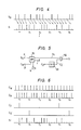
- Fig. 4 is a time chart which explains an embodiment of the present invention. The embodiment of the invention will now be described with reference to this time chart.
- a train of original digital signal pulses S0 sent from the sending terminal l are synchronized to result in a train of synchronized digital signal pulses S in which each element corresponds as indicated by arrows.
- Portions indicated by x and y in the pulse train S are synchronous portions, and other portions are synchronous portions.
- the original signal pulses S0 may be or may not be inserted in the portion x. Though the details will be described later, whether the pulses be inserted or not is determined as described below.
- the bit rate of the original signal pulse train S0 is smaller than the bit rate (strictly, the bit rate which does not include pulses with a mark y) of the synchronized signal pulse train S. Therefore, if the pulses of the original signal pulse train S0 are continued to be transferred into the synchronized signal pulse train S, the number pulses could become short of supply. That is, transfer of the pulses requires that, the pulses in the original signal pulse train S0 must lead the synchronized signal pulse train S as indicated by arrows in the drawing. The leading grade decreases with the lapse of time.
- the pulses in the original signal pulse train S0 must lead the pulses of the synchronized signal pulse train S by more than a predetermined period of time to maintain margin.
- the leading grade becomes smaller than a predetermined value, therefore, the transfer of pulse into the portion x is omitted one time (a portion of arrow J in Fig. 4). This makes it possible to increase the leading grade and to continue the transfer operation with sufficient margin.
- the original signal pulse train S0 shown in Fig. 4 is applied to an input terminal 0 of a buffer memory (BM) 5l of Fig. 5.
- the signals are written onto the buffer memory 5l by write pulses C W .
- the written pulses are read by read pulses C R applied to a terminal q of the buffer memory 5l. How to produce the read pulses C R will be described later.
- the signals are not read at time point y, the signals are read at time point x when the leading grade is great, and the signals are not read at time point x when the leading grade is small.
- the read signals S1 are synthesized with the read indication pulses C2′ through an OR gate 52 thereby to obtain a synchronized signal pulse train S in an encoded form.
- the read indication pulse C2′ is obtained as described below. That is, the pulse train C2 of Fig. 6 has a mark (with pulse) when the pulse is to be transferred at time point x in the read pulse train C R and has a space without pulse) when the pulse is not to be transferred.
- the pulse train C2 is delayed to a position y by a delay line 53 of Fig. 5 to obtain a read indication pulse train C2′. Thus, there is indicated whether the pulse is "transferred” or "not transferred".
- the read pulse train C R and the pulse train C2 of Fig. 6 can be obtained by using "empty" pulses E sent from the buffer memory 5l of Fig. 5. This will be described with reference to Figs. 7 and 8.
- the original signals S0 are written onto the buffer memory 5l of Fig. 5 using the write pulse train C W of Fig. 7 and are read out using the write pulse train C R of Fig. 7. As described earlier, in this case, the write pulses C W must lead the read pulses C R with sufficient margin.
- Whether the pulse be read or not at the portion marked with x in the read pulse train C R of Fig. 7 is determined depending upon the degree of margin. This will be described below in further detail.
- a signal E of Fig. 7 represents the case where the buffer memory contains one signal or less signal at every moment in the read pulse train C R of Fig. 7.
- a section of mark indicates this fact which is produced as an "empry" signal E from the terminal of the buffer memory 5l of Fig. 5.
- the pulse train C2 is synthesized with the pulse train C0 of Fig. 7 through an OR circuit 82 to obtain the read pulse train C R .
- Fig. 8 shows an embodiment for putting this operation into practice.
- the signal format converter 4 which receives the thus coded pulse train S and demodulates it into the original pulse train will now be described with reference to Figs. 9 to ll.
- the received pulse train S′ is applied to an input terminal b′. Portions marked with y in the pulse train S′ are sampled by an AND gate 9l. A pulse train C1′ for sampling is added to an input terminal m′. As a result, there is obtained a pulse train C2". If the pulse train C2" and a pulse train C0′ are synthesized together through an AND gate 92, there is obtained a write pulse train C W ′. Using the write pulse train C W ′, the pulse train S" delayed by a delay line 93 by a time t is written onto a buffer memory 94. In this case, signals of the pulse train S" corresponding to y1, x2, y2 and y3 are not written. The read pulses C R ′ written onto the buffer memory 94 are successively read out, and are converted into demodulated signals S0".
- the phase is deviated one bit by one bit repetitively until the pulses are brought back into synchronism, in order to obtain the pulse trains C1′ and C0′.
- a frequency locked loop 95 which convertes the write pulses C W ′ into the read pulses C R ′ of Fig. 9 is constructed as shown in Fig. ll.
- a counter lll counts the clock rate of the write pulses C W ′.
- a counter ll2 counts the clock rate of a built-in clock ll5.
- a comparator ll3 compares the result of the counter lll with the result of the counter ll2, and subtracts a pulse via a gate ll4 when the clock rate of the built-in clock ll5 is faster than the above clock rate. Owing to the above operation,time distances between the write pulses C W ′ are averaged to generate read pulses C R ′.
- the above embodiment has dealt with the case where the synchronous portions and the asynchronous portions of the coded pulse train has a ratio of 3 to l. However, this ratio can be changed depending upon the situations. The efficiency increases with the increase in the ratio of the synchronous portions. Further, the pulse train can be synchronized into any bit rate by increasing the ratio of the asynchronous portions or by leaving unused pulses in the synchronous portions.
- the number of coding digits in the asynchronous portions was two,consisting of x and y.
- the number of coding digits may be increased so that the signals are little affected by errors.
Landscapes
- Engineering & Computer Science (AREA)
- Signal Processing (AREA)
- Multimedia (AREA)
- Computer Networks & Wireless Communication (AREA)
- Power Engineering (AREA)
- Time-Division Multiplex Systems (AREA)
- Synchronisation In Digital Transmission Systems (AREA)
Applications Claiming Priority (2)
| Application Number | Priority Date | Filing Date | Title |
|---|---|---|---|
| JP60228675A JPH0697759B2 (ja) | 1985-10-16 | 1985-10-16 | デジタル信号の同期化方式 |
| JP228675/85 | 1985-10-16 |
Publications (3)
| Publication Number | Publication Date |
|---|---|
| EP0219016A2 true EP0219016A2 (de) | 1987-04-22 |
| EP0219016A3 EP0219016A3 (en) | 1989-06-21 |
| EP0219016B1 EP0219016B1 (de) | 1993-01-07 |
Family
ID=16880049
Family Applications (1)
| Application Number | Title | Priority Date | Filing Date |
|---|---|---|---|
| EP86113710A Expired - Lifetime EP0219016B1 (de) | 1985-10-16 | 1986-10-03 | Digitales Übertragungssystem mit Signalrateumsetzung |
Country Status (5)
| Country | Link |
|---|---|
| US (1) | US4796281A (de) |
| EP (1) | EP0219016B1 (de) |
| JP (1) | JPH0697759B2 (de) |
| CA (1) | CA1255004A (de) |
| DE (1) | DE3687439T2 (de) |
Cited By (1)
| Publication number | Priority date | Publication date | Assignee | Title |
|---|---|---|---|---|
| FR2627338A1 (fr) * | 1988-02-17 | 1989-08-18 | Chezelles Gilles De | Procede et appareil de transmission de donnees depuis un systeme emetteur jusqu'a un systeme recepteur |
Families Citing this family (3)
| Publication number | Priority date | Publication date | Assignee | Title |
|---|---|---|---|---|
| JPH07112179B2 (ja) * | 1989-10-19 | 1995-11-29 | 日本電気株式会社 | フレーム位相同期回路 |
| US9626320B2 (en) * | 2013-09-19 | 2017-04-18 | Nvidia Corporation | Technique for scaling the bandwidth of a processing element to match the bandwidth of an interconnect |
| US9996490B2 (en) * | 2013-09-19 | 2018-06-12 | Nvidia Corporation | Technique for scaling the bandwidth of a processing element to match the bandwidth of an interconnect |
Family Cites Families (5)
| Publication number | Priority date | Publication date | Assignee | Title |
|---|---|---|---|---|
| US4025720A (en) * | 1975-05-30 | 1977-05-24 | Gte Automatic Electric Laboratories Incorporated | Digital bit rate converter |
| JPS5923660B2 (ja) * | 1979-02-19 | 1984-06-04 | 株式会社日立製作所 | ディジタル信号伝送方式 |
| US4484327A (en) * | 1983-05-02 | 1984-11-20 | The United States Of America As Represented By The Secretary Of The Army | Pulse code modulation rate converter |
| JPH069346B2 (ja) * | 1983-10-19 | 1994-02-02 | 富士通株式会社 | 同期伝送のための周波数変換方法 |
| US4661966A (en) * | 1985-09-17 | 1987-04-28 | T-Bar Incorporated | Method and apparatus for adjusting transmission rates in data channels for use in switching systems |
-
1985
- 1985-10-16 JP JP60228675A patent/JPH0697759B2/ja not_active Expired - Lifetime
-
1986
- 1986-10-03 DE DE8686113710T patent/DE3687439T2/de not_active Expired - Fee Related
- 1986-10-03 EP EP86113710A patent/EP0219016B1/de not_active Expired - Lifetime
- 1986-10-16 CA CA000520659A patent/CA1255004A/en not_active Expired
- 1986-10-16 US US06/919,458 patent/US4796281A/en not_active Expired - Fee Related
Cited By (1)
| Publication number | Priority date | Publication date | Assignee | Title |
|---|---|---|---|---|
| FR2627338A1 (fr) * | 1988-02-17 | 1989-08-18 | Chezelles Gilles De | Procede et appareil de transmission de donnees depuis un systeme emetteur jusqu'a un systeme recepteur |
Also Published As
| Publication number | Publication date |
|---|---|
| EP0219016A3 (en) | 1989-06-21 |
| JPH0697759B2 (ja) | 1994-11-30 |
| EP0219016B1 (de) | 1993-01-07 |
| JPS6290047A (ja) | 1987-04-24 |
| CA1255004A (en) | 1989-05-30 |
| US4796281A (en) | 1989-01-03 |
| DE3687439T2 (de) | 1993-05-06 |
| DE3687439D1 (de) | 1993-02-18 |
Similar Documents
| Publication | Publication Date | Title |
|---|---|---|
| EP0460751B1 (de) | Verfahren zum Übertragen von Bild- und/oder Tonsignalen | |
| US4818995A (en) | Parallel transmission system | |
| US5138440A (en) | Method and apparatus for communicating a plurality of asynchronous signals over a digital communication path | |
| US5353313A (en) | Transmission of a clock signal over an asynchronous data channel | |
| US4224473A (en) | TDMA Multiplexer-demultiplexer with multiple ports | |
| JPH0710058B2 (ja) | マルチプレクサとデマルチプレクサを有する高度デジタル通信系 | |
| US4410980A (en) | Time division multiplexing system | |
| EP0076505B1 (de) | Digitales Übertragungssystem | |
| EP0219016A2 (de) | Digitales Übertragungssystem mit Signalrateumsetzung | |
| JPS6087539A (ja) | 周波数変換同期伝送方式 | |
| EP0337563A1 (de) | Videosignalübertragungssystem mit anpassungsfähiger Codewortzuordnung sowie für das System geeigneter Sender und Empfänger | |
| JPH027229B2 (de) | ||
| EP1178636B1 (de) | Verfahren zur Synchrondatenübertragung | |
| JPH0546130B2 (de) | ||
| US5940437A (en) | System and method for reducing the peak load on the processor of a block processing modem | |
| JP2894705B2 (ja) | 同期信号多重伝送方式 | |
| JP2697629B2 (ja) | 速度変換装置 | |
| JPH06103872B2 (ja) | 多重伝送方式 | |
| JPH0123016B2 (de) | ||
| EP0393514A3 (de) | Kanalzugriffssystem | |
| JP2890563B2 (ja) | Pcm音声符号化方法および装置 | |
| JPS5862950A (ja) | データ伝送装置 | |
| SU748896A1 (ru) | Устройство дл асинхронного сопр жени каналов св зи | |
| EP0364170A2 (de) | Serielle Übertragungsstrecke für hohe Datenraten | |
| JPS6374236A (ja) | デ−タ伝送方式 |
Legal Events
| Date | Code | Title | Description |
|---|---|---|---|
| PUAI | Public reference made under article 153(3) epc to a published international application that has entered the european phase |
Free format text: ORIGINAL CODE: 0009012 |
|
| 17P | Request for examination filed |
Effective date: 19861003 |
|
| AK | Designated contracting states |
Kind code of ref document: A2 Designated state(s): DE FR GB |
|
| PUAL | Search report despatched |
Free format text: ORIGINAL CODE: 0009013 |
|
| AK | Designated contracting states |
Kind code of ref document: A3 Designated state(s): DE FR GB |
|
| 17Q | First examination report despatched |
Effective date: 19910827 |
|
| GRAA | (expected) grant |
Free format text: ORIGINAL CODE: 0009210 |
|
| AK | Designated contracting states |
Kind code of ref document: B1 Designated state(s): DE FR GB |
|
| REF | Corresponds to: |
Ref document number: 3687439 Country of ref document: DE Date of ref document: 19930218 |
|
| ET | Fr: translation filed | ||
| PLBE | No opposition filed within time limit |
Free format text: ORIGINAL CODE: 0009261 |
|
| STAA | Information on the status of an ep patent application or granted ep patent |
Free format text: STATUS: NO OPPOSITION FILED WITHIN TIME LIMIT |
|
| 26N | No opposition filed | ||
| PGFP | Annual fee paid to national office [announced via postgrant information from national office to epo] |
Ref country code: DE Payment date: 19941124 Year of fee payment: 9 |
|
| PG25 | Lapsed in a contracting state [announced via postgrant information from national office to epo] |
Ref country code: DE Effective date: 19960702 |
|
| PGFP | Annual fee paid to national office [announced via postgrant information from national office to epo] |
Ref country code: GB Payment date: 19970923 Year of fee payment: 12 |
|
| PGFP | Annual fee paid to national office [announced via postgrant information from national office to epo] |
Ref country code: FR Payment date: 19971017 Year of fee payment: 12 |
|
| PG25 | Lapsed in a contracting state [announced via postgrant information from national office to epo] |
Ref country code: GB Free format text: LAPSE BECAUSE OF NON-PAYMENT OF DUE FEES Effective date: 19981003 |
|
| GBPC | Gb: european patent ceased through non-payment of renewal fee |
Effective date: 19981003 |
|
| PG25 | Lapsed in a contracting state [announced via postgrant information from national office to epo] |
Ref country code: FR Free format text: LAPSE BECAUSE OF NON-PAYMENT OF DUE FEES Effective date: 19990630 |
|
| REG | Reference to a national code |
Ref country code: FR Ref legal event code: ST |