EP0219122B1 - Metallisiertes Keramiksubstrat und Herstellungsverfahren - Google Patents
Metallisiertes Keramiksubstrat und Herstellungsverfahren Download PDFInfo
- Publication number
- EP0219122B1 EP0219122B1 EP19860114283 EP86114283A EP0219122B1 EP 0219122 B1 EP0219122 B1 EP 0219122B1 EP 19860114283 EP19860114283 EP 19860114283 EP 86114283 A EP86114283 A EP 86114283A EP 0219122 B1 EP0219122 B1 EP 0219122B1
- Authority
- EP
- European Patent Office
- Prior art keywords
- ceramic substrate
- substrate
- aluminum nitride
- metallic layer
- nitride ceramic
- Prior art date
- Legal status (The legal status is an assumption and is not a legal conclusion. Google has not performed a legal analysis and makes no representation as to the accuracy of the status listed.)
- Expired
Links
- 239000000758 substrate Substances 0.000 title description 77
- 239000000919 ceramic Substances 0.000 title description 53
- 238000004519 manufacturing process Methods 0.000 title description 10
- 239000010410 layer Substances 0.000 description 37
- 238000000034 method Methods 0.000 description 31
- PMHQVHHXPFUNSP-UHFFFAOYSA-M copper(1+);methylsulfanylmethane;bromide Chemical compound Br[Cu].CSC PMHQVHHXPFUNSP-UHFFFAOYSA-M 0.000 description 22
- PXHVJJICTQNCMI-UHFFFAOYSA-N Nickel Chemical compound [Ni] PXHVJJICTQNCMI-UHFFFAOYSA-N 0.000 description 20
- HEMHJVSKTPXQMS-UHFFFAOYSA-M Sodium hydroxide Chemical compound [OH-].[Na+] HEMHJVSKTPXQMS-UHFFFAOYSA-M 0.000 description 18
- 238000007772 electroless plating Methods 0.000 description 18
- 239000000243 solution Substances 0.000 description 13
- XLYOFNOQVPJJNP-UHFFFAOYSA-N water Substances O XLYOFNOQVPJJNP-UHFFFAOYSA-N 0.000 description 13
- 239000011148 porous material Substances 0.000 description 12
- 229910052751 metal Inorganic materials 0.000 description 11
- 239000002184 metal Substances 0.000 description 11
- 229910052759 nickel Inorganic materials 0.000 description 10
- 238000005406 washing Methods 0.000 description 8
- RYGMFSIKBFXOCR-UHFFFAOYSA-N Copper Chemical compound [Cu] RYGMFSIKBFXOCR-UHFFFAOYSA-N 0.000 description 7
- 239000003513 alkali Substances 0.000 description 7
- 229910052802 copper Inorganic materials 0.000 description 7
- 239000010949 copper Substances 0.000 description 7
- 239000010408 film Substances 0.000 description 7
- 238000007747 plating Methods 0.000 description 6
- 239000003054 catalyst Substances 0.000 description 5
- LFQSCWFLJHTTHZ-UHFFFAOYSA-N Ethanol Chemical compound CCO LFQSCWFLJHTTHZ-UHFFFAOYSA-N 0.000 description 4
- KWYUFKZDYYNOTN-UHFFFAOYSA-M Potassium hydroxide Chemical compound [OH-].[K+] KWYUFKZDYYNOTN-UHFFFAOYSA-M 0.000 description 4
- 238000005530 etching Methods 0.000 description 4
- WMFOQBRAJBCJND-UHFFFAOYSA-M Lithium hydroxide Chemical compound [Li+].[OH-] WMFOQBRAJBCJND-UHFFFAOYSA-M 0.000 description 3
- 238000007598 dipping method Methods 0.000 description 3
- 150000002739 metals Chemical class 0.000 description 3
- 239000010409 thin film Substances 0.000 description 3
- QGZKDVFQNNGYKY-UHFFFAOYSA-N Ammonia Chemical compound N QGZKDVFQNNGYKY-UHFFFAOYSA-N 0.000 description 2
- XEEYBQQBJWHFJM-UHFFFAOYSA-N Iron Chemical compound [Fe] XEEYBQQBJWHFJM-UHFFFAOYSA-N 0.000 description 2
- 206010070834 Sensitisation Diseases 0.000 description 2
- 238000001994 activation Methods 0.000 description 2
- 239000007864 aqueous solution Substances 0.000 description 2
- 238000007796 conventional method Methods 0.000 description 2
- 239000002003 electrode paste Substances 0.000 description 2
- 238000009713 electroplating Methods 0.000 description 2
- 239000000203 mixture Substances 0.000 description 2
- 238000004806 packaging method and process Methods 0.000 description 2
- 238000001556 precipitation Methods 0.000 description 2
- 230000008313 sensitization Effects 0.000 description 2
- 238000005245 sintering Methods 0.000 description 2
- VYZAMTAEIAYCRO-UHFFFAOYSA-N Chromium Chemical compound [Cr] VYZAMTAEIAYCRO-UHFFFAOYSA-N 0.000 description 1
- BQCADISMDOOEFD-UHFFFAOYSA-N Silver Chemical compound [Ag] BQCADISMDOOEFD-UHFFFAOYSA-N 0.000 description 1
- UIIMBOGNXHQVGW-UHFFFAOYSA-M Sodium bicarbonate Chemical class [Na+].OC([O-])=O UIIMBOGNXHQVGW-UHFFFAOYSA-M 0.000 description 1
- 230000002378 acidificating effect Effects 0.000 description 1
- 230000004913 activation Effects 0.000 description 1
- 239000000654 additive Substances 0.000 description 1
- 230000000996 additive effect Effects 0.000 description 1
- 229910052783 alkali metal Inorganic materials 0.000 description 1
- 150000001340 alkali metals Chemical class 0.000 description 1
- 229910052784 alkaline earth metal Inorganic materials 0.000 description 1
- PNEYBMLMFCGWSK-UHFFFAOYSA-N aluminium oxide Inorganic materials [O-2].[O-2].[O-2].[Al+3].[Al+3] PNEYBMLMFCGWSK-UHFFFAOYSA-N 0.000 description 1
- 150000001412 amines Chemical class 0.000 description 1
- 229910021529 ammonia Inorganic materials 0.000 description 1
- QVGXLLKOCUKJST-UHFFFAOYSA-N atomic oxygen Chemical compound [O] QVGXLLKOCUKJST-UHFFFAOYSA-N 0.000 description 1
- 150000004649 carbonic acid derivatives Chemical class 0.000 description 1
- 229910010293 ceramic material Inorganic materials 0.000 description 1
- 229910052804 chromium Inorganic materials 0.000 description 1
- 239000011651 chromium Substances 0.000 description 1
- 239000004020 conductor Substances 0.000 description 1
- 238000005238 degreasing Methods 0.000 description 1
- 238000000151 deposition Methods 0.000 description 1
- 230000008021 deposition Effects 0.000 description 1
- 238000009792 diffusion process Methods 0.000 description 1
- 230000000694 effects Effects 0.000 description 1
- 239000011521 glass Substances 0.000 description 1
- PCHJSUWPFVWCPO-UHFFFAOYSA-N gold Chemical compound [Au] PCHJSUWPFVWCPO-UHFFFAOYSA-N 0.000 description 1
- 229910052737 gold Inorganic materials 0.000 description 1
- 239000010931 gold Substances 0.000 description 1
- 230000007062 hydrolysis Effects 0.000 description 1
- 238000006460 hydrolysis reaction Methods 0.000 description 1
- 150000004679 hydroxides Chemical class 0.000 description 1
- 238000005342 ion exchange Methods 0.000 description 1
- 150000002500 ions Chemical class 0.000 description 1
- 229910052742 iron Inorganic materials 0.000 description 1
- WABPQHHGFIMREM-UHFFFAOYSA-N lead(0) Chemical compound [Pb] WABPQHHGFIMREM-UHFFFAOYSA-N 0.000 description 1
- 239000000463 material Substances 0.000 description 1
- 230000007935 neutral effect Effects 0.000 description 1
- 229910052760 oxygen Inorganic materials 0.000 description 1
- 239000001301 oxygen Substances 0.000 description 1
- 239000011347 resin Substances 0.000 description 1
- 229920005989 resin Polymers 0.000 description 1
- 238000007650 screen-printing Methods 0.000 description 1
- 239000004065 semiconductor Substances 0.000 description 1
- 229910052709 silver Inorganic materials 0.000 description 1
- 239000004332 silver Substances 0.000 description 1
- 235000017557 sodium bicarbonate Nutrition 0.000 description 1
- 238000004544 sputter deposition Methods 0.000 description 1
- 239000002344 surface layer Substances 0.000 description 1
Images


Classifications
-
- C—CHEMISTRY; METALLURGY
- C04—CEMENTS; CONCRETE; ARTIFICIAL STONE; CERAMICS; REFRACTORIES
- C04B—LIME, MAGNESIA; SLAG; CEMENTS; COMPOSITIONS THEREOF, e.g. MORTARS, CONCRETE OR LIKE BUILDING MATERIALS; ARTIFICIAL STONE; CERAMICS; REFRACTORIES; TREATMENT OF NATURAL STONE
- C04B41/00—After-treatment of mortars, concrete, artificial stone or ceramics; Treatment of natural stone
- C04B41/009—After-treatment of mortars, concrete, artificial stone or ceramics; Treatment of natural stone characterised by the material treated
-
- C—CHEMISTRY; METALLURGY
- C04—CEMENTS; CONCRETE; ARTIFICIAL STONE; CERAMICS; REFRACTORIES
- C04B—LIME, MAGNESIA; SLAG; CEMENTS; COMPOSITIONS THEREOF, e.g. MORTARS, CONCRETE OR LIKE BUILDING MATERIALS; ARTIFICIAL STONE; CERAMICS; REFRACTORIES; TREATMENT OF NATURAL STONE
- C04B41/00—After-treatment of mortars, concrete, artificial stone or ceramics; Treatment of natural stone
- C04B41/53—After-treatment of mortars, concrete, artificial stone or ceramics; Treatment of natural stone involving the removal of at least part of the materials of the treated article, e.g. etching, drying of hardened concrete
-
- C—CHEMISTRY; METALLURGY
- C04—CEMENTS; CONCRETE; ARTIFICIAL STONE; CERAMICS; REFRACTORIES
- C04B—LIME, MAGNESIA; SLAG; CEMENTS; COMPOSITIONS THEREOF, e.g. MORTARS, CONCRETE OR LIKE BUILDING MATERIALS; ARTIFICIAL STONE; CERAMICS; REFRACTORIES; TREATMENT OF NATURAL STONE
- C04B41/00—After-treatment of mortars, concrete, artificial stone or ceramics; Treatment of natural stone
- C04B41/80—After-treatment of mortars, concrete, artificial stone or ceramics; Treatment of natural stone of only ceramics
- C04B41/91—After-treatment of mortars, concrete, artificial stone or ceramics; Treatment of natural stone of only ceramics involving the removal of part of the materials of the treated articles, e.g. etching
-
- H—ELECTRICITY
- H05—ELECTRIC TECHNIQUES NOT OTHERWISE PROVIDED FOR
- H05K—PRINTED CIRCUITS; CASINGS OR CONSTRUCTIONAL DETAILS OF ELECTRIC APPARATUS; MANUFACTURE OF ASSEMBLAGES OF ELECTRICAL COMPONENTS
- H05K1/00—Printed circuits
- H05K1/02—Details
- H05K1/03—Use of materials for the substrate
- H05K1/0306—Inorganic insulating substrates, e.g. ceramic, glass
-
- H—ELECTRICITY
- H05—ELECTRIC TECHNIQUES NOT OTHERWISE PROVIDED FOR
- H05K—PRINTED CIRCUITS; CASINGS OR CONSTRUCTIONAL DETAILS OF ELECTRIC APPARATUS; MANUFACTURE OF ASSEMBLAGES OF ELECTRICAL COMPONENTS
- H05K3/00—Apparatus or processes for manufacturing printed circuits
- H05K3/10—Apparatus or processes for manufacturing printed circuits in which conductive material is applied to the insulating support in such a manner as to form the desired conductive pattern
- H05K3/18—Apparatus or processes for manufacturing printed circuits in which conductive material is applied to the insulating support in such a manner as to form the desired conductive pattern using precipitation techniques to apply the conductive material
- H05K3/181—Apparatus or processes for manufacturing printed circuits in which conductive material is applied to the insulating support in such a manner as to form the desired conductive pattern using precipitation techniques to apply the conductive material by electroless plating
-
- H—ELECTRICITY
- H05—ELECTRIC TECHNIQUES NOT OTHERWISE PROVIDED FOR
- H05K—PRINTED CIRCUITS; CASINGS OR CONSTRUCTIONAL DETAILS OF ELECTRIC APPARATUS; MANUFACTURE OF ASSEMBLAGES OF ELECTRICAL COMPONENTS
- H05K3/00—Apparatus or processes for manufacturing printed circuits
- H05K3/38—Improvement of the adhesion between the insulating substrate and the metal
- H05K3/381—Improvement of the adhesion between the insulating substrate and the metal by special treatment of the substrate
Definitions
- the present invention relates to a ceramic substrate on the surface of which a metallic layer is formed (metalized ceramic substrate), and a method of manufacturing the same.
- a metallic layer When a ceramic substrate is used for a circuit board of an electronic circuit, a heat sink, or an insulating substrate, a metallic layer must be formed on a ceramic layer.
- Conventional methods for forming a metallic layer on the ceramic substrate include a thin film method (e.g., sputtering or deposition), a thick film method for baking an electrode paste using screen printing, an electroless plating method, and a method in which an electrode is formed by a thin or thick film method and electrolytic plating is performed thereon.
- the metallic layer formed on the ceramic substrate has a good bonding property with respect to a ceramic substrate; (2) the metallic layer has a low electrical resistance; and (3) the metallic layer can be micropatterned.
- the metallic layer in a packaging substrate or a heat sink which mounts a high- density, high-power device, the metallic layer must be able to be bonded to the ceramic substrate without generating thermal resistance.
- the conventional methods for forming the metallic layer on the ceramic substrate cannot satisfy the above requirements, and are selectively used in accordance with applications. More specifically, for a device which requires an electrode or conductor of high precision, the thin film method is adopted. However, this method poses problems of a manufacturing cost problem and of resistance of the metallic layer since it is difficult to increase the thickness of the metallic layer with this method.
- the thick film method using an electrode paste can be carried out with low cost since it has simple procedures and allows mass production.
- a wiring has a limited precision, and an electrical resistance inherent to an electrode cannot be set to be equal to that of bulk metal, thus restricting application range of the method.
- the thin or thick film method and the electrolytic plating are combined to improve characteristics. However, this complicates manufacturing procedures, and increases cost, resulting in a limited application range.
- the conventional electroless plating technique cannot provide a sufficient peel strength between the metallic layer and the ceramic substrate.
- the ceramic substrate is preferably bonded directly to the metallic layer.
- the thick film method having a relatively high peel strength glass or oxide for maintaining a bonding property between the ceramic substrate and the metallic layer is present therebetween, resulting in a high thermal resistance.
- An aluminum nitride ceramic substrate which recently receives attention as a high heat conductivity ceramic material, cannot provide a sufficient peel strength even if the conventional thick film method is used or an oxide or an oxygen diffusion layer is formed between the metallic layer and the ceramic substrate, thus considerably increasing the thermal resistance.
- the present invention has been made in consideration of the above situation and has as its object to provide a metalized ceramic substrate in which no material preventing heat conduction is present between a metallic layer and a ceramic substrate so that the thermal resistance can be reduced, and a dense, high-purity metallic layer is formed so as to allow it to have a low electrical resistance.
- a method of manufacturing a metalized ceramic substrate comprising the steps of: treating a surface of an aluminum nitride ceramic substrate using an alkali solution; and forming a metallic layer on the treated aluminum nitride ceramic substrate by electroless plating.
- a metalized aluminum nitride ceramic substrate comprising: an aluminum nitride ceramic substrate in the surface of which a large number of small pores are formed, and in which each pore has a structure having a larger internal size than an opening size; and a metallic layer formed on a surface of the aluminum nitride ceramic substrate including the pores.
- each pore is a jar-like column or anchor whose diameter gradually increases from the surface toward the inside thereof, resulting in that a metal can be filled in the pores in the surface of the aluminum nitride ceramic substrate by electroless plating, and a metallic layer having a superior bonding property to that of the conventional structure can be formed on the aluminum nitride ceramic substrate.
- An aluminum nitride substrate prepared by a normal sintering method was subjected to ultrasonic washing in ethanol for 10 minutes.
- the substrate was dipped in an aqueous sodium hydroxide solution adjusted to a concentration of 1 mo)/dm3 at a room temperature for a predetermined period of time.
- the substrate was washed with water, and was dipped in a commercially available one- pack type catalyst (e.g., HS-101 B available from HITACHI KASEI CO.) for four minutes.
- a commercially available one- pack type catalyst e.g., HS-101 B available from HITACHI KASEI CO.
- the substrate was washed with water, it was dipped in a promoter (e.g., ADP-101 available from HITACHI KASEI CO.) for one minute.
- a promoter e.g., ADP-101 available from HITACHI KASEI CO.
- the substrate was washed with water and was dipped in a nickel electroless plating bath having the composition shown in Table 1 below, thus performing nickel electroless plating.
- the substrate was dipped in the plating bath for 80 minutes to have a plating thickness of about 2 ⁇ .Lm from the surface of the substrate and to fill pores formed in the surface of the substrate, thereby allowing precipitation of nickel.
- the substrate was then washed with water and was dried.
- the nickel plating bath was kept at a temperature of 90 ° C, the pH was adjusted to 4.0 by means of H 2 S0 4 .
- An aluminum nitride substrate prepared by a normal sintering method was subjected to ultrasonic washing in ethanol for 10 minutes.
- the substrate was dipped in an aqueous potassium hydroxide solution adjusted to a concentration of 1 moVdm3 for 60 minutes.
- the substrate was washed with water and was dipped in a commercially available one- pack type catalyst (e.g., HS-101 B available from HITACHI KASEI CO.) for four minutes.
- a commercially available one- pack type catalyst e.g., HS-101 B available from HITACHI KASEI CO.
- the substrate was dipped in a promoter (e.g., ADP-101 available from HITACHI KASEI CO.) for one minute.
- a promoter e.g., ADP-101 available from HITACHI KASEI CO.
- the substrate was washed with water and was dipped in a copper electroless plating bath having the composition shown in Table 2 below, thus performing copper electroless plating.
- the substrate was dipped in the plating bath for 80 minutes to have a plating thickness of about 2 ⁇ m from the surface of the substrate and to fill the pores formed in the surface of the substrate.
- the substrate was washed with water and then dried.
- the copper plating bath was kept at a temperature of 60 ° C, the pH was adjusted to 12.5 by means of NaOH.
- An aluminum nitride ceramic substrate prepared by a hot-press method was dipped in a degreasing alkali solution of pH 12 (e.g., CERACLEAN available from K.K. KIZAI) at a temperature of 70 ° C for a predetermined period of time. After dipping, the substrate was sufficiently washed with water, and nickel electroless plating was performed by a normal electroless plating process. In this example, a process using a commercially available electroless plating system is exemplified. After the ceramic substrate was washed with water, it was subjected to ultrasonic washing for five minutes using ion-exchange water.
- a degreasing alkali solution of pH 12 e.g., CERACLEAN available from K.K. KIZAI
- the substrate was dipped in a sensitization solution (e.g., CERASENSI available from K.K. KIZAI) at a temperature of 18 ° C to 22 ° C for five minutes.
- a catalyst additive solution e.g., ACTICERA available from K.K. KIZAI
- an activation solution e.g., CERA-ACCE available from K.K. KIZAI
- the substrate was dipped in an electroless plating solution (e.g., a NAIKO CER available from K.K. KIZAI) at a temperature of 90 ° C for one minute. After washing with water, the substrate was dried at a temperature of 150 ° C for 30 minutes. With this process, a nickel metallic film having a thickness of about 1 Ilm was formed on the aluminum nitride substrate from the surface thereof.
- an electroless plating solution e.g., a NAIKO CER available from K.K. KIZAI
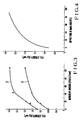
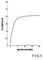
- the peel strength between the metal and ceramic was measured as follows.
- a resist was coated on the nickel or copper layer formed on the metalized aluminum nitride substrate in the above examples, and a predetermined area thereof was exposed and developed using a photomask.
- the developed substrate was dipped in a nickel or copper etching solution to form a 2 mm x 2 mm nickel or copper pad.
- a lead wire was soldered to the thus formed pad, and the peel strength was measured using a tensile machine.
- Alkalis for surface treating the aluminum nitride ceramic substrate include aqueous solutions of hydroxides, carbonates or sodium bicarbonates of alkali metals, (e.g., sodium hydroxide, potassium hydroxide, lithium hydroxide, and the like) or of alkali earth metals, and alkali aqueous solutions having an alkaline property, e.g., ammonia, amine, and the like.
- alkali metals e.g., sodium hydroxide, potassium hydroxide, lithium hydroxide, and the like
- alkali earth metals e.g., sodium hydroxide, potassium hydroxide, lithium hydroxide, and the like
- alkali aqueous solutions having an alkaline property e.g., ammonia, amine, and the like.
- any one of acidic, alkaline, and neutral baths can be used.
- Metals include all the metals which are capable of electroless plating, e.g., silver, gold, chrom
- electroless plating is performed using catalyst processes, e.g., a sensitization process, an activation process, an activator-accelerator method, and the like generally used in electroless plating.
- catalyst processes e.g., a sensitization process, an activation process, an activator-accelerator method, and the like generally used in electroless plating.
- a peel strength of 2 kg/mm 2 or higher could be realized.
- the metalized aluminum nitride ceramic substrate has very high peel strength between metal and ceramic due to an anchor effect.
- a micro circuit pattern can be formed as in a thin film method by an etching method using a photosensitive resin. Since no intermediate layer is present, a decrease in peel strength due to etching will not occur.
- the metallic layer consists of an identical metal.
- anchors and a surface layer can consist of different metals.
Landscapes
- Chemical & Material Sciences (AREA)
- Engineering & Computer Science (AREA)
- Ceramic Engineering (AREA)
- Materials Engineering (AREA)
- Structural Engineering (AREA)
- Organic Chemistry (AREA)
- Chemically Coating (AREA)
- Manufacturing Of Printed Wiring (AREA)
Claims (3)
Applications Claiming Priority (4)
| Application Number | Priority Date | Filing Date | Title |
|---|---|---|---|
| JP23025985A JPS6288394A (ja) | 1985-10-15 | 1985-10-15 | 窒化アルミニウムセラミツク基板の製造方法 |
| JP230259/85 | 1985-10-15 | ||
| JP230258/85 | 1985-10-15 | ||
| JP23025885A JPS6288392A (ja) | 1985-10-15 | 1985-10-15 | セラミツク基板 |
Publications (3)
| Publication Number | Publication Date |
|---|---|
| EP0219122A2 EP0219122A2 (de) | 1987-04-22 |
| EP0219122A3 EP0219122A3 (en) | 1988-01-07 |
| EP0219122B1 true EP0219122B1 (de) | 1990-07-04 |
Family
ID=26529241
Family Applications (1)
| Application Number | Title | Priority Date | Filing Date |
|---|---|---|---|
| EP19860114283 Expired EP0219122B1 (de) | 1985-10-15 | 1986-10-15 | Metallisiertes Keramiksubstrat und Herstellungsverfahren |
Country Status (2)
| Country | Link |
|---|---|
| EP (1) | EP0219122B1 (de) |
| DE (1) | DE3672441D1 (de) |
Cited By (1)
| Publication number | Priority date | Publication date | Assignee | Title |
|---|---|---|---|---|
| DE4138214A1 (de) * | 1991-11-21 | 1993-05-27 | Daimler Benz Ag | Verfahren zur metallisierung von aluminiumnitridkeramik |
Families Citing this family (4)
| Publication number | Priority date | Publication date | Assignee | Title |
|---|---|---|---|---|
| JPS63260884A (ja) * | 1987-04-16 | 1988-10-27 | 日本碍子株式会社 | セラミツク基体およびその製造方法 |
| DE102019216605A1 (de) * | 2019-10-29 | 2021-04-29 | Fraunhofer-Gesellschaft zur Förderung der angewandten Forschung e.V. | Formschlüssiger und/oder kraftschlüssiger Materialverbund |
| CN111592382B (zh) * | 2020-04-26 | 2021-12-17 | 江苏富乐德半导体科技有限公司 | 一种氮化铝陶瓷基板表面粗化方法 |
| CN114560705B (zh) * | 2022-01-19 | 2023-01-24 | 福建华清电子材料科技有限公司 | 一种不研磨氮化铝陶瓷基板的制备方法 |
Family Cites Families (2)
| Publication number | Priority date | Publication date | Assignee | Title |
|---|---|---|---|---|
| DE3150399A1 (de) * | 1981-12-15 | 1983-07-21 | Schering Ag, 1000 Berlin Und 4619 Bergkamen | Verfahren zur haftfesten metallisierung von keramischen materialien |
| US4604299A (en) * | 1983-06-09 | 1986-08-05 | Kollmorgen Technologies Corporation | Metallization of ceramics |
-
1986
- 1986-10-15 DE DE8686114283T patent/DE3672441D1/de not_active Expired - Lifetime
- 1986-10-15 EP EP19860114283 patent/EP0219122B1/de not_active Expired
Cited By (1)
| Publication number | Priority date | Publication date | Assignee | Title |
|---|---|---|---|---|
| DE4138214A1 (de) * | 1991-11-21 | 1993-05-27 | Daimler Benz Ag | Verfahren zur metallisierung von aluminiumnitridkeramik |
Also Published As
| Publication number | Publication date |
|---|---|
| EP0219122A3 (en) | 1988-01-07 |
| DE3672441D1 (de) | 1990-08-09 |
| EP0219122A2 (de) | 1987-04-22 |
Similar Documents
| Publication | Publication Date | Title |
|---|---|---|
| KR102387227B1 (ko) | 금속/세라믹 회로 기판 제조 방법 | |
| US5058799A (en) | Metallized ceramic substrate and method therefor | |
| US5100714A (en) | Metallized ceramic substrate and method therefor | |
| EP0219122B1 (de) | Metallisiertes Keramiksubstrat und Herstellungsverfahren | |
| JP3208438B2 (ja) | 金属層を備えたセラミックス基板とその製造方法 | |
| JPS594062A (ja) | 電子部品外囲器及びその製造方法 | |
| JPH0322715B2 (de) | ||
| JPH0410752B2 (de) | ||
| JP3244102B2 (ja) | Icパッケージ | |
| JP3846708B2 (ja) | 電子部品のめっき方法、及び電子部品の製造方法 | |
| JPH1065294A (ja) | セラミックス配線基板およびその製造方法 | |
| JP3801334B2 (ja) | 半導体素子搭載用基板とその製造方法 | |
| JP3645744B2 (ja) | セラミック配線基板 | |
| JP3089961B2 (ja) | セラミック基板の銅メタライズ法 | |
| JP2591649B2 (ja) | セラミック基板表面に金属層を形成する方法 | |
| JPS622591A (ja) | 金属ベ−ス混成集積回路基板の製法 | |
| JPH0222992Y2 (de) | ||
| JPS60107845A (ja) | 半導体用回路基板 | |
| JP3583018B2 (ja) | セラミック配線基板 | |
| EP0254201A1 (de) | Verfahren zum Metallisieren von keramischen Substraten | |
| JPH08274123A (ja) | 混成集積回路基板用導体の製造方法 | |
| JP2720063B2 (ja) | 配線基板の製造方法 | |
| JPH08102578A (ja) | セラミックプリント配線板及びその製造方法 | |
| JPS61256688A (ja) | 回路基板の製造方法 | |
| Fudala et al. | The performance and reliability of a new plated copper technology on ceramic |
Legal Events
| Date | Code | Title | Description |
|---|---|---|---|
| PUAI | Public reference made under article 153(3) epc to a published international application that has entered the european phase |
Free format text: ORIGINAL CODE: 0009012 |
|
| 17P | Request for examination filed |
Effective date: 19861015 |
|
| AK | Designated contracting states |
Kind code of ref document: A2 Designated state(s): DE FR |
|
| PUAL | Search report despatched |
Free format text: ORIGINAL CODE: 0009013 |
|
| AK | Designated contracting states |
Kind code of ref document: A3 Designated state(s): DE FR |
|
| 17Q | First examination report despatched |
Effective date: 19891102 |
|
| GRAA | (expected) grant |
Free format text: ORIGINAL CODE: 0009210 |
|
| AK | Designated contracting states |
Kind code of ref document: B1 Designated state(s): DE FR |
|
| REF | Corresponds to: |
Ref document number: 3672441 Country of ref document: DE Date of ref document: 19900809 |
|
| ET | Fr: translation filed | ||
| PLBE | No opposition filed within time limit |
Free format text: ORIGINAL CODE: 0009261 |
|
| STAA | Information on the status of an ep patent application or granted ep patent |
Free format text: STATUS: NO OPPOSITION FILED WITHIN TIME LIMIT |
|
| 26N | No opposition filed | ||
| PGFP | Annual fee paid to national office [announced via postgrant information from national office to epo] |
Ref country code: FR Payment date: 20051010 Year of fee payment: 20 |
|
| PGFP | Annual fee paid to national office [announced via postgrant information from national office to epo] |
Ref country code: DE Payment date: 20051014 Year of fee payment: 20 |