EP0219401A1 - Polariseur par absorption différentielle, son procédé de réalisation, et dispositif mettant en oeuvre ledit procédé - Google Patents
Polariseur par absorption différentielle, son procédé de réalisation, et dispositif mettant en oeuvre ledit procédé Download PDFInfo
- Publication number
- EP0219401A1 EP0219401A1 EP86402087A EP86402087A EP0219401A1 EP 0219401 A1 EP0219401 A1 EP 0219401A1 EP 86402087 A EP86402087 A EP 86402087A EP 86402087 A EP86402087 A EP 86402087A EP 0219401 A1 EP0219401 A1 EP 0219401A1
- Authority
- EP
- European Patent Office
- Prior art keywords
- layer
- dielectric
- polarizer according
- face
- dielectric material
- Prior art date
- Legal status (The legal status is an assumption and is not a legal conclusion. Google has not performed a legal analysis and makes no representation as to the accuracy of the status listed.)
- Granted
Links
- 238000010521 absorption reaction Methods 0.000 title claims abstract description 27
- 238000000034 method Methods 0.000 title claims abstract description 18
- 238000004519 manufacturing process Methods 0.000 title claims description 4
- 239000003989 dielectric material Substances 0.000 claims abstract description 22
- 230000010287 polarization Effects 0.000 claims abstract description 15
- 239000000758 substrate Substances 0.000 claims abstract description 11
- 239000000463 material Substances 0.000 claims description 18
- 150000002500 ions Chemical class 0.000 claims description 13
- 239000007788 liquid Substances 0.000 claims description 12
- 238000000151 deposition Methods 0.000 claims description 11
- 230000008021 deposition Effects 0.000 claims description 10
- RTAQQCXQSZGOHL-UHFFFAOYSA-N Titanium Chemical compound [Ti] RTAQQCXQSZGOHL-UHFFFAOYSA-N 0.000 claims description 7
- 238000003754 machining Methods 0.000 claims description 7
- 125000002524 organometallic group Chemical group 0.000 claims description 6
- 238000010884 ion-beam technique Methods 0.000 claims description 5
- 239000010936 titanium Substances 0.000 claims description 5
- 229910052719 titanium Inorganic materials 0.000 claims description 5
- 238000010438 heat treatment Methods 0.000 claims description 4
- 230000000873 masking effect Effects 0.000 claims description 4
- 239000007769 metal material Substances 0.000 claims description 4
- 239000010703 silicon Substances 0.000 claims description 4
- 229910052710 silicon Inorganic materials 0.000 claims description 4
- 230000008020 evaporation Effects 0.000 claims description 3
- 238000001704 evaporation Methods 0.000 claims description 3
- 238000009432 framing Methods 0.000 claims description 3
- WFKWXMTUELFFGS-UHFFFAOYSA-N tungsten Chemical compound [W] WFKWXMTUELFFGS-UHFFFAOYSA-N 0.000 claims description 3
- 229910052721 tungsten Inorganic materials 0.000 claims description 3
- 239000010937 tungsten Substances 0.000 claims description 3
- VYPSYNLAJGMNEJ-UHFFFAOYSA-N Silicium dioxide Chemical compound O=[Si]=O VYPSYNLAJGMNEJ-UHFFFAOYSA-N 0.000 claims 2
- GWEVSGVZZGPLCZ-UHFFFAOYSA-N Titan oxide Chemical compound O=[Ti]=O GWEVSGVZZGPLCZ-UHFFFAOYSA-N 0.000 claims 1
- 239000000203 mixture Substances 0.000 claims 1
- 230000003647 oxidation Effects 0.000 claims 1
- 238000007254 oxidation reaction Methods 0.000 claims 1
- 239000000377 silicon dioxide Substances 0.000 claims 1
- OGIDPMRJRNCKJF-UHFFFAOYSA-N titanium oxide Inorganic materials [Ti]=O OGIDPMRJRNCKJF-UHFFFAOYSA-N 0.000 claims 1
- 239000012071 phase Substances 0.000 description 7
- 230000003287 optical effect Effects 0.000 description 6
- 230000005540 biological transmission Effects 0.000 description 5
- XUIMIQQOPSSXEZ-UHFFFAOYSA-N Silicon Chemical compound [Si] XUIMIQQOPSSXEZ-UHFFFAOYSA-N 0.000 description 3
- 230000000694 effects Effects 0.000 description 3
- XKRFYHLGVUSROY-UHFFFAOYSA-N Argon Chemical compound [Ar] XKRFYHLGVUSROY-UHFFFAOYSA-N 0.000 description 2
- 230000008030 elimination Effects 0.000 description 2
- 238000003379 elimination reaction Methods 0.000 description 2
- 230000001788 irregular Effects 0.000 description 2
- 229910052751 metal Inorganic materials 0.000 description 2
- 239000002184 metal Substances 0.000 description 2
- SIWVEOZUMHYXCS-UHFFFAOYSA-N oxo(oxoyttriooxy)yttrium Chemical compound O=[Y]O[Y]=O SIWVEOZUMHYXCS-UHFFFAOYSA-N 0.000 description 2
- 241001080024 Telles Species 0.000 description 1
- 238000013459 approach Methods 0.000 description 1
- 229910052786 argon Inorganic materials 0.000 description 1
- 239000013078 crystal Substances 0.000 description 1
- 239000002178 crystalline material Substances 0.000 description 1
- 238000010586 diagram Methods 0.000 description 1
- 238000005530 etching Methods 0.000 description 1
- 238000002474 experimental method Methods 0.000 description 1
- 239000007789 gas Substances 0.000 description 1
- 238000001534 heteroepitaxy Methods 0.000 description 1
- 238000011065 in-situ storage Methods 0.000 description 1
- 230000003993 interaction Effects 0.000 description 1
- 229910021645 metal ion Inorganic materials 0.000 description 1
- 238000006213 oxygenation reaction Methods 0.000 description 1
- 230000001902 propagating effect Effects 0.000 description 1
- 238000000926 separation method Methods 0.000 description 1
- 230000000699 topical effect Effects 0.000 description 1
- 238000001771 vacuum deposition Methods 0.000 description 1
- 239000012808 vapor phase Substances 0.000 description 1
Images


Classifications
-
- G—PHYSICS
- G02—OPTICS
- G02B—OPTICAL ELEMENTS, SYSTEMS OR APPARATUS
- G02B6/00—Light guides; Structural details of arrangements comprising light guides and other optical elements, e.g. couplings
- G02B6/10—Light guides; Structural details of arrangements comprising light guides and other optical elements, e.g. couplings of the optical waveguide type
- G02B6/105—Light guides; Structural details of arrangements comprising light guides and other optical elements, e.g. couplings of the optical waveguide type having optical polarisation effects
-
- G—PHYSICS
- G02—OPTICS
- G02B—OPTICAL ELEMENTS, SYSTEMS OR APPARATUS
- G02B6/00—Light guides; Structural details of arrangements comprising light guides and other optical elements, e.g. couplings
- G02B6/10—Light guides; Structural details of arrangements comprising light guides and other optical elements, e.g. couplings of the optical waveguide type
- G02B6/12—Light guides; Structural details of arrangements comprising light guides and other optical elements, e.g. couplings of the optical waveguide type of the integrated circuit kind
- G02B6/126—Light guides; Structural details of arrangements comprising light guides and other optical elements, e.g. couplings of the optical waveguide type of the integrated circuit kind using polarisation effects
-
- Y—GENERAL TAGGING OF NEW TECHNOLOGICAL DEVELOPMENTS; GENERAL TAGGING OF CROSS-SECTIONAL TECHNOLOGIES SPANNING OVER SEVERAL SECTIONS OF THE IPC; TECHNICAL SUBJECTS COVERED BY FORMER USPC CROSS-REFERENCE ART COLLECTIONS [XRACs] AND DIGESTS
- Y10—TECHNICAL SUBJECTS COVERED BY FORMER USPC
- Y10S—TECHNICAL SUBJECTS COVERED BY FORMER USPC CROSS-REFERENCE ART COLLECTIONS [XRACs] AND DIGESTS
- Y10S359/00—Optical: systems and elements
- Y10S359/90—Methods
Definitions
- the invention relates to a differential absorption polarizer making it possible in particular to produce a polarizer in integrated optics. It therefore also relates to the method for producing such a polarizer and to an apparatus implementing this method.
- the second type of polarizer leads to complex configurations, some of which are not always compatible with the planar geometry of the integrated optics.
- the use on the surface of the waveguide of an anisotropic crystal of which one of the refractive indices would be, for one of the optical polarizations, greater than the index of waveguide refraction can be found in the article "ANISOTROPIC POLARIZERS FOR Ti: LiNb03 STRIP WAVEGUIDES" by M. PAPUCHON et al published in Technical Digest on April 24-26, 1984 (KISSIMMEE, Florida 7th topical meeting INTEGRATED AND GUIDED- WAVE OPTICS-WC5).
- the anisotropy properties of the substrate itself can be used to obtain the desired effect in situ.
- the substrate itself eg LiNb03
- the optical axis is in the plane of the substrate, for certain angles, of waveguides with this optical axis, the propagation of "quasi TE" waves takes place with losses which can be very significant (7 50 dB on 10 mm demonstrated in the laboratory). This configuration can be a drawback when integrating other functions with specific characteristics.
- the invention therefore uses the elimination of one of the magnetic transverse TM or electric transverse TE polarizations by differential absorption.
- a polarization effect is obtained by creating a differential absorption between the polarized modes quasi TE and quasi TM thanks to the strong attenuation which can be induced on the TM wave, and this by using a metallic layer.
- a dielectric buffer layer must be inserted between the metal and the waveguide. The optogeometric parameters of this layer generally depend critically on the optical constants of the metal used. This is the case in particular of the thickness of the dielectric buffer layer which must be defined with great precision (about 100 A) The article by K.
- the mode to be absorbed will find in the bevelled thickness of the dielectric layer a thickness adapted to a better absorption.
- the invention provides a polarizer which is easy to produce and which makes it possible to obtain effective polarization.
- the invention also relates to a method of producing a polarizer by differential absorption comprising a first phase of depositing on a substrate a layer of guide material making it possible to guide a mode of transverse magnetic polarization of a wave, a second phase of deposition on the layer of guide material with a layer of dielectric material, a third phase of deposition on the layer of dielectric material with a layer of metallic material, characterized in that it comprises between said second and third phases, an additional phase of forming a plurality of zones inclined with respect to the surface of the layer of dielectric material.
- the invention also relates to a device for ionic attack on said dielectric layer comprising an ion gun emitting an ion beam towards said face of the dielectric layer, characterized in that it comprises a grid interposed between the ion gun and said face of the dielectric layer.
- This polarizer has on a face 10 of a substrate, a layer 2 of a guide material.
- a layer 2 of a guide material In this layer is injected, by means not shown and which depart from the scope of the invention, a light wave S having modes of transverse electric (TE) and transverse magnetic (TM). These polarization modes are orthogonal and are represented on the left of FIG. 1.
- the layer 2 is coated with a dielectric buffer layer 3 which is coated on its face 30 with a layer metallic 4.
- the refractive index nl of the guide material of the layer 2 is greater than the refractive index n0 of the substrate and greater than the refractive index n2 of the dielectric layer 3:
- the transverse magnetic component TM of the S wave is partially absorbed.
- the absorption is all the more effective as the thickness e of the layer 3 approaches a thickness e called the resonance thickness.
- the transverse magnetic component will be absorbed with a maximum of absorption in the section of the element 35 corresponding to this thickness of resonance.
- the polarizer of the invention comprises on a substrate 1 of refractive index n0, a layer of guide material 2 of index nl.
- the polarizer of FIG. 3 has a layer 3 of dielectric material one face 31 of which is common with the layer of guide material 2 and the opposite face 30 has a plurality of inclined zones such as zone 32
- the face 30 therefore has an irregular shape which provides the section of the polarizer, in the direction of propagation of an S wave, with a profile having several successive inclined zones.
- the undulations obtained are such that the minimum thickness e existing between a hollow in the face 30 and the opposite face 31, and the maximum thickness eM existing between a bump in the face 30 and the opposite face 31, surround the value of l 'thickness of resonance e_:
- Each inclined zone 32 therefore delimits a volume of dielectric material, comprised between this zone 32 and the face 31, of variable thickness framing the thickness of resonance e of the material.
- the face 31 is then metallized by a layer 4 as before.
- An S wave propagating in the waveguide layer 2 will therefore have its transverse magnetic component capable of being absorbed several times, that is to say each time it passes under an inclined area such as 32 of the dielectric layer 3.
- the curves in FIG. 4 show that for a thickness e of the dielectric layer 3, the transmission of the transverse magnetic component TM is minimal and its absorption is therefore maximal. On the other hand, the transmission of the electrical transverse component is not affected and does not undergo absorption.
- the polarizer of the invention provides improved efficiency compared to polarizers of known type.
- the surface 30 of the layer of electrical material 30 is irregular. However, according to another exemplary embodiment, it may have the appearance of a regular undulation. having a constant pitch p, or even a sinusoidal undulation, determining the minimum thicknesses e m and maximum thickness e M of the layer 3 meeting the condition:
- layer 2 can be of crystalline material of the LiNb0 3 type with a thickness of 2.5 to 3 ⁇ m.
- the forming of the layer 3 into inclined zones 32 can be done by stamping the surface 30 after preliminary heating of the liquid layer and before complete hardening of this layer.
- the forming can also be done after hardening of the layer 3, by ionic machining.
- the forming of this layer is carried out by ionic machining.
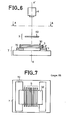
- the method of the invention providing for ionic machining of the layer 3 can be implemented by the apparatus according to the invention and represented by FIGS. 6 and 7.
- This device has a frame 7 for supporting the element to be treated.
- This frame is arranged along an axis XX '.
- the element to be treated rests on the frame 7 by shims 70 so that the face 30 of the element to be treated is substantially perpendicular to the axis XX '.
- an ion cannon makes it possible to direct an ion beam towards the face 30 of layer 3 of the element to be treated.
- a masking grid 5 made up of wires 50 of material such as tungsten is placed between the ion gun and the element to be treated, in the path of the ion beam.
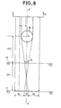
- a wire 50 placed on the ion beam diffracts this beam and provides, at a determined distance OXI from the grid, on the surface 30 of layer 3 a more or less significant attack.
- zone 37 there will be a different machining than in zones 36 and 38 and a machined surface is obtained with the grid 5 substantially of sinusoidal shape.
- a polarizer having a surface 30 having a sinusoidal ripple was produced using an ion implanter 6 operating at a high voltage of 1000 volts and providing an ion density of 0.5 mA / cm 2 with an ion source pressure of 3x10 T using Argon gas.
- the distance OX1 between the surface 30 of the layer 3 and the masking grid 5 was taken equal to 16 cm.
- the grid used consisted of rectilinear and parallel tungsten wires of 0.1 mm diameter arranged in a 0.4 mm pitch.
- the organometallic liquid used included two volumes of titanium-based liquid for one volume of silicon-based liquid.
Landscapes
- Physics & Mathematics (AREA)
- General Physics & Mathematics (AREA)
- Optics & Photonics (AREA)
- Engineering & Computer Science (AREA)
- Microelectronics & Electronic Packaging (AREA)
- Polarising Elements (AREA)
- Optical Integrated Circuits (AREA)
Abstract
Description
- L'invention concerne un polariseur par absorption différentielle permettant notamment de réaliser un polariseur en optique intégrée. Elle concerne donc également le procédé de réalisation d'un tel polariseur et un appareil mettant en oeuvre ce procédé.
- Plusieurs techniques ont été proposées et expérimentalement vérifiées pour réaliser un élément polariseur en optique intégrée. Schématiquement, celles-ci peuvent se regrouper en deux catégories :
- - L'élimination de l'une des polarisations transverse électrique TE ou transverse magnétique TM par absorption différentielle ;
- - la séparation spatiale des deux polarisations, l'une restant guidée et l'autre étant placée à la coupure.
- En général, le deuxième type de polariseur conduit à des configurations complexes dont certaines ne sont pas toujours compatibles avec la géométrie planaire de l'optique intégrée. A ce titre, on peut citer comme exemple, l'utilisation à la surface du guide d'ondes d'un cristal anisotrope dont l'un des indices de réfraction serait, pour l'une des polarisations optiques, supérieur à l'indice de réfraction du guide d'ondes. On trouvera une description d'un tel système dans l'article "ANISOTROPIC POLARIZERS FOR Ti:LiNb03 STRIP WAVEGUIDES" de M. PAPUCHON et al publié dans Technical Digest le 24-26 avril 1984 (KISSIMMEE, Floride 7ème topical meeting INTEGRATED AND GUIDED-WAVE OPTICS-WC5).
- Dans d'autres cas, on peut utiliser les propriétés d'anisotropie du substrat lui-même (ex.: LiNb03) pour obtenir in situ l'effet désiré. On peut en effet montrer que, dans le cas de LiNb03, si l'axe optique est dans le plan du substrat, pour certains angles, des guides d'ondes avec cet axe optique, la propagation des ondes "quasi TE" s'effectue avec des pertes pouvant être très importantes ( 7 50 dB sur 10 mm démontrées en laboratoire). Cette configuration peut constituer un inconvénient lors de l'intégration d'autres fonctions aux caractéristiques particulières.
- L'invention utilise donc l'élimination de l'une des polarisations transverse magnétique TM ou transverse électrique TE par absorption différentielle.
- Des polariseurs utilisant cet effet sont connus dans la technique.
- Dans ces polariseurs, un effet de polarisation est obtenu en créant une absorption différentielle entre les modes polarisés quasi TE et quasi TM grâce à la forte atténuation qui peut être induite sur l'onde TM, et cela en utilisant une couche métallique. Pour augmenter l'efficacité de l'interaction, on doit insérer une couche tampon diélectrique entre le métal et le guide d'ondes. Les paramètres optogéométriques de cette couche dépendent en général de façon critique des constantes optiques du métal utilisé. C'est le cas en particulier de l'épaisseur de la couche tampon de diélectrique qui doit être définie avec une grande précision (environ 100 A) L'article de K. THYAGARAJAN et al ayant pour titre "EXPERIMENTAL DEMONSTRATION OF TM MODE-ATTENUATION RESONANCE IN PLANAR METAL-CLAD OPTICAL WAVEGUIDES" publié dans Optics Letters volume 10, number 6, en juin 1985, pages 288 à 290, met en évidence l'importance de l'épaisseur de la couche tampon de diélectrique pour obtenir un rendement efficace de la polarisation. L'obtention de cette épaisseur particulière est en général difficile à réaliser.
- Pour essayer de remédier à cet inconvénient, une disposition connue prévoit de biseauter la couche tampon de diélectrique comme cela est décrit dans l'article "EXPERIMENT STUDIES OF METAL-CLAD TAPERED OPTICAL WAVEGUIDES" de C. NGUYEN et al publié dans Electronics Letters du 24 mai 1984, volume 20, N° 11, p. 439.
- De cette façon, le mode à absorber trouvera dans l'épaisseur biseautée de la couche diélectrique une épaisseur adaptée à une meilleure absorption.
- Cependant une telle structure biseautée est difficile à obtenir et, de plus, ne permet pas toujours d'obtenir un bon rendement.
- C'est pourquoi l'invention fournit un polariseur facile à réaliser et permettant d'obtenir une polarisation efficace.
- L'invention concerne donc un polariseur par absorption différentielle réalisé en optique intégrée caractérisé en ce qu'il comporte :
- - un substrat d'un premier indice portant sur une face, une première couche d'un matériau de guidage d'un deuxième indice, permettant de guider au moins un mode de polarisation transverse magnétique TM d'une onde S ;
- - une deuxième couche d'un matériau diélectrique d'un troisième indice dont la face opposée à la face commune avec la première couche de matériau de guidage possède plusieurs zones inclinées par rapport au plan de la face, pour chacune desdites zones inclinées, la valeur de l'épaisseur la plus faible du matériau diélectrique et la valeur de l'épaisseur la plus élevée du même matériau diélectrique encadrant la valeur de l'épaisseur de résonance du matériau diélectrique pour ledit mode de polarisation transverse magnétique TM ;
- - une troisième couche d'un matériau métallique déposée sur la face de la couche de diélectrique possédant des zones inclinées.
- L'invention concerne également un procédé de réalisation d'un polariseur par absorption différentielle comportant une première phase de dépôt sur un substrat d'une couche d'un matériau de guidage permettant de guider un mode de polarisation transverse magnétique d'une onde, une deuxième phase de dépôt sur la couche de matériau de guidage d'une couche d'un matériau diélectrique, une troisième phase de dépôt sur la couche de matériau diélectrique d'une couche de matériau métallique, caractérisé en ce qu'il comporte entre lesdites deuxième et troisième phases, une phase supplémentaire de formage d'une pluralité de zones inclinées par rapport à la surface de la couche de matériau diélectrique. -
- Enfin, l'invention concerne également un dispositif pour l'attaque ionique de ladite couche de diélectrique comportant un canon à ions émettant un faisceau d'ions vers ladite face de la couche de diélectrique, caractérisé en ce qu'il comporte une grille interposée entre le canon à ions et ladite face de la couche de diélectrique.
- Les différents objets et caractéristiques de l'invention vont être détaillés dans la description qui va suivre faite à titre d'exemple, en se reportant aux figures annexées qui représentent :
- - La figure 1, un polariseur de l'art connu possédant une couche tampon de diélectrique d'épaisseur uniforme ;
- - la figure 2, un polariseur de l'art connu possédant une couche de diélectrique en forme de biseau ;
- - la figure 3, un exemple de réalisation d'un polariseur selon l'invention ;
- - la figure 4, une courbe de transmission illustrant le fonctionnement en absorption d'un polariseur pour différentes épaisseurs de la couche diélectrique tampon,
- - la figure 5, un exemple d'une variante de réalisation d'un polariseur selon l'invention ;
- - la figure 6, un exemple de réalisation d'un appareil mettant en oeuvre le procédé de l'invention ;
- - la figure 7, une vue en coupe AA de la figure 6 ;
- - la figure 8, un schéma détaillé montrant le rôle de chaque fil de la grille de masquage de l'appareil des figures 6 et 7.
- En se reportant à la figure 1, on va tout d'abord décrire un polariseur d'un type connu dans la technique.
- Ce polariseur possède sur une face 10 d'un substrat, une couche 2 d'un matériau de guidage. Dans cette couche est injectée, par des moyens non représentés et qui sortent du cadre de l'invention, une onde lumineuse S possédant des modes de polarisation transverse électrique (TE) et transverse magnétique (TM). Ces modes de polarisation sont orthogonaux et sont représentés sur la gauche de la figure 1. La couche 2 est revêtue d'une couche tampon de diélectrique 3 laquelle est revêtue sur sa face 30 d'une couche métallique 4.
- L'indice de réfraction nl du matériau de guidage de la couche 2 est supérieur à l'indice de réfraction n0 du substrat et supérieur à l'indice de réfraction n2 de la couche de diélectrique 3 :

- Dans ces conditions, une onde lumineuse est guidée dans la couche de guidage 2.
- On sait dans la technique, que selon la valeur de l'indice de réfraction n2 du diélectrique 3 et pour une épaisseur e déterminée de la couche 3, la composante transverse magnétique TM de l'onde S est partiellement absorbée. L'absorption est d'autant plus efficace que l'épaisseur e de la couche 3 se rapproche d'une épaisseur e appelée épaisseur de résonance.
- Cette épaisseur de résonance pour conduire à une bonne absorption doit être obtenue de façon très précise avec des tolérances de réalisation difficiles à respecter. C'est pourquoi il a été prévu au lieu de prévoir une épaisseur constante de la couche 3, de prévoir un élément en matériau diélectrique 35 possédant une face inclinée par rapport à la face 31 en contact avec la couche guide d'onde 2. Les dimensions de l'élément 35 sont telles que, compte-tenu de son indice de réfraction n2, son épaisseur maximale est légèrement supérieure à l'épaisseur de résonance er.
- Lors de la transmission de l'onde, la composante transverse magnétique sera absorbée avec un maximum d'absorption dans la section de l'élément 35 correspondant à cette épaisseur de résonance.
- Cependant, un tel élément 35 ne fournit pas toujours un rendement d'absorption suffisant et l'invention fournit un polariseur facile à réaliser et permettant une amélioration nette du rendement de l'absorption et donc un polariseur plus efficace.
- En se reportant à la figure 3, on va donc maintenant décrire un exemple de réalisation d'un polariseur selon l'invention.
- Comme les polariseurs décrits précédemment en se reportant aux figures 1 et 2, le polariseur de l'invention comporte sur un substrat 1 d'indice de réfraction n0, une couche d'un matériau de guidage 2 d'indice nl.
- Selon l'invention, le polariseur de la figure 3 possède une couche 3 d'un matériau diélectrique dont une face 31 est commune avec la couche de matériau de guidage 2 et la face opposée 30 possède une pluralité de zones inclinées telle que la zone 32. La face 30 a donc une allure irrégulière qui procure à la section du polariseur, selon la direction de propagation d'une onde S, un profil présentant plusieurs zones inclinées successives.
- Les ondulations obtenues sont telles que l'épaisseur minimale e existant entre un creux de la face 30 et la face opposée 31, et l'épaisseur maximale eM existant entre une bosse de la face 30 et la face opposée 31, encadrent la valeur de l'épaisseur de résonance e_:

- Chaque zone inclinée 32 délimite donc un volume de matériau diélectrique, compris entre cette zone 32 et la face 31, d'épaisseur variable encadrant l'épaisseur de résonance e du matériau.
- La face 31 est ensuite métallisée par une couche 4 comme précédemment.
- Une onde S se propageant dans la couche guide d'onde 2 verra donc sa composante transverse magnétique susceptible d'être absorbée plusieurs fois, c'est-à-dire à chaque passage sous une zone inclinée telle que 32 de la couche diélectrique 3.
- En effet, les courbes de la figure 4 mettent en évidence que pour une épaisseur e de la couche de diélectrique 3, la transmission de la composante transverse magnétique TM est minimale et son absorption est donc maximale. Par contre, la transmission de la composante transverse électrique n'est pas affectée et ne subit pas d'absorption.
- Dans ces conditions, le polariseur de l'invention fournit une efficacité améliorée par rapport aux polariseurs de type connu.
- Sur la figure 3, la surface 30 de la couche de matériau électrique 30 est irrégulière. Cependant, selon un autre exemple de réalisation elle peut présenter l'allure d'une ondulation régulière ayant un pas p constant, voire même une ondulation sinusoïdale, déterminant des épaisseurs minimale em et maximale eM de la couche 3 répondant à la condition :

- A titre d'exemple, la couche 2 peut être en materiau cristallin du type LiNb03 d'épaisseur 2,5 à 3 µm. La couche de matériau diélectrique 3 peut être un oxyde d'Yttrium d'indice de réfraction n2 = 1,85. Pour cet indice de réfraction, l'épaisseur de résonance est environ e = 929 A.
- r Pour réaliser un tel polariseur, l'invention prévoit un procédé comportant les phases suivantes :
- - dépôt sur un substrat 1 d'une couche 2 de guidage LiNb03, par tout procédé connu dans la technique telle qu'une hétéroépitaxie en phase vapeur ou une croissance épitaxiale ou un dopage par un ion métallique adéquat tel que le titane ;
- - dépôt d'une couche d'un liquide organométallique contenant par exemple du titane ou du silicium ou une proportion de ces deux matériaux ;
- - chauffage par évaporation et oxygénation de la couche liquide pour obtenir une couche 3 d'oxyde ;
- - formage dans la couche 3 de zone inclinée 32 ;
- - dépôt sur la couche 3 d'une couche 4 métallique par projection ou évaporation par exemple.
- Le formage de la couche 3 en zones inclinées 32 peut se faire par matriçage de la surface 30 après chauffage préliminaire de la couche liquide et avant durcissement complet de cette couche.
- Le formage peut se faire également après durcissement de la couche 3, par usinage ionique.
- Dans le cas où la couche 3 est composée d'oxyde d'Yttrium ou de tout autre matériau adéquat réalisé par dépôt sous vide, le formage de cette couche est effectué par usinage ionique.
- Le procédé de l'invention prévoyant un usinage ionique de la couche 3 peut être mis en oeuvre par l'appareil conforme à l'invention et représenté par les figures 6 et 7.
- Cet appareil comporte un bâti 7 permettant de supporter l'élément à traiter. Ce bâti est disposé selon un axe XX'. L'élément à traiter repose sur le bâti 7 par des cales 70 de telle façon que la face 30 de l'élément à traiter soit sensiblement perpendiculaire à l'axe XX'.
- Disposé selon cet axe XX', un canon à ions permet de diriger un faisceau d'ions vers la face 30 de la couche 3 de l'élément à traiter.
- De plus, une grille de masquage 5 constituée de fils 50 en matériau tel que du tungstène est disposée entre le canon à ions et l'élément à traiter, sur le trajet du faisceau d'ions.
- Ainsi, comme représenté en figure 8, un fil 50 placé sur le faisceau d'ions diffracte ce faisceau et procure à une distance déterminée OXI de la grille, sur la surface 30 de la couche 3 une attaque plus ou moins importante. C'est ainsi que dans la zone 37 on aura un usinage différent que dans les zones 36 et 38 et on obtient une surface usinée avec la grille 5 sensiblement d'allure sinusoïdale.
- Si la surface 30 est placée plus près de la grille 5, à une distance OX2 du fil 50, on observe une zone d'ombre (39) dans laquelle la surface n'est pas attaquée.
- A titre d'exemple, on a réalisé un polariseur possédant une surface 30 possédant une ondulation de forme sinusoïdale à l'aide d'un implanteur ionique 6 fonctionnant sous une haute tension de 1000 volts et procurant une densité ionique de 0,5 mA/cm2 avec une pression de la source ionique de 3x10 T en utilisant comme gaz de l'Argon.
- La distance OX1 entre la surface 30 de la couche 3 et la grille de masquage 5 a été prise égale à 16 cm.
- La grille utilisée était constituée de fils de tungstène rectilignes et parallèles de diamètre 0,1 mm disposés selon un pas de 0,4 mm.
- Le liquide organométallique utilisé comprenait deux volumes de liquide à base de titane pour un volume de liquide à base de silicium.
- Avec une durée d'usinage de 3 minutes, on a obtenu dans ces conditions de fonctionnement une gravure sensiblement sinusoïdale dont la profondeur crête à crête est d'environ 500 Angstroems.
- Ces exemples numériques n'ont été donnés qu'à titre d'exemple et d'autres réalisations peuvent être envisagées dans d'autres conditions de manipulation.
Claims (18)
Applications Claiming Priority (2)
| Application Number | Priority Date | Filing Date | Title |
|---|---|---|---|
| FR8514375 | 1985-09-27 | ||
| FR8514375A FR2588093B1 (fr) | 1985-09-27 | 1985-09-27 | Polariseur par absorption differentielle, son procede de realisation et dispositif mettant en oeuvre ledit procede |
Publications (2)
| Publication Number | Publication Date |
|---|---|
| EP0219401A1 true EP0219401A1 (fr) | 1987-04-22 |
| EP0219401B1 EP0219401B1 (fr) | 1990-12-27 |
Family
ID=9323331
Family Applications (1)
| Application Number | Title | Priority Date | Filing Date |
|---|---|---|---|
| EP86402087A Expired - Lifetime EP0219401B1 (fr) | 1985-09-27 | 1986-09-23 | Polariseur par absorption différentielle, son procédé de réalisation, et dispositif mettant en oeuvre ledit procédé |
Country Status (5)
| Country | Link |
|---|---|
| US (1) | US4763972A (fr) |
| EP (1) | EP0219401B1 (fr) |
| JP (1) | JP2607244B2 (fr) |
| DE (1) | DE3676624D1 (fr) |
| FR (1) | FR2588093B1 (fr) |
Families Citing this family (38)
| Publication number | Priority date | Publication date | Assignee | Title |
|---|---|---|---|---|
| JP2599276B2 (ja) * | 1987-11-30 | 1997-04-09 | 株式会社日立製作所 | 光集積回路 |
| JP2736894B2 (ja) * | 1988-05-27 | 1998-04-02 | 株式会社日立製作所 | 光ピックアップ並びにそれを備えた光ディスク装置及びロータリエンコーダ |
| US5337375A (en) * | 1992-12-31 | 1994-08-09 | At&T Bell Laboratories | Depolarizer using unpumped, doped optical fiber and method using same |
| JP2565099B2 (ja) * | 1993-08-09 | 1996-12-18 | 日本電気株式会社 | 光非相反回路 |
| EP0656550B1 (fr) * | 1993-11-25 | 1998-12-16 | Nortel Networks Corporation | Convertisseur d'état de polarisation |
| US5586205A (en) * | 1995-04-10 | 1996-12-17 | National Science Council | Apparatus for selecting waveguide modes in optical fiber and the method of manufacturing the same |
| US5659640A (en) * | 1995-06-27 | 1997-08-19 | Lucent Technologies Inc. | Integrated waveguide having an internal optical grating |
| FR2777358B1 (fr) * | 1998-04-10 | 2000-06-30 | France Telecom | Procede electrooptique de traitement de signaux, dispositif pour la mise en oeuvre de celui-ci et utilisation |
| FR2784185B1 (fr) | 1998-10-06 | 2001-02-02 | Thomson Csf | Dispositif pour l'harmonisation entre une voie d'emission laser et une voie passive d'observation |
| US6243199B1 (en) * | 1999-09-07 | 2001-06-05 | Moxtek | Broad band wire grid polarizing beam splitter for use in the visible wavelength region |
| GB0106050D0 (en) * | 2001-03-12 | 2001-05-02 | Suisse Electronique Microtech | Polarisers and mass-production method and apparatus for polarisers |
| GB2384319A (en) * | 2002-01-19 | 2003-07-23 | Marconi Optical Components Ltd | Polarisation converter for photonic crystal waveguide |
| US6876784B2 (en) * | 2002-05-30 | 2005-04-05 | Nanoopto Corporation | Optical polarization beam combiner/splitter |
| US7283571B2 (en) * | 2002-06-17 | 2007-10-16 | Jian Wang | Method and system for performing wavelength locking of an optical transmission source |
| US20040047039A1 (en) * | 2002-06-17 | 2004-03-11 | Jian Wang | Wide angle optical device and method for making same |
| US7386205B2 (en) * | 2002-06-17 | 2008-06-10 | Jian Wang | Optical device and method for making same |
| US6859303B2 (en) | 2002-06-18 | 2005-02-22 | Nanoopto Corporation | Optical components exhibiting enhanced functionality and method of making same |
| CN1692291A (zh) | 2002-08-01 | 2005-11-02 | 纳诺普托公司 | 精密相位延迟装置和其制造方法 |
| US7013064B2 (en) * | 2002-10-09 | 2006-03-14 | Nanoopto Corporation | Freespace tunable optoelectronic device and method |
| US6920272B2 (en) * | 2002-10-09 | 2005-07-19 | Nanoopto Corporation | Monolithic tunable lasers and reflectors |
| EP1597616A4 (fr) * | 2003-02-10 | 2008-04-09 | Nanoopto Corp | Polariseur large bande universel, dispositifs comprenant ledit polariseur et procede de fabrication dudit polariseur |
| US20040258355A1 (en) * | 2003-06-17 | 2004-12-23 | Jian Wang | Micro-structure induced birefringent waveguiding devices and methods of making same |
| US7570424B2 (en) | 2004-12-06 | 2009-08-04 | Moxtek, Inc. | Multilayer wire-grid polarizer |
| US7961393B2 (en) | 2004-12-06 | 2011-06-14 | Moxtek, Inc. | Selectively absorptive wire-grid polarizer |
| KR20070074787A (ko) * | 2005-06-13 | 2007-07-18 | 삼성전자주식회사 | 계조 전압 발생 장치 및 액정 표시 장치 |
| JP4785925B2 (ja) * | 2006-08-16 | 2011-10-05 | 富士通オプティカルコンポーネンツ株式会社 | 導波路型偏光子および光導波路デバイス |
| US8755113B2 (en) | 2006-08-31 | 2014-06-17 | Moxtek, Inc. | Durable, inorganic, absorptive, ultra-violet, grid polarizer |
| US8248696B2 (en) | 2009-06-25 | 2012-08-21 | Moxtek, Inc. | Nano fractal diffuser |
| US8611007B2 (en) | 2010-09-21 | 2013-12-17 | Moxtek, Inc. | Fine pitch wire grid polarizer |
| US8913321B2 (en) | 2010-09-21 | 2014-12-16 | Moxtek, Inc. | Fine pitch grid polarizer |
| US8913320B2 (en) | 2011-05-17 | 2014-12-16 | Moxtek, Inc. | Wire grid polarizer with bordered sections |
| US8873144B2 (en) | 2011-05-17 | 2014-10-28 | Moxtek, Inc. | Wire grid polarizer with multiple functionality sections |
| US8922890B2 (en) | 2012-03-21 | 2014-12-30 | Moxtek, Inc. | Polarizer edge rib modification |
| US9354374B2 (en) | 2013-10-24 | 2016-05-31 | Moxtek, Inc. | Polarizer with wire pair over rib |
| US9632224B2 (en) | 2014-06-25 | 2017-04-25 | Moxtek, Inc. | Broadband, selectively-absorptive wire grid polarizer |
| JP2017527834A (ja) | 2014-06-25 | 2017-09-21 | モックステック・インコーポレーテッド | 二重吸収領域を有するワイヤグリッド偏光子 |
| US10175401B2 (en) | 2015-11-12 | 2019-01-08 | Moxtek, Inc. | Dual-purpose, absorptive, reflective wire grid polarizer |
| CN115145063A (zh) * | 2021-03-30 | 2022-10-04 | Tdk株式会社 | 光学器件 |
Family Cites Families (2)
| Publication number | Priority date | Publication date | Assignee | Title |
|---|---|---|---|---|
| US3918136A (en) * | 1970-09-08 | 1975-11-11 | Owens Illinois Inc | Method of making gaseous discharge device having lower operating voltages of increased uniformity |
| JPS60103316A (ja) * | 1983-11-11 | 1985-06-07 | Hitachi Ltd | 光モ−ドフイルタ |
-
1985
- 1985-09-27 FR FR8514375A patent/FR2588093B1/fr not_active Expired
-
1986
- 1986-09-23 EP EP86402087A patent/EP0219401B1/fr not_active Expired - Lifetime
- 1986-09-23 DE DE8686402087T patent/DE3676624D1/de not_active Expired - Fee Related
- 1986-09-24 US US06/910,980 patent/US4763972A/en not_active Expired - Lifetime
- 1986-09-24 JP JP61225779A patent/JP2607244B2/ja not_active Expired - Fee Related
Non-Patent Citations (4)
| Title |
|---|
| APPLIED OPTICS, vol. 23, no. 17, 1 septembre 1984, pages 2985-2987; R.F. CARSON et al.: "Polarization effects in silicon-clad optical waveguides" * |
| JOURNAL OF LIGHTWAVE TECHNOLOGY, vol. LT-2, no. 4, août 1984, pages 528-530, IEEE, New York, US; B. ZHANG et al.: "C2F6 reactive ion-beam etching of LiNb03 and Nb205 and their application to optical waveguides" * |
| OPTICAL COMMUNICATION, ECOC '84, Tenth European Conference on Optical Communication, Stuttgart, 3-6 septembre 1984, pages 44-45, H. Haupt, Amsterdam, NL; J. CTYROKY et al.: "Thin-film polarizer for optical waveguides" * |
| OPTICS LETTERS, vol. 10, no. 6, juin 1985, pages 288-290, Optical Society of America, New York, US; K. THYAGARAJAN et al.: "Experimental demonstration of TM mode-attenuation resonance in planar metal-clad optical waveguides" * |
Also Published As
| Publication number | Publication date |
|---|---|
| FR2588093A1 (fr) | 1987-04-03 |
| DE3676624D1 (de) | 1991-02-07 |
| EP0219401B1 (fr) | 1990-12-27 |
| FR2588093B1 (fr) | 1987-11-20 |
| US4763972A (en) | 1988-08-16 |
| JPS6275605A (ja) | 1987-04-07 |
| JP2607244B2 (ja) | 1997-05-07 |
Similar Documents
| Publication | Publication Date | Title |
|---|---|---|
| EP0219401B1 (fr) | Polariseur par absorption différentielle, son procédé de réalisation, et dispositif mettant en oeuvre ledit procédé | |
| EP0461991B1 (fr) | Filtre optique spatial monomode intégré et son procédé de fabrication | |
| EP0451047B1 (fr) | Composant optique intégré protégé contre l'environnement et son procédé de fabrication | |
| EP0179507B1 (fr) | Dispositif de couplage entre des guides d'onde, monolithiquement intégré avec ceux-ci sur un substrat semi-conducteur | |
| EP0196948B1 (fr) | Dispositif réversible de démultiplexage de plusieurs signaux lumineux en optique intégrée | |
| EP0285499B1 (fr) | Procédé pour augmenter localement les indices de réfraction d'un matériau électro-optique utilisable en optique guidée et matériau obtenu par ce procédé | |
| FR2560717A1 (fr) | Resonateur multicanal a guide d'onde optique | |
| EP0106752A1 (fr) | Procédé de fabrication de guides d'ondes lumineuses | |
| EP0729042B1 (fr) | Guide optique segmenté pouvant notamment être inclus dans un dispositif semiconducteur | |
| FR2791781A1 (fr) | Filtre polarisant et son procede de fabrication | |
| EP0240400A1 (fr) | Guide d'onde optique en matériau semiconducteur, laser appliquant ce guide d'onde et procédé de réalisation | |
| EP0200594A1 (fr) | Dispositif optique intégré de conversion de polarisation optique | |
| EP0544596A1 (fr) | Procédé de fabrication d'un guide onde optique ruban entièrement à base de polymères | |
| EP0728318B1 (fr) | Fabrication d'un guide d'ondes enterre a plusieurs profondeurs d'enterrement | |
| FR2709566A1 (fr) | Composant optique actif semiconducteur à ruban. | |
| EP2160808B1 (fr) | Procede de fabrication de dispositifs de lumiere optimise par l'utilisation de materiaux artificiels | |
| FR2818390A1 (fr) | Guide d'onde comportant un canal sur un substrat optique | |
| FR2818755A1 (fr) | Dispositif optiquement actif comportant un canal sur un substrat optique | |
| FR2685096A1 (fr) | Miroir optique integre et son procede de fabrication. | |
| FR2574566A1 (fr) | Diodes emettrices/receptrices de lumiere et elements de transmission optiques non reciproques integres, et leur procede de fabrication | |
| WO2002017453A1 (fr) | Amplificateur optique en semi-conducteur | |
| EP3314319A1 (fr) | Guide optique | |
| EP0198735A1 (fr) | Transducteur opto-électronique intégré et son procédé de fabrication | |
| FR3006453A1 (fr) | Dispositif optique rotateur de polarisation integre dans un substrat de verre et procede de fabrication de ce dispositif | |
| WO2004055575A1 (fr) | Dispositif electro-optique de controle dynamique de la polarisation d'une onde optique |
Legal Events
| Date | Code | Title | Description |
|---|---|---|---|
| PUAI | Public reference made under article 153(3) epc to a published international application that has entered the european phase |
Free format text: ORIGINAL CODE: 0009012 |
|
| AK | Designated contracting states |
Kind code of ref document: A1 Designated state(s): DE GB IT NL SE |
|
| 17P | Request for examination filed |
Effective date: 19870813 |
|
| RAP3 | Party data changed (applicant data changed or rights of an application transferred) |
Owner name: THOMSON-CSF |
|
| 17Q | First examination report despatched |
Effective date: 19891204 |
|
| GRAA | (expected) grant |
Free format text: ORIGINAL CODE: 0009210 |
|
| AK | Designated contracting states |
Kind code of ref document: B1 Designated state(s): DE GB IT NL SE |
|
| ITF | It: translation for a ep patent filed | ||
| REF | Corresponds to: |
Ref document number: 3676624 Country of ref document: DE Date of ref document: 19910207 |
|
| GBT | Gb: translation of ep patent filed (gb section 77(6)(a)/1977) | ||
| PLBE | No opposition filed within time limit |
Free format text: ORIGINAL CODE: 0009261 |
|
| STAA | Information on the status of an ep patent application or granted ep patent |
Free format text: STATUS: NO OPPOSITION FILED WITHIN TIME LIMIT |
|
| 26N | No opposition filed | ||
| ITTA | It: last paid annual fee | ||
| EAL | Se: european patent in force in sweden |
Ref document number: 86402087.0 |
|
| REG | Reference to a national code |
Ref country code: GB Ref legal event code: IF02 |
|
| PGFP | Annual fee paid to national office [announced via postgrant information from national office to epo] |
Ref country code: SE Payment date: 20030904 Year of fee payment: 18 |
|
| PGFP | Annual fee paid to national office [announced via postgrant information from national office to epo] |
Ref country code: GB Payment date: 20030917 Year of fee payment: 18 |
|
| PGFP | Annual fee paid to national office [announced via postgrant information from national office to epo] |
Ref country code: NL Payment date: 20030922 Year of fee payment: 18 |
|
| PGFP | Annual fee paid to national office [announced via postgrant information from national office to epo] |
Ref country code: DE Payment date: 20031002 Year of fee payment: 18 |
|
| PG25 | Lapsed in a contracting state [announced via postgrant information from national office to epo] |
Ref country code: GB Free format text: LAPSE BECAUSE OF NON-PAYMENT OF DUE FEES Effective date: 20040923 |
|
| PG25 | Lapsed in a contracting state [announced via postgrant information from national office to epo] |
Ref country code: SE Free format text: LAPSE BECAUSE OF NON-PAYMENT OF DUE FEES Effective date: 20040924 |
|
| PG25 | Lapsed in a contracting state [announced via postgrant information from national office to epo] |
Ref country code: NL Free format text: LAPSE BECAUSE OF NON-PAYMENT OF DUE FEES Effective date: 20050401 Ref country code: DE Free format text: LAPSE BECAUSE OF NON-PAYMENT OF DUE FEES Effective date: 20050401 |
|
| EUG | Se: european patent has lapsed | ||
| GBPC | Gb: european patent ceased through non-payment of renewal fee |
Effective date: 20040923 |
|
| NLV4 | Nl: lapsed or anulled due to non-payment of the annual fee |
Effective date: 20050401 |
|
| PG25 | Lapsed in a contracting state [announced via postgrant information from national office to epo] |
Ref country code: IT Free format text: LAPSE BECAUSE OF NON-PAYMENT OF DUE FEES;WARNING: LAPSES OF ITALIAN PATENTS WITH EFFECTIVE DATE BEFORE 2007 MAY HAVE OCCURRED AT ANY TIME BEFORE 2007. THE CORRECT EFFECTIVE DATE MAY BE DIFFERENT FROM THE ONE RECORDED. Effective date: 20050923 |