EP0219763A1 - Cellule solaire - Google Patents
Cellule solaire Download PDFInfo
- Publication number
- EP0219763A1 EP0219763A1 EP86113926A EP86113926A EP0219763A1 EP 0219763 A1 EP0219763 A1 EP 0219763A1 EP 86113926 A EP86113926 A EP 86113926A EP 86113926 A EP86113926 A EP 86113926A EP 0219763 A1 EP0219763 A1 EP 0219763A1
- Authority
- EP
- European Patent Office
- Prior art keywords
- solar cell
- semiconductor substrate
- passivation layer
- silicon
- layer
- Prior art date
- Legal status (The legal status is an assumption and is not a legal conclusion. Google has not performed a legal analysis and makes no representation as to the accuracy of the status listed.)
- Granted
Links
- 238000002161 passivation Methods 0.000 claims abstract description 58
- 239000004065 semiconductor Substances 0.000 claims abstract description 53
- 239000000758 substrate Substances 0.000 claims abstract description 44
- 229910052710 silicon Inorganic materials 0.000 claims abstract description 42
- 239000010703 silicon Substances 0.000 claims abstract description 41
- 239000002800 charge carrier Substances 0.000 claims abstract description 27
- 230000005684 electric field Effects 0.000 claims abstract description 17
- 230000005855 radiation Effects 0.000 claims abstract description 15
- 239000012212 insulator Substances 0.000 claims description 39
- XUIMIQQOPSSXEZ-UHFFFAOYSA-N Silicon Chemical compound [Si] XUIMIQQOPSSXEZ-UHFFFAOYSA-N 0.000 claims description 35
- VYPSYNLAJGMNEJ-UHFFFAOYSA-N Silicium dioxide Chemical compound O=[Si]=O VYPSYNLAJGMNEJ-UHFFFAOYSA-N 0.000 claims description 28
- 229910052814 silicon oxide Inorganic materials 0.000 claims description 24
- HQVNEWCFYHHQES-UHFFFAOYSA-N silicon nitride Chemical compound N12[Si]34N5[Si]62N3[Si]51N64 HQVNEWCFYHHQES-UHFFFAOYSA-N 0.000 claims description 16
- 229910052581 Si3N4 Inorganic materials 0.000 claims description 15
- 239000000463 material Substances 0.000 claims description 12
- 238000009792 diffusion process Methods 0.000 claims description 11
- 238000000151 deposition Methods 0.000 claims description 9
- 230000008021 deposition Effects 0.000 claims description 9
- 229910052782 aluminium Inorganic materials 0.000 claims description 7
- XAGFODPZIPBFFR-UHFFFAOYSA-N aluminium Chemical compound [Al] XAGFODPZIPBFFR-UHFFFAOYSA-N 0.000 claims description 6
- UFHFLCQGNIYNRP-UHFFFAOYSA-N Hydrogen Chemical compound [H][H] UFHFLCQGNIYNRP-UHFFFAOYSA-N 0.000 claims description 5
- 239000007789 gas Substances 0.000 claims description 5
- 229910052739 hydrogen Inorganic materials 0.000 claims description 5
- 239000001257 hydrogen Substances 0.000 claims description 5
- 150000002500 ions Chemical class 0.000 claims description 5
- 238000000926 separation method Methods 0.000 claims description 5
- FYYHWMGAXLPEAU-UHFFFAOYSA-N Magnesium Chemical compound [Mg] FYYHWMGAXLPEAU-UHFFFAOYSA-N 0.000 claims description 4
- 229910052749 magnesium Inorganic materials 0.000 claims description 4
- 239000011777 magnesium Substances 0.000 claims description 4
- TWNQGVIAIRXVLR-UHFFFAOYSA-N oxo(oxoalumanyloxy)alumane Chemical compound O=[Al]O[Al]=O TWNQGVIAIRXVLR-UHFFFAOYSA-N 0.000 claims description 4
- 230000003647 oxidation Effects 0.000 claims description 3
- 238000007254 oxidation reaction Methods 0.000 claims description 3
- 239000003513 alkali Substances 0.000 claims description 2
- 229910021417 amorphous silicon Inorganic materials 0.000 claims description 2
- 238000006243 chemical reaction Methods 0.000 claims description 2
- 238000004544 sputter deposition Methods 0.000 claims description 2
- 238000005215 recombination Methods 0.000 abstract description 16
- 230000006798 recombination Effects 0.000 abstract description 16
- 229910052751 metal Inorganic materials 0.000 abstract description 13
- 239000002184 metal Substances 0.000 abstract description 13
- 239000010410 layer Substances 0.000 description 117
- 210000004027 cell Anatomy 0.000 description 104
- 238000000034 method Methods 0.000 description 15
- 230000008901 benefit Effects 0.000 description 12
- 230000008569 process Effects 0.000 description 12
- 238000004519 manufacturing process Methods 0.000 description 7
- 230000009467 reduction Effects 0.000 description 7
- PNEYBMLMFCGWSK-UHFFFAOYSA-N aluminium oxide Inorganic materials [O-2].[O-2].[O-2].[Al+3].[Al+3] PNEYBMLMFCGWSK-UHFFFAOYSA-N 0.000 description 6
- 229910052593 corundum Inorganic materials 0.000 description 6
- 229910001845 yogo sapphire Inorganic materials 0.000 description 6
- 238000010438 heat treatment Methods 0.000 description 4
- 238000001465 metallisation Methods 0.000 description 4
- 230000006378 damage Effects 0.000 description 3
- 238000005036 potential barrier Methods 0.000 description 3
- 238000005496 tempering Methods 0.000 description 3
- 238000005275 alloying Methods 0.000 description 2
- 229910052681 coesite Inorganic materials 0.000 description 2
- 229910052906 cristobalite Inorganic materials 0.000 description 2
- 230000007547 defect Effects 0.000 description 2
- 230000000694 effects Effects 0.000 description 2
- 230000002349 favourable effect Effects 0.000 description 2
- 238000011031 large-scale manufacturing process Methods 0.000 description 2
- 150000004767 nitrides Chemical class 0.000 description 2
- 230000035515 penetration Effects 0.000 description 2
- 238000000206 photolithography Methods 0.000 description 2
- 239000000377 silicon dioxide Substances 0.000 description 2
- 235000012239 silicon dioxide Nutrition 0.000 description 2
- 210000002023 somite Anatomy 0.000 description 2
- 229910052682 stishovite Inorganic materials 0.000 description 2
- 239000002344 surface layer Substances 0.000 description 2
- 230000007704 transition Effects 0.000 description 2
- 229910052905 tridymite Inorganic materials 0.000 description 2
- 229920001817 Agar Polymers 0.000 description 1
- 241001136792 Alle Species 0.000 description 1
- ZOXJGFHDIHLPTG-UHFFFAOYSA-N Boron Chemical compound [B] ZOXJGFHDIHLPTG-UHFFFAOYSA-N 0.000 description 1
- OAICVXFJPJFONN-UHFFFAOYSA-N Phosphorus Chemical compound [P] OAICVXFJPJFONN-UHFFFAOYSA-N 0.000 description 1
- BLRPTPMANUNPDV-UHFFFAOYSA-N Silane Chemical compound [SiH4] BLRPTPMANUNPDV-UHFFFAOYSA-N 0.000 description 1
- 238000009825 accumulation Methods 0.000 description 1
- 238000000137 annealing Methods 0.000 description 1
- 229910052796 boron Inorganic materials 0.000 description 1
- 239000000969 carrier Substances 0.000 description 1
- 230000007797 corrosion Effects 0.000 description 1
- 238000005260 corrosion Methods 0.000 description 1
- 230000007423 decrease Effects 0.000 description 1
- 230000003247 decreasing effect Effects 0.000 description 1
- 238000005137 deposition process Methods 0.000 description 1
- 230000006866 deterioration Effects 0.000 description 1
- 230000005611 electricity Effects 0.000 description 1
- 230000008030 elimination Effects 0.000 description 1
- 238000003379 elimination reaction Methods 0.000 description 1
- 238000005538 encapsulation Methods 0.000 description 1
- 238000005530 etching Methods 0.000 description 1
- 230000004907 flux Effects 0.000 description 1
- 238000009432 framing Methods 0.000 description 1
- 230000001771 impaired effect Effects 0.000 description 1
- 239000012535 impurity Substances 0.000 description 1
- 238000005468 ion implantation Methods 0.000 description 1
- 230000007774 longterm Effects 0.000 description 1
- 238000006263 metalation reaction Methods 0.000 description 1
- 150000002739 metals Chemical class 0.000 description 1
- 229910021421 monocrystalline silicon Inorganic materials 0.000 description 1
- 150000002902 organometallic compounds Chemical class 0.000 description 1
- 229910052698 phosphorus Inorganic materials 0.000 description 1
- 239000011574 phosphorus Substances 0.000 description 1
- 229910021420 polycrystalline silicon Inorganic materials 0.000 description 1
- 238000000197 pyrolysis Methods 0.000 description 1
- SBEQWOXEGHQIMW-UHFFFAOYSA-N silicon Chemical compound [Si].[Si] SBEQWOXEGHQIMW-UHFFFAOYSA-N 0.000 description 1
- LIVNPJMFVYWSIS-UHFFFAOYSA-N silicon monoxide Chemical compound [Si-]#[O+] LIVNPJMFVYWSIS-UHFFFAOYSA-N 0.000 description 1
- SZJFGTWFLXTOHF-UHFFFAOYSA-N silicon tetraazide Chemical compound [N-]=[N+]=N[Si](N=[N+]=[N-])(N=[N+]=[N-])N=[N+]=[N-] SZJFGTWFLXTOHF-UHFFFAOYSA-N 0.000 description 1
- 230000005641 tunneling Effects 0.000 description 1
Images



Classifications
-
- H—ELECTRICITY
- H10—SEMICONDUCTOR DEVICES; ELECTRIC SOLID-STATE DEVICES NOT OTHERWISE PROVIDED FOR
- H10F—INORGANIC SEMICONDUCTOR DEVICES SENSITIVE TO INFRARED RADIATION, LIGHT, ELECTROMAGNETIC RADIATION OF SHORTER WAVELENGTH OR CORPUSCULAR RADIATION
- H10F10/00—Individual photovoltaic cells, e.g. solar cells
- H10F10/10—Individual photovoltaic cells, e.g. solar cells having potential barriers
- H10F10/12—Photovoltaic cells having only metal-insulator-semiconductor [MIS] potential barriers
-
- H—ELECTRICITY
- H10—SEMICONDUCTOR DEVICES; ELECTRIC SOLID-STATE DEVICES NOT OTHERWISE PROVIDED FOR
- H10F—INORGANIC SEMICONDUCTOR DEVICES SENSITIVE TO INFRARED RADIATION, LIGHT, ELECTROMAGNETIC RADIATION OF SHORTER WAVELENGTH OR CORPUSCULAR RADIATION
- H10F10/00—Individual photovoltaic cells, e.g. solar cells
- H10F10/10—Individual photovoltaic cells, e.g. solar cells having potential barriers
- H10F10/14—Photovoltaic cells having only PN homojunction potential barriers
-
- H—ELECTRICITY
- H10—SEMICONDUCTOR DEVICES; ELECTRIC SOLID-STATE DEVICES NOT OTHERWISE PROVIDED FOR
- H10F—INORGANIC SEMICONDUCTOR DEVICES SENSITIVE TO INFRARED RADIATION, LIGHT, ELECTROMAGNETIC RADIATION OF SHORTER WAVELENGTH OR CORPUSCULAR RADIATION
- H10F77/00—Constructional details of devices covered by this subclass
- H10F77/10—Semiconductor bodies
- H10F77/16—Material structures, e.g. crystalline structures, film structures or crystal plane orientations
- H10F77/169—Thin semiconductor films on metallic or insulating substrates
-
- H—ELECTRICITY
- H10—SEMICONDUCTOR DEVICES; ELECTRIC SOLID-STATE DEVICES NOT OTHERWISE PROVIDED FOR
- H10F—INORGANIC SEMICONDUCTOR DEVICES SENSITIVE TO INFRARED RADIATION, LIGHT, ELECTROMAGNETIC RADIATION OF SHORTER WAVELENGTH OR CORPUSCULAR RADIATION
- H10F77/00—Constructional details of devices covered by this subclass
- H10F77/20—Electrodes
- H10F77/206—Electrodes for devices having potential barriers
- H10F77/211—Electrodes for devices having potential barriers for photovoltaic cells
-
- H—ELECTRICITY
- H10—SEMICONDUCTOR DEVICES; ELECTRIC SOLID-STATE DEVICES NOT OTHERWISE PROVIDED FOR
- H10F—INORGANIC SEMICONDUCTOR DEVICES SENSITIVE TO INFRARED RADIATION, LIGHT, ELECTROMAGNETIC RADIATION OF SHORTER WAVELENGTH OR CORPUSCULAR RADIATION
- H10F77/00—Constructional details of devices covered by this subclass
- H10F77/30—Coatings
- H10F77/306—Coatings for devices having potential barriers
- H10F77/311—Coatings for devices having potential barriers for photovoltaic cells
-
- H—ELECTRICITY
- H10—SEMICONDUCTOR DEVICES; ELECTRIC SOLID-STATE DEVICES NOT OTHERWISE PROVIDED FOR
- H10F—INORGANIC SEMICONDUCTOR DEVICES SENSITIVE TO INFRARED RADIATION, LIGHT, ELECTROMAGNETIC RADIATION OF SHORTER WAVELENGTH OR CORPUSCULAR RADIATION
- H10F77/00—Constructional details of devices covered by this subclass
- H10F77/70—Surface textures, e.g. pyramid structures
- H10F77/707—Surface textures, e.g. pyramid structures of the substrates or of layers on substrates, e.g. textured ITO layer on a glass substrate
-
- Y—GENERAL TAGGING OF NEW TECHNOLOGICAL DEVELOPMENTS; GENERAL TAGGING OF CROSS-SECTIONAL TECHNOLOGIES SPANNING OVER SEVERAL SECTIONS OF THE IPC; TECHNICAL SUBJECTS COVERED BY FORMER USPC CROSS-REFERENCE ART COLLECTIONS [XRACs] AND DIGESTS
- Y02—TECHNOLOGIES OR APPLICATIONS FOR MITIGATION OR ADAPTATION AGAINST CLIMATE CHANGE
- Y02E—REDUCTION OF GREENHOUSE GAS [GHG] EMISSIONS, RELATED TO ENERGY GENERATION, TRANSMISSION OR DISTRIBUTION
- Y02E10/00—Energy generation through renewable energy sources
- Y02E10/50—Photovoltaic [PV] energy
- Y02E10/547—Monocrystalline silicon PV cells
Definitions
- the invention relates to a solar cell made of a semiconductor material such as silicon, in the semiconductor substrate of which charge carriers are generated by radiation energy, which can be separated by an electrical flux and then dissipated, an ohmic contact being arranged on the semiconductor substrate.
- the price of a solar cell module is composed in different proportions of the costs for the solar cell itself and that of the encapsulation and framing of the cell arrangement to form modules.
- the price of the semiconductor material is an important factor in the manufacture of the solar cell. For this reason, great efforts are being made worldwide to develop inexpensive semiconductor material, with a deterioration in the electrical properties and thus a reduction in the solar cell efficiency usually having to be accepted.
- back surface field BSF
- the electrical field on the back can be generated by introducing foreign atoms on the back by diffusion from the gas phase, by ion implantation or very often by an alloying process.
- an n+p silicon solar cell e.g. Boron or Al introduced into the p-doped silicon substrate to produce its pp+ transition.
- the object of the present invention is to design a solar cell of the type mentioned in such a way that the recombination speed in the area of ohmic contact is considerably reduced without the usual generation of a potential threshold for minority charge carriers, with simplifications and reductions in the manufacturing process, so that large-scale production of large-area solar cells, in particular silicon solar cells, is possible.
- the task is solved on the one hand by a solar cell, which is characterized in that the electrical field required for charge separation on the front of the solar cell It can be produced that the ohmic contact on the back of the solar cell is arranged in some areas directly on the semiconductor substrate, the partial areas being connected to one another, and that at least a first passivation layer is arranged between the partial areas, which does not consist of oxide present on the semiconductor substrate .
- the object is achieved in that the electrical field required for charge separation can be generated on the rear side of the solar cell, that the semiconductor material has a thickness less than or equal to the diffusion length of the minority carriers, that the ohmic contact on the front side of the solar cell is partially direct is arranged on the semiconductor substrate, the subregions being connected to one another, and in that at least a first passivation layer is arranged between the subregions, which does not consist of oxide present on the semiconductor substrate.
- the first passivation layer can be arranged directly on the semiconductor substrate, i.e. that no oxide layer is arranged between the semiconductor substrate and the first passivation layer.
- the passivation layer which can also be referred to as an insulator layer. This is ensured by the high quality of the passivation layer / semiconductor interface.
- the electric field is preferably generated by a pn junction or an MIS contact.
- the MIS contact is preferably made up of p-silicon, the natural silicon oxide layer and / or a silicon oxide layer produced at temperatures below 800 ° C. and aluminum or magnesium, the MIS contact covering the entire area Can extend back of the solar cell.
- a second passivation layer can also be located between the semiconductor substrate and the first passivation layer.
- a hydrogen-containing amorphous silicon layer can be arranged between the semiconductor substrate and the first passivation layer, as a result of which the efficiency of the solar cell changes positively.
- the first passivation layer is characterized in that it contains hydrogen. It can consist of silicon nitride or silicon nitride, which is preferably produced by deposition from the gas phase in a reaction furnace in the glow discharge, by exposure to light or by sputtering and can additionally contain foreign ions such as alkali ions or consist of aluminum oxide or aluminum oxynitride.
- the optimal thickness of the first passivation layer is the range between 2 and 300 nm.
- ohmic back contacts in lattice structure are already known, but they are only present in connection with an entire, highly doped zone underneath, e.g. a p+ zone with p-doped solar cell substrate.
- the p+ zone must not be too thin, since otherwise the dark current component from this zone increases as a result of increased recombination. The result is a reduction in voltage.
- a metal or oxide layer is deposited on the known p+ zone, some of which serve to reduce the surface recombination rate, some of which act as a back reflector or as an anti-reflection layer.
- FIG. 1 shows the high and low frequency capacitance-voltage curves of the capacitance structure of first and second passivation layers particularly suitable for surface passivation. It is a layer structure of p (100) silicon-silicon oxide-Al2O3-aluminum, the thickness of the silicon oxide layer being 1.5 nm and that of the Al2O3 layer being 960 nm.
- the silicon substrate with (100) orientation is p-doped.
- Curve a shows the high and low frequency capacitance-voltage curve at a deposition temperature of Al2O3 at 500 ° C, in curve b at 290 ° C.
- the Al2O3 layer is produced by pyrolysis of the organometallic compound Al triisopropylate.
- the thin silicon oxide was created by thermal oxidation in N2 / O2 gas at 510 ° C.
- Fig. 1 there were at 290 ° C Al2O3 separation temperature negative ribbon voltages (ie positive insulator charges) and high surface density (D it ⁇ 1012cm ⁇ 2eV ⁇ 1). It becomes much cheaper if you deposit Al2O3 at 500 ° C.
- D it 8 ⁇ 1010cm ⁇ 2eV ⁇ 1
- the density of states increases again, while the charges remain almost constant.
- the plasma silicon nitride structures are particularly well suited for the surface passivation (low surface recombination speed) of solar cells. This favorable behavior is due to the hydrogen present in the insulator layers, which saturates the free bonds of the silicon.
- a passivation with thermal SiO2 layers on silicon, which are produced at temperatures> 850 ° C, would be one in addition to the high-temperature damage to the semiconductor require complex photolithography step with etching of SiO2 in order to be able to subsequently apply the ohmic contacts. These would not be protected from the outside.
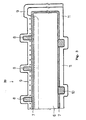
- a solar cell 10 constructed according to the invention, which consists of a p-doped silicon substrate as the body 1, a thin silicon oxide layer 2, ohmic contacts 4 arranged directly on the silicon body 1 and an MIS (metal -Insulator-Semiconductor) Contact, which in turn is composed of the p-silicon of the silicon body 1, the silicon oxide layer 2 and a metallization 3, preferably made of aluminum or magnesium.
- MIS metal -Insulator-Semiconductor
- the holes diffuse to the front and leave the silicon via the ohmic contacts 4.
- An electrical current front + pole, rear - pole of the solar cell 10, (in contrast to the solar cell 20 (FIG. 3) Solar cell 30 (Fig. 4)). Since the silicon azide layer 2 of the MIS contact acts as a tunnel insulator for the minority charge carriers, a thickness of 3 nm should not be exceeded.
- the boundary of the space charge zone of the MIS contact is like a dot in the drawing indicated.
- the electrical field prevailing there is used to collect the minority charge carriers.
- the ohmic contacts 4 are discontinuously applied to the semiconductor substrate, so that they do not cover the entire surface.
- the ohmic contacts 4 can form a geometry that is formed by interconnected strips, rings or dots. Passivation layers now extend between the ohmic contact regions 4, which on the one hand are composed of the natural or also below 800 ° C. silicon oxide layer 2 and a further insulator layer, which on the one hand can be a passivation and on the other hand as an anti-reflection layer.
- the thickness of the upper passivation layer 5, referred to as the first, can be approximately 80 nm and preferably consists of aluminum oxide or silicon nitride.
- the further insulator layer which is referred to as the second passivation layer, in the form of the silicon oxide layer 2, can be constructed differently on the front and rear sides of the silicon substrate 1.
- the thickness on the front can be varied within a wide range since it does not act as a tunnel insulator.
- the layer 2 can also be omitted completely, that is to say also in the region of the first passivation layer 3 —as also in the case of the exemplary embodiments in FIGS. 3 and 4-.
- a natural silicon oxide layer is understood to be that which is always present on the silicon substrate 1 and is only a few atomic layers thick.
- the silicon oxide layer 2 itself can be changed in its structural composition on the front side by the subsequent deposition of the first passivation layer 5-eg silicon nitride.
- silicon oxide can be converted into silicon oxynitride.
- the charge carriers that are mainly generated by the light near the front first have to diffuse through the entire substrate 1 in order to be collected by the MIS contact on the rear. It is important that the front side has a low surface recombination speed, since otherwise a large part of the charge carriers would already recombine there.
- the distance between the ohmic contact areas 4 characterized by very high recombination, which are also referred to as contact fingers, should be substantially greater than the substrate thickness d or the diffusion length of the minority charge carriers, so that on average the path to the collecting MIS contact is less than to the ohmic contact area.
- the distance between the ohmic contact fingers 4 is limited at the top by the series resistance, which is increased by insufficient ohmic contact areas to the silicon body 1.
- the optimal distance is in the range of 1 to 5 mm, the finger width in the range of 50 - 300 ⁇ m, which means that a contact area percentage of less than 10% can be achieved.
- the cell 10 has a higher collection efficiency, the thinner the semiconductor substrate and the greater its diffusion length L (d ⁇ L).
- the maximum efficiency is obtained with a thickness d of the silicon substrate 1 of approximately 50-80 ⁇ m. Therefore, expensive semiconductor material can be saved, which leads to a considerable reduction in the cost of the solar cell.
- the rear metal 3 serves as a reflector for the large wavelengths of light, which leads to an increase in the short-circuit current and to less heating during operation of the cell (higher open circuit voltage). Furthermore, the entire cell cross-section is used for the current flow, the minority charge carriers do not have to be in a narrow area of high sheet resistance (eg n+ emitter area be n+p solar cell) along the surface flow to the contacts. A high fill factor is therefore also pre-programmed. The solar cell 10 is therefore also particularly suitable for concentrated sunlight.
- FIG. 3 and 4 show further configurations of solar cells 20 and 30 which obey the teaching according to the invention.
- the respective ohmic contact is arranged on the back of the solar cell 20 or 30, and also in certain areas, as already explained in connection with FIG. 2.
- the solar cell 20 shown in FIG. 3 corresponds to the basic structure according to the silicon nitride inversion layer solar cell with MIS contact described in DE-PS 28 40 096.
- a thin silicon oxide layer 7 is located on a silicon substrate or body 6, which corresponds in particular in the area of the MIS contacts to the oxide layer 2 on the rear side of the solar cell structure shown in FIG. 2.
- the thickness of the oxide layer 7 can be varied within wide limits; the statements made there for the oxide layer 2 on the front side of the solar cell structure 10 shown in FIG. 2 apply.
- the metals 8, preferably in the form of aluminum or magnesium, of the MIS contacts are preferably arranged in strip form on the front side of the solar cell 20.
- a further insulator layer 9, which preferably consists of silicon nitride, extends over the entire surface of the solar cell. In this silicon nitride layer 9 there must be a high density of positive charges consisting of the natural charges and those introduced by foreign ions, which induce an inversion layer consisting of electrons on the surface of the p-doped silicon substrate 6. In contrast to the solar cell 10 (FIG.
- the passivation of the area between the ohmic contacts 10 prevents the electrons from recombining with the holes there, in particular when the light is incident from the rear, and thus being lost.
- the high density of positive charge is indicated in layer 9 by plus signs, the inversion layer by the dashed line.
- the dash-dotted line also indicates the width of the space charge zone.
- the silicon nitride layer 9 can only be deposited or at low temperatures ( ⁇ 300 ° C.) be annealed, otherwise the MIS contacts would be severely impaired.
- the back of the solar cell of FIG. 3 consists of strip-shaped ohmic contacts 10 (preferably A1) and the between them and in Edge region lying double insulator layer, which is formed from the thin silicon oxide layer 7 and the insulator layer 11, preferably made of Al oxide or Si nitride.
- This rear side arrangement which is the focus of the present exemplary embodiments, corresponds to the front side of the solar cell 10 shown in FIG. 2, in particular reference should be made to the comments made there with respect to the oxide layer 2 (corresponds to layer 7 in FIG. 3).
- the rear side passivation in combination with the ohmic contact region 10 represents a process which is fully compatible with this low-temperature cell type (MIS inversion view solar cell), since a temperature treatment between 400 ° C. and 600 ° C., as occurs during the deposition or tempering of the rear side insulator layer 11 is used, is anyway necessary to produce the tunnel oxide layer 7 on the front and to form the ohmic contacts 10. These processes naturally take place before the MIS contacts 8 are formed and the antireflection layer 9 is deposited on the front side.
- This cell type is particularly suitable for thin substrates 6, in which edge passivation to prevent a short circuit between the front and rear is usually a problem. This is automatically solved here by applying the passivation layers, i.e. the insulator layers.
- a potential barrier is formed in the semiconductor on the top of the cell in the edge region by overlapping the two insulator layers 9 and 11, which prevents the charge carriers from flowing off on the semiconductor surface in the edge region to the rear.
- This potential barrier arises from the fact that there is a high positive charge density in the front-side insulator 9 and a negative or at least a greatly reduced positive charge density in the rear and edge-side insulator film 11.
- the entire solar cell 20 is enveloped by the impermeable insulator layers 9 and 11, and thus protected from external influences.
- the cell 20 now uses the radiation hitting both surfaces very effectively, that is to say also the radiation hitting the rear, reflected or scattered on white surfaces.
- the insulator layer 11 on the back therefore also serves as an anti-reflection layer.
- the power output by the cell 20 can be increased considerably.
- a simple type of cell which can be produced at low temperatures and with which the sunlight can be utilized much more was thus created with almost no additional cost for expensive semiconductor material 6.
- the short-term light is used well because of the higher quality of the back.
- the light striking the rear is converted into electricity with an efficiency that is reduced by only about 10% compared to the front lighting. If the radiation from behind is not to be used, then a rear reflector can be produced simply by applying a metal layer to the rear insulator 11.
- the front and back can be textured to increase the incidence of light.
- n+p solar cell 30 which obeys the teaching according to the invention will be described, which can be a conventional n+p or p+n solar cell.
- the n+p solar cell 30 shown in the exemplary embodiment comprises a semiconductor substrate 12, a highly doped surface layer 13 (here n+), on the front a non-planar ohmic contact 14 in the form of a grid and a front-side anti-reflection layer 15
- the rear side also contains ohmic contacts 16, which are not arranged in a planar manner, preferably lattice-shaped, and the passivation layers which characterize the present invention are preferably located in Form of a silicon oxide layer 17 and an insulating layer 18 which also acts as an anti-reflection layer.
- the insulating layer 18 is preferably formed from aluminum oxide or silicon nitride. Due to the rear design according to the invention of the nconp solar cell 30, a solar cell which can be illuminated on both sides is provided in a simple manner with the additional advantage that the long-wave heat radiation emerges from the cell 30 and thus the operating temperature (increase in the open circuit voltage) drops. Furthermore, texturing, particularly of the back, is easily possible. In addition to the edge passivation by the layers 17 and 18, a complete covering of the cell 30 with impermeable insulator layers 18 and 15 can be achieved as protection. Furthermore, a metal layer can be applied to the insulator layer 18 as a rear side reflector.
- This solar cell 30 differs from the MIS inversion layer solar cell 20 (FIG. 3) in that a high-temperature process in the silicon body 12 introduces a surface layer highly doped with foreign atoms (for example phosphorus), which means that between the layers 12 and 13 an n+p transition and thus an electric field is generated. As a result of the electric field, the electrons generated by the light migrate to the surface, where they reach the ohmic contacts 14 in an external circuit along the highly conductive n + layer 13. The holes migrate to the rear and leave the silicon body 12 via the ohmic contacts 16 (front - pole, rear + pole of the solar cell 30).
- a high-temperature process in the silicon body 12 introduces a surface layer highly doped with foreign atoms (for example phosphorus), which means that between the layers 12 and 13 an n+p transition and thus an electric field is generated.
- the electrons generated by the light migrate to the surface, where they reach the ohmic contacts 14 in an external circuit along the highly conductive n +
- the silicon body consists practically of two parts 12 and 13
- the solar cells 10 (FIG. 2) and 20 (FIG. 3) are homogeneous silicon bodies 1 and 6, respectively, which are produced by the manufacturing process Cell cannot be changed.
Landscapes
- Photovoltaic Devices (AREA)
- Electromechanical Clocks (AREA)
Priority Applications (1)
| Application Number | Priority Date | Filing Date | Title |
|---|---|---|---|
| AT86113926T ATE64240T1 (de) | 1985-10-11 | 1986-10-08 | Solarzelle. |
Applications Claiming Priority (2)
| Application Number | Priority Date | Filing Date | Title |
|---|---|---|---|
| DE3536299 | 1985-10-11 | ||
| DE19853536299 DE3536299A1 (de) | 1985-10-11 | 1985-10-11 | Solarzelle aus silizium |
Publications (2)
| Publication Number | Publication Date |
|---|---|
| EP0219763A1 true EP0219763A1 (fr) | 1987-04-29 |
| EP0219763B1 EP0219763B1 (fr) | 1991-06-05 |
Family
ID=6283352
Family Applications (1)
| Application Number | Title | Priority Date | Filing Date |
|---|---|---|---|
| EP86113926A Expired - Lifetime EP0219763B1 (fr) | 1985-10-11 | 1986-10-08 | Cellule solaire |
Country Status (18)
| Country | Link |
|---|---|
| US (2) | US4828628A (fr) |
| EP (1) | EP0219763B1 (fr) |
| JP (1) | JPS63501668A (fr) |
| KR (1) | KR940010161B1 (fr) |
| AT (1) | ATE64240T1 (fr) |
| AU (1) | AU590803B2 (fr) |
| BR (1) | BR8606917A (fr) |
| DE (3) | DE3536299A1 (fr) |
| DZ (1) | DZ996A1 (fr) |
| EG (1) | EG17560A (fr) |
| ES (1) | ES2023360B3 (fr) |
| GR (1) | GR3002657T3 (fr) |
| IL (1) | IL80278A0 (fr) |
| IN (1) | IN164598B (fr) |
| MA (1) | MA20789A1 (fr) |
| MX (1) | MX171858B (fr) |
| TN (1) | TNSN86141A1 (fr) |
| WO (1) | WO1987002513A1 (fr) |
Cited By (3)
| Publication number | Priority date | Publication date | Assignee | Title |
|---|---|---|---|---|
| EP0286917A3 (en) * | 1987-04-13 | 1990-01-17 | Nukem Gmbh | Solar cell |
| EP0301471A3 (en) * | 1987-07-30 | 1990-01-31 | Nukem Gmbh | Process to reutilize a silicon base material of a metal-insulator-semiconductor (mis) inversion layer solar cell |
| DE19729522A1 (de) * | 1997-07-10 | 1999-01-28 | Dirk Dipl Ing Koenig | Anordnung zum Aufbau einer Solarzelle für polykristalline lamorphe Halbleiter |
Families Citing this family (46)
| Publication number | Priority date | Publication date | Assignee | Title |
|---|---|---|---|---|
| US5215599A (en) * | 1991-05-03 | 1993-06-01 | Electric Power Research Institute | Advanced solar cell |
| US5320684A (en) * | 1992-05-27 | 1994-06-14 | Mobil Solar Energy Corporation | Solar cell and method of making same |
| KR100416741B1 (ko) * | 1997-03-31 | 2004-05-17 | 삼성전자주식회사 | 후면 부분소결형 실리콘 태양전지 |
| GB2325081B (en) * | 1997-05-06 | 2000-01-26 | Simage Oy | Semiconductor imaging device |
| US20060021648A1 (en) * | 1997-05-09 | 2006-02-02 | Parise Ronald J | Device and method to transmit waste heat or thermal pollution into deep space |
| US5936193A (en) * | 1997-05-09 | 1999-08-10 | Parise; Ronald J. | Nighttime solar cell |
| JPH11103079A (ja) * | 1997-09-26 | 1999-04-13 | Sanyo Electric Co Ltd | 集積型光起電力装置の製造方法 |
| US6774300B2 (en) * | 2001-04-27 | 2004-08-10 | Adrena, Inc. | Apparatus and method for photovoltaic energy production based on internal charge emission in a solid-state heterostructure |
| US7659475B2 (en) * | 2003-06-20 | 2010-02-09 | Imec | Method for backside surface passivation of solar cells and solar cells with such passivation |
| JP4232597B2 (ja) * | 2003-10-10 | 2009-03-04 | 株式会社日立製作所 | シリコン太陽電池セルとその製造方法 |
| US20060060238A1 (en) * | 2004-02-05 | 2006-03-23 | Advent Solar, Inc. | Process and fabrication methods for emitter wrap through back contact solar cells |
| DE102005026176B3 (de) * | 2005-06-06 | 2007-01-04 | Universität Konstanz | Verfahren zur flächigen Kontaktierung von Halbleiterbauelementen mit reduzierter Durchbiegung sowie entsprechendes Halbleiterbauelement und Herstellungsvorrichtung |
| JP4837662B2 (ja) * | 2005-06-22 | 2011-12-14 | 京セラ株式会社 | 太陽電池素子の製造方法 |
| CN101305472B (zh) * | 2005-11-08 | 2011-07-13 | Lg电子株式会社 | 高效太阳能电池及其制备方法 |
| US20100032012A1 (en) * | 2006-12-01 | 2010-02-11 | Takayuki Isaka | Solar cell and method of manufacturing the same |
| KR100974220B1 (ko) * | 2006-12-13 | 2010-08-06 | 엘지전자 주식회사 | 태양전지 |
| JP5219538B2 (ja) * | 2008-02-12 | 2013-06-26 | 大成建設株式会社 | 太陽光発電薄膜を基材に直接形成した太陽電池 |
| KR100953448B1 (ko) * | 2008-04-02 | 2010-04-20 | 한국기계연구원 | 반도체 나노소재를 이용한 광전 변환 장치 및 그 제조 방법 |
| US20090260685A1 (en) * | 2008-04-17 | 2009-10-22 | Daeyong Lee | Solar cell and method of manufacturing the same |
| CN102099923B (zh) * | 2008-06-11 | 2016-04-27 | 因特瓦克公司 | 使用注入的太阳能电池制作 |
| SG174289A1 (en) * | 2009-03-20 | 2011-10-28 | Solar Implant Technologies Inc | Advanced high efficiency crystalline solar cell fabrication method |
| JP5334645B2 (ja) * | 2009-03-31 | 2013-11-06 | 富士フイルム株式会社 | 可撓性太陽電池モジュール |
| JP2010283339A (ja) * | 2009-05-02 | 2010-12-16 | Semiconductor Energy Lab Co Ltd | 光電変換装置及びその作製方法 |
| DE102009024807B3 (de) | 2009-06-02 | 2010-10-07 | Helmholtz-Zentrum Berlin Für Materialien Und Energie Gmbh | Solarzelle mit benachbarten elektrisch isolierenden Passivierbereichen mit hoher Oberflächenladung gegensätzlicher Polarität und Herstellungsverfahren |
| KR101139458B1 (ko) * | 2009-06-18 | 2012-04-30 | 엘지전자 주식회사 | 태양전지 및 그 제조방법 |
| KR101032624B1 (ko) | 2009-06-22 | 2011-05-06 | 엘지전자 주식회사 | 태양 전지 및 그 제조 방법 |
| US8749053B2 (en) | 2009-06-23 | 2014-06-10 | Intevac, Inc. | Plasma grid implant system for use in solar cell fabrications |
| US20110041910A1 (en) * | 2009-08-18 | 2011-02-24 | Semiconductor Energy Laboratory Co., Ltd. | Photoelectric conversion device and manufacturing method thereof |
| TWI497730B (zh) * | 2009-10-20 | 2015-08-21 | Iner Aec Executive Yuan | 一種薄膜光伏裝置及其製造方法 |
| KR20110062598A (ko) * | 2009-12-03 | 2011-06-10 | 삼성전자주식회사 | 적층막 제조방법, 이를 이용한 태양전지의 제조방법 |
| TW201123480A (en) * | 2009-12-29 | 2011-07-01 | Auria Solar Co Ltd | Solar cell structure and manufacturing method thereof |
| US20110272024A1 (en) * | 2010-04-13 | 2011-11-10 | Applied Materials, Inc. | MULTI-LAYER SiN FOR FUNCTIONAL AND OPTICAL GRADED ARC LAYERS ON CRYSTALLINE SOLAR CELLS |
| US8686283B2 (en) | 2010-05-04 | 2014-04-01 | Silevo, Inc. | Solar cell with oxide tunneling junctions |
| KR101203623B1 (ko) * | 2010-06-18 | 2012-11-21 | 엘지전자 주식회사 | 태양 전지 및 그 제조 방법 |
| US20120060918A1 (en) * | 2010-08-16 | 2012-03-15 | Spitzer Mark B | Energy conversion device for photovoltaic cells |
| US20120048376A1 (en) * | 2010-08-30 | 2012-03-01 | Alexander Shkolnik | Silicon-based photovoltaic device produced by essentially electrical means |
| US20120073650A1 (en) * | 2010-09-24 | 2012-03-29 | David Smith | Method of fabricating an emitter region of a solar cell |
| KR101258938B1 (ko) | 2011-07-25 | 2013-05-07 | 엘지전자 주식회사 | 태양 전지 |
| KR20140110851A (ko) | 2011-11-08 | 2014-09-17 | 인테벡, 인코포레이티드 | 기판 프로세싱 시스템 및 방법 |
| WO2014092677A1 (fr) * | 2012-12-10 | 2014-06-19 | Alliance For Sustainable Engery, Llc | Cellules solaires à jonctions multiples monolithiques à tension adaptée en tandem |
| TWI570745B (zh) | 2012-12-19 | 2017-02-11 | 因特瓦克公司 | 用於電漿離子植入之柵極 |
| DE112013005591C5 (de) | 2013-06-26 | 2018-10-04 | Universität Konstanz | Verfahren und Vorrichtung zum Herstellen eines Photovoltaikelements mit stabilisiertem Wirkungsgrad |
| US9466755B2 (en) * | 2014-10-30 | 2016-10-11 | International Business Machines Corporation | MIS-IL silicon solar cell with passivation layer to induce surface inversion |
| JP2017033970A (ja) * | 2015-07-29 | 2017-02-09 | 京セラ株式会社 | 太陽電池素子およびその製造方法 |
| CN117497633B (zh) | 2023-04-12 | 2024-06-04 | 天合光能股份有限公司 | 薄膜制备方法、太阳能电池、光伏组件和光伏系统 |
| CN220543924U (zh) * | 2023-06-25 | 2024-02-27 | 天合光能股份有限公司 | 太阳能电池、光伏组件和光伏系统 |
Citations (5)
| Publication number | Priority date | Publication date | Assignee | Title |
|---|---|---|---|---|
| DE1614832A1 (de) * | 1967-06-27 | 1970-12-23 | Telefunken Patent | Doppelsperrschichtsolarzelle |
| FR2303384A1 (fr) * | 1975-03-07 | 1976-10-01 | Rca Corp | Dispositif a cellule solaire a rendement ameliore |
| DE2846097A1 (de) * | 1978-10-23 | 1980-04-24 | Rudolf Dipl Phys Dr Hezel | Solarzelle mit verbessertem wirkungsgrad aus einer halbleiteranordnung |
| GB2034973A (en) * | 1978-10-23 | 1980-06-11 | Hezel R | Solar cell with multi-layer insulation |
| EP0118797A2 (fr) * | 1983-03-09 | 1984-09-19 | Licentia Patent-Verwaltungs-GmbH | Cellule solaire |
Family Cites Families (14)
| Publication number | Priority date | Publication date | Assignee | Title |
|---|---|---|---|---|
| US4064521A (en) * | 1975-07-28 | 1977-12-20 | Rca Corporation | Semiconductor device having a body of amorphous silicon |
| JPS5329588A (en) * | 1976-08-31 | 1978-03-18 | Shin Meiwa Ind Co Ltd | Apparatus for holding and withdrawing wires in equipment for continuously compressing terminals of a plurality of wires |
| DE2853412A1 (de) * | 1978-12-11 | 1980-07-03 | Rudolf Dr Hezel | Solarzelle aus halbleitermaterial |
| DE2846096C2 (de) * | 1978-10-23 | 1985-01-10 | Rudolf Dipl.-Phys. Dr. 8521 Spardorf Hezel | Solarzelle aus Halbleitermaterial |
| JPS5766677A (en) * | 1980-10-09 | 1982-04-22 | Toshiba Corp | Solar battery cell and manufacture thereof |
| US4315097A (en) * | 1980-10-27 | 1982-02-09 | Mcdonnell Douglas Corporation | Back contacted MIS photovoltaic cell |
| JPS57178380A (en) * | 1981-04-27 | 1982-11-02 | Semiconductor Energy Lab Co Ltd | Manufacture of mis type photoelectric transducer |
| JPS5839074A (ja) * | 1981-08-31 | 1983-03-07 | Mitsubishi Electric Corp | 太陽電池の製造方法 |
| JPS58128775A (ja) * | 1982-01-28 | 1983-08-01 | Toshiba Corp | 太陽電池の製造方法 |
| CA1209681A (fr) * | 1982-08-04 | 1986-08-12 | Exxon Research And Engineering Company | Dispositif photovoltaique a couche mince utilisant des surfaces a structure aleatoire obtenues par lithographie |
| AU566712B2 (en) * | 1983-10-20 | 1987-10-29 | Unisearch Limited | High efficiency solar cells |
| US4525593A (en) * | 1984-04-16 | 1985-06-25 | Exxon Research And Engineering Co. | Inverted, optically enhanced solar cell |
| DE3420887A1 (de) * | 1984-06-05 | 1985-12-05 | Telefunken electronic GmbH, 7100 Heilbronn | Solarzelle |
| US4667060A (en) * | 1985-05-28 | 1987-05-19 | Spire Corporation | Back junction photovoltaic solar cell |
-
1985
- 1985-10-11 DE DE19853536299 patent/DE3536299A1/de not_active Withdrawn
-
1986
- 1986-10-08 JP JP61505390A patent/JPS63501668A/ja active Pending
- 1986-10-08 DE DE86EP8600573T patent/DE3690520D2/de not_active Expired
- 1986-10-08 BR BR8606917A patent/BR8606917A/pt not_active IP Right Cessation
- 1986-10-08 US US07/059,264 patent/US4828628A/en not_active Expired - Fee Related
- 1986-10-08 DZ DZ860210A patent/DZ996A1/fr active
- 1986-10-08 AT AT86113926T patent/ATE64240T1/de not_active IP Right Cessation
- 1986-10-08 KR KR1019870700498A patent/KR940010161B1/ko not_active Expired - Fee Related
- 1986-10-08 WO PCT/EP1986/000573 patent/WO1987002513A1/fr not_active Ceased
- 1986-10-08 ES ES86113926T patent/ES2023360B3/es not_active Expired - Lifetime
- 1986-10-08 DE DE8686113926T patent/DE3679629D1/de not_active Expired - Fee Related
- 1986-10-08 EP EP86113926A patent/EP0219763B1/fr not_active Expired - Lifetime
- 1986-10-08 AU AU64758/86A patent/AU590803B2/en not_active Ceased
- 1986-10-09 EG EG632/86A patent/EG17560A/xx active
- 1986-10-09 MX MX003987A patent/MX171858B/es unknown
- 1986-10-09 IN IN736/CAL/86A patent/IN164598B/en unknown
- 1986-10-10 MA MA21019A patent/MA20789A1/fr unknown
- 1986-10-10 IL IL80278A patent/IL80278A0/xx not_active IP Right Cessation
- 1986-10-13 TN TNTNSN86141A patent/TNSN86141A1/fr unknown
-
1988
- 1988-12-14 US US07/284,420 patent/US4900369A/en not_active Expired - Fee Related
-
1991
- 1991-09-05 GR GR91401265T patent/GR3002657T3/el unknown
Patent Citations (5)
| Publication number | Priority date | Publication date | Assignee | Title |
|---|---|---|---|---|
| DE1614832A1 (de) * | 1967-06-27 | 1970-12-23 | Telefunken Patent | Doppelsperrschichtsolarzelle |
| FR2303384A1 (fr) * | 1975-03-07 | 1976-10-01 | Rca Corp | Dispositif a cellule solaire a rendement ameliore |
| DE2846097A1 (de) * | 1978-10-23 | 1980-04-24 | Rudolf Dipl Phys Dr Hezel | Solarzelle mit verbessertem wirkungsgrad aus einer halbleiteranordnung |
| GB2034973A (en) * | 1978-10-23 | 1980-06-11 | Hezel R | Solar cell with multi-layer insulation |
| EP0118797A2 (fr) * | 1983-03-09 | 1984-09-19 | Licentia Patent-Verwaltungs-GmbH | Cellule solaire |
Non-Patent Citations (2)
| Title |
|---|
| APPLIED PHYSICS LETTERS, Band 39, Nr. 1, 1. July 1981, Seiten 83-85, American Institute of Physics, New York, US; N.G. TARR et al.: "Induced back-surface field solar cells on p-type silicon substrates" * |
| PATENTS ABSTRACTS OF JAPAN, Band 9, Nr. 140 (E-321)[1863], 14. Juni 1985; & JP-A-60 22 380 (NIPPON DENSHIN DENWA KOSHA) 04.02.1985 * |
Cited By (4)
| Publication number | Priority date | Publication date | Assignee | Title |
|---|---|---|---|---|
| EP0286917A3 (en) * | 1987-04-13 | 1990-01-17 | Nukem Gmbh | Solar cell |
| EP0301471A3 (en) * | 1987-07-30 | 1990-01-31 | Nukem Gmbh | Process to reutilize a silicon base material of a metal-insulator-semiconductor (mis) inversion layer solar cell |
| DE19729522A1 (de) * | 1997-07-10 | 1999-01-28 | Dirk Dipl Ing Koenig | Anordnung zum Aufbau einer Solarzelle für polykristalline lamorphe Halbleiter |
| DE19729522C2 (de) * | 1997-07-10 | 2001-11-08 | Dirk Koenig | Anordnung zum Aufbau einer Solarzelle für polykristalline oder amorphe Halbleiter |
Also Published As
| Publication number | Publication date |
|---|---|
| IN164598B (fr) | 1989-04-15 |
| KR880700475A (ko) | 1988-03-15 |
| ES2023360B3 (es) | 1992-01-16 |
| DZ996A1 (fr) | 2004-09-13 |
| MA20789A1 (fr) | 1987-07-01 |
| IL80278A0 (en) | 1987-01-30 |
| KR940010161B1 (ko) | 1994-10-22 |
| US4828628A (en) | 1989-05-09 |
| JPS63501668A (ja) | 1988-06-23 |
| US4900369A (en) | 1990-02-13 |
| BR8606917A (pt) | 1987-11-03 |
| WO1987002513A1 (fr) | 1987-04-23 |
| DE3536299A1 (de) | 1987-04-16 |
| EP0219763B1 (fr) | 1991-06-05 |
| EG17560A (en) | 1990-10-30 |
| TNSN86141A1 (fr) | 1990-01-01 |
| ATE64240T1 (de) | 1991-06-15 |
| GR3002657T3 (en) | 1993-01-25 |
| MX171858B (es) | 1993-11-22 |
| DE3679629D1 (de) | 1991-07-11 |
| DE3690520D2 (en) | 1987-11-19 |
| AU6475886A (en) | 1987-05-05 |
| AU590803B2 (en) | 1989-11-16 |
Similar Documents
| Publication | Publication Date | Title |
|---|---|---|
| EP0219763B1 (fr) | Cellule solaire | |
| EP3930013B1 (fr) | Procédé de fabrication d'une cellule solaire photovoltaïque dotée d'au moins une hétérojonction | |
| DE202023101112U1 (de) | Solarzelle und Photovoltaikmodul | |
| EP1875517B1 (fr) | Cellule solaire a heterocontact presentant une geometrie inversee de structure de couches | |
| DE10237515A1 (de) | Stapelförmiger photoelektrischer Wandler | |
| DE102020132245A1 (de) | Rückseitenkontaktierte Solarzelle und Herstellung einer solchen | |
| EP0286917A2 (fr) | Cellule solaire | |
| DE3732619C2 (fr) | ||
| DE212013000122U1 (de) | Hybrid-Solarzelle | |
| DE2846096C2 (de) | Solarzelle aus Halbleitermaterial | |
| WO2024008455A1 (fr) | Cellule solaire à contact arrière comprenant des contacts passivés, et procédé de fabrication | |
| DE202025004152U1 (de) | Solarzelle, Photovoltaikmodul | |
| EP2671264B1 (fr) | Cellule solaire photovoltaïque et son procédé de fabrication | |
| DE202025004140U1 (de) | Solarzelle und Photovoltaikmodul | |
| DE102011115581B4 (de) | Verfahren zur Herstellung einer Solarzelle | |
| DE102009043975A1 (de) | Solarzelle | |
| EP2534697B1 (fr) | Cellule solaire à contact arrière comportant une couche absorbante non structurée | |
| DE102010020557A1 (de) | Verfahren zur Herstellung einer einseitig kontaktierbaren Solarzelle aus einem Silizium-Halbleitersubstrat | |
| DE102013219565A1 (de) | Photovoltaische Solarzelle und Verfahren zum Herstellen einer photovoltaischen Solarzelle | |
| EP2327102A1 (fr) | Procédé pour la mise en contact locale et le dopage local d'une couche semi-conductrice | |
| DE4143083A1 (de) | Solarzelle | |
| DE102016110965B4 (de) | Halbleiter-Bauelement mit vorder- und rückseitiger Elektrode und Verfahren zu dessen Herstellung | |
| EP4147277B1 (fr) | Cellule solaire mise en contact du côté arrière | |
| DE112025000104T5 (de) | Rückseitenkontaktierte solarzelle, photovoltaikmodul und photovoltaiksystem | |
| WO2024104976A1 (fr) | Cellule solaire ayant une structure de contact avant qui comprend une couche de carbure de silicium, et procédé de fabrication de ladite cellule solaire |
Legal Events
| Date | Code | Title | Description |
|---|---|---|---|
| PUAI | Public reference made under article 153(3) epc to a published international application that has entered the european phase |
Free format text: ORIGINAL CODE: 0009012 |
|
| AK | Designated contracting states |
Kind code of ref document: A1 Designated state(s): AT BE CH DE ES FR GB GR IT LI LU NL SE |
|
| RIN1 | Information on inventor provided before grant (corrected) |
Inventor name: HACKSTEIN,KARL GERHARD,DR.DIPL.-CHEM. Inventor name: HEZEL, RUDOLF, DR. DIPL.-PHYS. |
|
| 17P | Request for examination filed |
Effective date: 19870811 |
|
| 17Q | First examination report despatched |
Effective date: 19880630 |
|
| GRAA | (expected) grant |
Free format text: ORIGINAL CODE: 0009210 |
|
| RAP1 | Party data changed (applicant data changed or rights of an application transferred) |
Owner name: NUKEM GMBH |
|
| AK | Designated contracting states |
Kind code of ref document: B1 Designated state(s): AT BE CH DE ES FR GB GR IT LI LU NL SE |
|
| REF | Corresponds to: |
Ref document number: 64240 Country of ref document: AT Date of ref document: 19910615 Kind code of ref document: T |
|
| REF | Corresponds to: |
Ref document number: 3679629 Country of ref document: DE Date of ref document: 19910711 |
|
| ITF | It: translation for a ep patent filed | ||
| ET | Fr: translation filed | ||
| GBT | Gb: translation of ep patent filed (gb section 77(6)(a)/1977) | ||
| REG | Reference to a national code |
Ref country code: ES Ref legal event code: FG2A Ref document number: 2023360 Country of ref document: ES Kind code of ref document: B3 |
|
| PLBE | No opposition filed within time limit |
Free format text: ORIGINAL CODE: 0009261 |
|
| STAA | Information on the status of an ep patent application or granted ep patent |
Free format text: STATUS: NO OPPOSITION FILED WITHIN TIME LIMIT |
|
| 26N | No opposition filed | ||
| REG | Reference to a national code |
Ref country code: GR Ref legal event code: FG4A Free format text: 3002657 |
|
| EPTA | Lu: last paid annual fee | ||
| PGFP | Annual fee paid to national office [announced via postgrant information from national office to epo] |
Ref country code: LU Payment date: 19941001 Year of fee payment: 9 |
|
| PGFP | Annual fee paid to national office [announced via postgrant information from national office to epo] |
Ref country code: GR Payment date: 19941019 Year of fee payment: 9 |
|
| PGFP | Annual fee paid to national office [announced via postgrant information from national office to epo] |
Ref country code: SE Payment date: 19941020 Year of fee payment: 9 |
|
| PGFP | Annual fee paid to national office [announced via postgrant information from national office to epo] |
Ref country code: CH Payment date: 19941024 Year of fee payment: 9 |
|
| EAL | Se: european patent in force in sweden |
Ref document number: 86113926.9 |
|
| PG25 | Lapsed in a contracting state [announced via postgrant information from national office to epo] |
Ref country code: LU Free format text: LAPSE BECAUSE OF NON-PAYMENT OF DUE FEES Effective date: 19951008 |
|
| PG25 | Lapsed in a contracting state [announced via postgrant information from national office to epo] |
Ref country code: SE Effective date: 19951009 |
|
| PG25 | Lapsed in a contracting state [announced via postgrant information from national office to epo] |
Ref country code: LI Effective date: 19951031 Ref country code: CH Effective date: 19951031 |
|
| PG25 | Lapsed in a contracting state [announced via postgrant information from national office to epo] |
Ref country code: GR Free format text: THE PATENT HAS BEEN ANNULLED BY A DECISION OF A NATIONAL AUTHORITY Effective date: 19960430 |
|
| REG | Reference to a national code |
Ref country code: CH Ref legal event code: PL |
|
| REG | Reference to a national code |
Ref country code: GR Ref legal event code: MM2A Free format text: 3002657 |
|
| EUG | Se: european patent has lapsed |
Ref document number: 86113926.9 |
|
| PGFP | Annual fee paid to national office [announced via postgrant information from national office to epo] |
Ref country code: GB Payment date: 19961004 Year of fee payment: 11 |
|
| PGFP | Annual fee paid to national office [announced via postgrant information from national office to epo] |
Ref country code: AT Payment date: 19961030 Year of fee payment: 11 |
|
| PGFP | Annual fee paid to national office [announced via postgrant information from national office to epo] |
Ref country code: BE Payment date: 19961031 Year of fee payment: 11 |
|
| PG25 | Lapsed in a contracting state [announced via postgrant information from national office to epo] |
Ref country code: GB Free format text: LAPSE BECAUSE OF NON-PAYMENT OF DUE FEES Effective date: 19971008 Ref country code: AT Free format text: LAPSE BECAUSE OF NON-PAYMENT OF DUE FEES Effective date: 19971008 |
|
| PGFP | Annual fee paid to national office [announced via postgrant information from national office to epo] |
Ref country code: ES Payment date: 19971016 Year of fee payment: 12 |
|
| PGFP | Annual fee paid to national office [announced via postgrant information from national office to epo] |
Ref country code: FR Payment date: 19971020 Year of fee payment: 12 |
|
| PGFP | Annual fee paid to national office [announced via postgrant information from national office to epo] |
Ref country code: DE Payment date: 19971030 Year of fee payment: 12 |
|
| PG25 | Lapsed in a contracting state [announced via postgrant information from national office to epo] |
Ref country code: BE Free format text: LAPSE BECAUSE OF NON-PAYMENT OF DUE FEES Effective date: 19971031 |
|
| PGFP | Annual fee paid to national office [announced via postgrant information from national office to epo] |
Ref country code: NL Payment date: 19971031 Year of fee payment: 12 |
|
| BERE | Be: lapsed |
Owner name: NUKEM G.M.B.H. Effective date: 19971031 |
|
| GBPC | Gb: european patent ceased through non-payment of renewal fee |
Effective date: 19971008 |
|
| PG25 | Lapsed in a contracting state [announced via postgrant information from national office to epo] |
Ref country code: ES Free format text: THE PATENT HAS BEEN ANNULLED BY A DECISION OF A NATIONAL AUTHORITY Effective date: 19981009 |
|
| PG25 | Lapsed in a contracting state [announced via postgrant information from national office to epo] |
Ref country code: NL Free format text: LAPSE BECAUSE OF NON-PAYMENT OF DUE FEES Effective date: 19990501 |
|
| PG25 | Lapsed in a contracting state [announced via postgrant information from national office to epo] |
Ref country code: FR Free format text: LAPSE BECAUSE OF NON-PAYMENT OF DUE FEES Effective date: 19990630 |
|
| NLV4 | Nl: lapsed or anulled due to non-payment of the annual fee |
Effective date: 19990501 |
|
| REG | Reference to a national code |
Ref country code: FR Ref legal event code: ST |
|
| PG25 | Lapsed in a contracting state [announced via postgrant information from national office to epo] |
Ref country code: DE Free format text: LAPSE BECAUSE OF NON-PAYMENT OF DUE FEES Effective date: 19990803 |
|
| REG | Reference to a national code |
Ref country code: ES Ref legal event code: FD2A Effective date: 20001204 |
|
| PG25 | Lapsed in a contracting state [announced via postgrant information from national office to epo] |
Ref country code: IT Free format text: LAPSE BECAUSE OF NON-PAYMENT OF DUE FEES;WARNING: LAPSES OF ITALIAN PATENTS WITH EFFECTIVE DATE BEFORE 2007 MAY HAVE OCCURRED AT ANY TIME BEFORE 2007. THE CORRECT EFFECTIVE DATE MAY BE DIFFERENT FROM THE ONE RECORDED. Effective date: 20051008 |