EP0220069A2 - Korrektur-/Lesegerät bezogen auf eine vorangegangene Aufzeichnung - Google Patents
Korrektur-/Lesegerät bezogen auf eine vorangegangene Aufzeichnung Download PDFInfo
- Publication number
- EP0220069A2 EP0220069A2 EP86308072A EP86308072A EP0220069A2 EP 0220069 A2 EP0220069 A2 EP 0220069A2 EP 86308072 A EP86308072 A EP 86308072A EP 86308072 A EP86308072 A EP 86308072A EP 0220069 A2 EP0220069 A2 EP 0220069A2
- Authority
- EP
- European Patent Office
- Prior art keywords
- past
- photoelectric conversion
- reading apparatus
- photosensitive elements
- level
- Prior art date
- Legal status (The legal status is an assumption and is not a legal conclusion. Google has not performed a legal analysis and makes no representation as to the accuracy of the status listed.)
- Granted
Links
- 238000006243 chemical reaction Methods 0.000 claims abstract description 42
- 238000003860 storage Methods 0.000 claims abstract description 23
- 230000003321 amplification Effects 0.000 claims description 5
- 238000003199 nucleic acid amplification method Methods 0.000 claims description 5
- 230000003287 optical effect Effects 0.000 claims description 4
- 238000010586 diagram Methods 0.000 description 13
- 230000005540 biological transmission Effects 0.000 description 10
- 238000013139 quantization Methods 0.000 description 9
- 238000000034 method Methods 0.000 description 6
- 238000005070 sampling Methods 0.000 description 6
- WUPHOULIZUERAE-UHFFFAOYSA-N 3-(oxolan-2-yl)propanoic acid Chemical compound OC(=O)CCC1CCCO1 WUPHOULIZUERAE-UHFFFAOYSA-N 0.000 description 5
- 230000008901 benefit Effects 0.000 description 5
- 229910052980 cadmium sulfide Inorganic materials 0.000 description 5
- 230000004044 response Effects 0.000 description 5
- 230000008569 process Effects 0.000 description 4
- 230000000694 effects Effects 0.000 description 3
- 230000006870 function Effects 0.000 description 3
- 230000006866 deterioration Effects 0.000 description 2
- 238000012986 modification Methods 0.000 description 2
- 230000000630 rising effect Effects 0.000 description 2
- 230000008054 signal transmission Effects 0.000 description 2
- 238000003491 array Methods 0.000 description 1
- 230000003247 decreasing effect Effects 0.000 description 1
- 230000006872 improvement Effects 0.000 description 1
- 238000004519 manufacturing process Methods 0.000 description 1
- 230000004048 modification Effects 0.000 description 1
- 230000000063 preceeding effect Effects 0.000 description 1
- 238000002360 preparation method Methods 0.000 description 1
- 230000007704 transition Effects 0.000 description 1
Images


Classifications
-
- H—ELECTRICITY
- H04—ELECTRIC COMMUNICATION TECHNIQUE
- H04N—PICTORIAL COMMUNICATION, e.g. TELEVISION
- H04N1/00—Scanning, transmission or reproduction of documents or the like, e.g. facsimile transmission; Details thereof
- H04N1/40—Picture signal circuits
- H04N1/403—Discrimination between the two tones in the picture signal of a two-tone original
Definitions
- the present invention generally relates to a reading apparatus employed in facsimile systems. More specifically, the invention relates to past record correcting/reading apparatus in which an image sensor is employed to produce photoelectric conversion outputs and the photoelectric conversion outputs are converted into signals in accordance with transmission systems.
- the reading apparatus as described in the preamble is arranged by an image sensor, an amplifier, a comparator, a lens, a light source and so on.
- an original document is illuminated by light coming from the light source, and then the light reflected from the original document is focused via the lens onto the image sensor.
- a single array, or a plurality of arrays of so-called "photosensitive elements” are arranged in a line form along a main scanning direction.
- the photosensitive elements have such characteristics that electromotive power, resistance, and charged electrons vary with the amount of light incident thereon.
- the main scanning of the image sensor is accomplished by sequentially, electronically switching the photoelectric conversion signal of the respective photosensitive elements and successively deriving them therefrom.
- the sub-scanning of the image sensor is performed by relatively transporting the origianl document, lens, or image sensor by way of mechanical means or optical means.
- the photoelectric conversion signals from the image sensor are conducted to the amplifier to be amplified.
- the amplified signals are derived from the amplifier as photoelectric conversion outputs Vs.
- the processing mode for these photoelectric conversion outputs Vs varies in accordance with the transmission systems of the facsimile signals, i.e., analog transmission systems, or digital transmission systems.
- the photoelectric conversion outputs Vs may be directly conducted to a modulator for transmission purposes, whereas in the event of digital transmission system, they may be quantized via an analog-to-digital (A/D) converter and if necessary, further be coded for transmission purposes.
- A/D analog-to-digital
- the photoelectric conversion outputs Vs are binary-quantized, based upon a reference voltage V R (slice level) of a comparator, into binary-coded signals that are derived from the output terminals as output signals of the A/D converter, assuming that photoelectric conversion outputs are indicated by Vs.
- the scanning time period ⁇ is selected to be longer than the rise time, or the fall time of the photoelectric conversion output, and the binary-quantized signal is obtained by the above-described means with maintaining substantially completely the original image information.
- the conventional reading apparatus has, however, disadvantage that resolution in the sub-scanning direction is deteriorated, an image quality is deteriorated, and a limitation is provided with the scanning speed due to the previous reasons, even if such conventional means is utilized. This is because a longer time is required when the output of the image sensor reaches the photoelectric conversion output level determined by the reflections of the original document, due to the slow photo-response characteristic of the image sensor. The deteriorations of both the resolution and image quality are emphasized particularly in the high speed scanning.
- the scanning rate is twice as the above scanning rate, i.e., the scanning time period being ⁇ /2
- the rising and falling characteristics of the photoelectric conversion output with respect to the image information are considerably deteriorated, as compared with the scanning time period of ⁇ .
- the photoelectric conversion outputs concerning small image signals do not exceed the slice level, so that the image information for the small image signals will be lost.
- the waveform of the resultant binary-coded output signal is very different from that of the original image information, resulting in serious deteriorations of the image resolution and quality.
- the present invention is made in consideration of the above-described circumstances and has therefore an object to provide a reading apparatus in which the resolution in the sub-scanning direction as well as the image quality are not harmed and the higher scanning rate can be realized even if the image sensor having slower photo-response characteristics is employed.
- a detailed object of the present invention is to provide a past record correcting/reading apparatus wherein either quantized levels or output levels of photoelectric-converted output signals derived from the respective photosensitive elements by the present scanning lines are controlled based upon the information obtained by the past scanning lines.
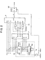
- Fig. 1 is a schematic block diagram of a past record correcting/recording apparatus according to the invention.
- the apparatus includes an image sensor 1, an amplifier 2, a lens 3, a light source 4 and an original document 5 and so on.
- the original document 5 is illuminated by the light source 4 and then, the light reflected from the document 5 is focused via the lens 3 onto the image sensor 1.
- Reference numeral 6 indicates an analog-to-digital (A/D) converter for converting the analog information from the amplifier 2 into the corresponding digital information.
- A/D analog-to-digital
- Reference numeral 7 denotes a comparator for comparing photoelectric conversion information "a" of the respective photosensitive elements of the image sensor 1, which was previously obtained during the past scanning operation and corresponds to the past scanning lines, with photoelectric conversion information "b" of the respective photosensitive elements, which is presently obtained during the present scanning operation so as to judge which information is greater than the remaining information.
- the former information is referred to as “past scanning line information”
- the later information is referred to as “present scanning line information”.
- Reference numeral 8 represents a buffer memory circuit (referred to as a “storage circuit") for storing the past scanning line information "b".
- Reference numeral 9 is a binary encoder for binary-judging the present scanning line information "a", based upon the comparision judgement output signal "c" (simply referred to as a “judgement output signal”) derived from the comparator-7 and for deriving a binary-quantized output signal (referred to as a “binary output signal”) at its output terminal "e”.
- Fig. 2 is a circuit diagram of the major circuit elements shown in F ig. 1, i.e., the comparator 7, the storage circuit 8 and the binary encoder 9.
- the scanning line information is a 4-bit input in the embodiment shown in Fig. 2.
- the light reflected from the original document 5 illumited by the light source 4 is photoelectric-converted via the lens by the image sensor 1 (for instance, a CdS (cadmium sulfide) image sensor).
- the photoelectric-converted signal is amplified in the amplifier 2 and thereafter A/D-converted in the A/D converter 6 into digital signals a o to a3 (i.e., the present scanning line information).
- the digitized present scanning line information a o to a3 is supplied to the binary encoder 9 and simultaneously to the comparator 7.
- the present scanning line information a0 to a3 is, on the other hand, written into predetermined addresses of a RAM (random access memory) 82 via a three-state buffer 81.
- the present scanning line information a to a3 written in this RA M 82 is read out as the past scanning line information b o to b 3 when the succeeding scanning line information is stored therein.
- both the writing operation of the present scanning line information a to a3 and the reading operation of the past scanning line information b o to b 3 are performed under control of an enable signal WE, as shown in the timing chart of Fig. 4. That is to say, upon input of the present scanning line information a o to a3 into the RAM 82, the past scanning line information b o to b 3 is simultaneously read out from the RAM 82 and supplied to the comparator 7.
- the comparator 7 makes a comparision between the above-described image information "a” and “b” in accordance with the preset conditions as shown in Table 1, and delivers judgement output signals C o to C 3 as comparision results to the binary encoder 9.
- values of these judgement output signals C o to C 3 vary with the comparision results between both the image information "a” and "b", and therefore determine the slice level of the binary encoder 9.
- the resultant judgement output signals (i.e., slice levels) C o to C 3 determined in the above way are used in the binary encoder 9 as the binary-quantizing levels.
- the present information a to a3 is binary-quantized and thereafter only binary image information is derived from a terminal "e" of a D type flip-flop 92 as shown in Fig. 4.
- the slice levels i.e., the judgement output signals "C" which are successively determined by comparing the magnitude of the present scanning line information "a” to that of the past scanning line information "b", are utilized as the binary-quantizing levels for the present scanning information "a".
- Figs. 5A and 5B there are shown waveforms for representing a relationship between the image information variations and the corresponding photoelectric-converted output signals which are obtained from the specific photosensitive element along the sub-scanning direction.
- Sampling points for determining the binary quantization are located at the dotted lines of the drawing.
- reference numeral 10 indicates an encoder for comparing the present scanning line information "a" with the past scanning line information "b” and for producing corrected data "f” by weight- processing the present scanning line information "a".
- the present scanning information "a” is weight-processed, or weighted by utilizing the present and past scanning line information, and then, the weighted data (corrected data "f") is binary-quantized, or binary coded by the binary-quantizing encoder 9 having the above-defined constant slice level so as to produce the binary-quantized signal for precisely producing the original image information at its output terminal "e".
- a weighting process circuit for weighting the present scanning line information "a”, as one preferred embodiment.
- the present scanning line information "a” is input in the storage circuit 8
- the past scanning line information "b” is simultaneously read from this storage circuit 8, and input into the comparator 7.
- the present scanning line information "a” is input as a minuend into an adder 101.
- the adder 101 performs the addition of +2 at its output (2).
- the subtraction result of -2 is obtained at its output ( ⁇ ).
- the corrected data "f” can be obtained from the selector 102 in accordance with the function table shown in Fig. 8. Furthermore, the corrected data "f” is processed in the binary-quantizing encoder 9 by employing the fixed slice level “h” to derive at its output terminal "e” the desired binary-encoded signal.
- the circuit shown in Fig. 7 is driven in synchronism with the clock pulse CKVD as shown in the timing chart of Fig. 9.
- the photoelectric conversion output shown in Fig. 5A becomes one shown in Fig. 10A. Even if the photoelectric conversion output has the constant slice level (50%), the binary-quantized output waveform can appear as shown in Fig. 10B.
- the two-dotted line denotes the weighted image information output, i.e., so-called "corrected image information data”
- cross points indicate sampling points for representing the values of the corrected data "f", and when the information has these values, then it is latched.
- the black points represent the sampling points for determining the binary quantization before correction.
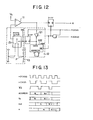
- FIG. 11 Another preferred embodiment of a past record correcting/reading apparatus is shown in Fig. 11 as a schematic block diagram.
- the past scanning line information is once stored in the storage circuit, and the binary-quantizing level is controlled by changing the slice level based upon the information stored in the storage circuit.
- reference numeral 11 indicates a comparator for comparing the image information output with the slice level
- reference numeral 12 denotes a buffer memory circuit (simply referred to as a “storage circuit") for storing the photoelectric conversion information of the respective photosensitive elements corresponding to the scanning lines during the past scanning period (referred to as "past scanning line information").
- Reference numeral 13 represents a quantizing-level control circuit for determining the quantizing-level based upon the past scanning line information.
- the light reflected from the original document 5 illuminated by the light source 4 is converted via the lens 3 by the image sensor 1 (e.g., a CdS image sensor) into photoelectric conversion output.
- the conversion output is amplified in the amplifier 2 and then transferred to the comparator 11.
- the comparated output is further binary-quantized.
- the resultant binary-quantized or binary-encoded signal appears at the output terminal "e" of the comparator 11.
- FIG. 12 A major circuit portion of the circuit shown in Fig. 11 is shown in Fig. 12.
- the binary-quantized output signal obtained by the comparator 11 is simultaneously written via a three-state buffer 121 of the storage circuit 12 into predetermined addresses of the RAM 122, as the past scanning line information, under the timing control shown in Fig. 13.
- the above binary-quantized output signal is simultaneously stored as the past scanning line information into the storage circuit 12.
- the past scanning line information stored in this storage circuit 12 is read out when the succeeding scaning line information is input to the comparator 11.
- the past scanning line information (referred to as " preceding scanning line information") is read from the RAM 122, and thereafter input into an analog switch 131 cf the quantizing-level control circuit 13. Then, the voltage levels appearing at point P in response to the past scanning line information stored in the RAM 122 are switched by the analog switch 131. As a result, the outputs of the quantizing-level control circuit 13 are changed according to value shown in Table 3 in response to the content of white "1" or black "0" of the read preceding scanning line information.
- the slice level of the comparator 11 is set to 25%, whereas when it is black “0", then the slice level is set to 75% so as to wait for the succeeding scanning line information because of the binary-quantization operation for the later information.
- the slice level is forecasted based upon the preceding scanning line information and the forecasted slice level is used as the binary-quantizing level in the preferred embodiment.
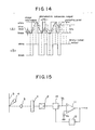
- Figs. 14A and 14B are waveforms for explaining a relationship between the image information variations and the photoelectric conversion output derived from the specific photosensitive element in the sub-scanning direction.
- a dash-dotted line represents the slice level and black points are sampling points for determining the binary-quantizing operation.
- FIG. 15 a schematic block diagram of Fig. 15, a description will be made of still another preferred embodiment.
- the same reference numerals shown in Fig. 11 are used for indicating the same or similar circuit elements of Fig. 15.
- Reference numeral 14 indicates a gain control circuit for controlling the signal level of the photoelectric conversion output conducted to the comparator 11 in accordance with the past scanning line information. Alternatively, such a gain control function may be involved in the amplifier 2. A voltage Vr for determining the binary-quantizing level of the comparator 11 is kept constant.
- the gain of the photoelectric conversion and amplification system can be controlled by conducting the preceding scanning line information stored in the storage circuit 12 to the gain control circuit 14 with keeping the slice level of the comparator 11 constant in the preferred embodiment. Relatively changing the slice level by varying the image signal level enables the same advantage as in the preferred embodiment of Fig. 11 to be achieved.
- the relative gain is controlled based upon the contents of the preceding scanning line information as listed in Table 4.
- the amplified image signal is twice as high as the original image signal and the level of the image signal is increased.
- the image signal is amplified by 2 / 3 times higher than the original image signal and the level of the image signal is decreased.
- the image signal amplified by different amplification is conducted into the comparator 11 having a constant signal level to be binary-quantilized, so that the binary-quantilized signal is derived from the output terminal "e" of the comparator 11.
- the corrected signal of the circuit according to the preferred embodiment is obtained as shown in Fig. 16A, so that even if the slice level is set constant, the waveform of the binary-quantized signal as shown in Fig. 16A can be realized. Because this waveform is the same as the waveform shown in Fig. 14B, the same advantage as in the previous embodiment may be achieved.
- the scanning line information (preceding scanning line information) immediately before the present scanning line information only was used as the past scanning line information. It is however possible to employ as the past scanning line information the scanning line information (referred to as "past previous scanning line information") before this preceding scanning line information for the purposes of the high speed scanning as well as the scanning stability.
- Fig. 17 another preferred embodiment will be described in which the preceding scanning line information and the past previous scanning line information are utilized as the past scanning line information.
- binary-quantizing level or relative gain, or both of them may be controlled to obtain the desired slice level
- binary-quantizing livel slice level
- the circuit arrangement is made here. It is however required to employ as the storage circuit 12 a storage circuit having a sufficient capacity capable of storing two sorts of the scanning line information, i.e., the preceding and also past previous scanning line information.
- a combination between the above two sets of scanning line information is preset as shown in Table 5.
- the binary-quantizing level control circuit 13 delivers the slice level signal preset by 20% to the comparator 11 (negative terminal) so as to wait for the succeeding information.
- the slice level is set by 50%, whereas if it is white "1" and white "1", the slice level is set by 80% for the preparation of the next scanning line information.
- the slice level (dashed-dotted line) varies so that the precise binary-quantized signal of the original image information (see Fig. 17B).
- the voltage difference between the sampling points (black point) for determining the binary-quantization and the slice level (dashed-dotted line) can be set greater than that of Fie. 14A, resulting in the stability of the operation. Consequently, more higher scanning operation can be realized (even when the scanning time periods are ⁇ /2, and ⁇ /3, the precise past record correction can be accomplished).
- the quantizing level may be controlled by the preceding scanning line information, while the relative gain may be controlled by the past previous scanning line information.
- the previous preferred embodiments employed the binary-quantizing or binary-encoding level, but may utilize the multi-level quantization.
- the multi-level quantization for instance, an A/D-converter for multi-leveled inputs and a memory capable of storing the multi-leveled input data. Either the quantizing level or the relative gain is changed in combination with precise control for the half tone information during the past record correction.
- the more precise correction can be achieved by introducing correction by the multi-leveled information, as compared with the binary-quantizing correction.
- the digital signal transmission system was introduced, but the analog signal transmission system may be utilized.
- the output level of the photoelectric conversion output signal is controlled and then is conducted to a modulator so that the substrantially same advantage as in the digital transmission system may be achieved.
Landscapes
- Engineering & Computer Science (AREA)
- Multimedia (AREA)
- Signal Processing (AREA)
- Facsimile Image Signal Circuits (AREA)
- Facsimile Scanning Arrangements (AREA)
Applications Claiming Priority (4)
| Application Number | Priority Date | Filing Date | Title |
|---|---|---|---|
| JP60233769A JP2506643B2 (ja) | 1985-10-18 | 1985-10-18 | 前歴補正読取装置 |
| JP233769/85 | 1985-10-18 | ||
| JP238050/85 | 1985-10-24 | ||
| JP60238050A JP2529193B2 (ja) | 1985-10-24 | 1985-10-24 | 前歴補正読取装置 |
Publications (3)
| Publication Number | Publication Date |
|---|---|
| EP0220069A2 true EP0220069A2 (de) | 1987-04-29 |
| EP0220069A3 EP0220069A3 (en) | 1988-09-28 |
| EP0220069B1 EP0220069B1 (de) | 1991-01-09 |
Family
ID=26531189
Family Applications (1)
| Application Number | Title | Priority Date | Filing Date |
|---|---|---|---|
| EP86308072A Expired EP0220069B1 (de) | 1985-10-18 | 1986-10-17 | Korrektur-/Lesegerät bezogen auf eine vorangegangene Aufzeichnung |
Country Status (3)
| Country | Link |
|---|---|
| US (1) | US4812667A (de) |
| EP (1) | EP0220069B1 (de) |
| DE (1) | DE3676784D1 (de) |
Cited By (1)
| Publication number | Priority date | Publication date | Assignee | Title |
|---|---|---|---|---|
| GB2226734A (en) * | 1988-12-05 | 1990-07-04 | Mitsubishi Electric Corp | Digital binarization circuit for conversion of image data |
Families Citing this family (2)
| Publication number | Priority date | Publication date | Assignee | Title |
|---|---|---|---|---|
| US5121230A (en) * | 1987-01-19 | 1992-06-09 | Canon Kabushiki Kaisha | Image reading apparatus having adjusting circuits for matching the level of and compensating for fluctuation among a plurality of sensing elements |
| JPS63301674A (ja) * | 1987-05-30 | 1988-12-08 | Ricoh Co Ltd | ラインセンサの信号前処理回路 |
Citations (2)
| Publication number | Priority date | Publication date | Assignee | Title |
|---|---|---|---|---|
| JPS56102161A (en) | 1980-01-18 | 1981-08-15 | Nec Corp | Binary encoding circuit |
| EP0064557A1 (de) | 1980-11-17 | 1982-11-17 | Fujitsu Limited | Verfahren zum Lesen eines Bildsignals |
Family Cites Families (3)
| Publication number | Priority date | Publication date | Assignee | Title |
|---|---|---|---|---|
| JPS54146528A (en) * | 1978-05-09 | 1979-11-15 | Nec Corp | Electron distribution recording device |
| US4453268A (en) * | 1981-03-18 | 1984-06-05 | Lundy Electronics & Systems, Inc. | OCR Page reader |
| JPS6184967A (ja) * | 1984-10-03 | 1986-04-30 | Oki Electric Ind Co Ltd | スライスレベル決定回路 |
-
1986
- 1986-10-17 EP EP86308072A patent/EP0220069B1/de not_active Expired
- 1986-10-17 DE DE8686308072T patent/DE3676784D1/de not_active Expired - Lifetime
- 1986-10-20 US US06/920,795 patent/US4812667A/en not_active Expired - Lifetime
Patent Citations (2)
| Publication number | Priority date | Publication date | Assignee | Title |
|---|---|---|---|---|
| JPS56102161A (en) | 1980-01-18 | 1981-08-15 | Nec Corp | Binary encoding circuit |
| EP0064557A1 (de) | 1980-11-17 | 1982-11-17 | Fujitsu Limited | Verfahren zum Lesen eines Bildsignals |
Cited By (3)
| Publication number | Priority date | Publication date | Assignee | Title |
|---|---|---|---|---|
| GB2226734A (en) * | 1988-12-05 | 1990-07-04 | Mitsubishi Electric Corp | Digital binarization circuit for conversion of image data |
| US5166808A (en) * | 1988-12-05 | 1992-11-24 | Mitsubishi Denki Kabushiki Kaisha | Digital binarization circuit for conversion of image data |
| GB2226734B (en) * | 1988-12-05 | 1993-05-12 | Mitsubishi Electric Corp | Digital binarization circuit for conversion of image data |
Also Published As
| Publication number | Publication date |
|---|---|
| EP0220069A3 (en) | 1988-09-28 |
| EP0220069B1 (de) | 1991-01-09 |
| DE3676784D1 (de) | 1991-02-14 |
| US4812667A (en) | 1989-03-14 |
Similar Documents
| Publication | Publication Date | Title |
|---|---|---|
| US4903143A (en) | Image processing apparatus | |
| US4554583A (en) | Shading correction device | |
| EP0039899B1 (de) | System zur Verarbeitung von Abtastsignalen | |
| JPH0357674B2 (de) | ||
| US4578711A (en) | Video data signal digitization and correction system | |
| US4570186A (en) | Binary transformation method | |
| US4853792A (en) | Image signal binary encoder | |
| US4841376A (en) | Shading correcting method enabling prevention of effect of noise and apparatus therefor | |
| US4367457A (en) | Signal processing apparatus | |
| US4812667A (en) | Past record correcting/reading apparatus | |
| JPS6340071B2 (de) | ||
| US4783836A (en) | Information reading apparatus | |
| EP1156664B1 (de) | Bildlesevorrichtung und Bilderzeugungsgerät | |
| US5115327A (en) | Gain control circuit for use in shading compensation circuit | |
| US4674126A (en) | Image signal processing apparatus | |
| US4473847A (en) | Binary coding system | |
| US5278672A (en) | Image signal processing apparatus | |
| JP2506643B2 (ja) | 前歴補正読取装置 | |
| GB2154827A (en) | Method for correcting picture signals in image input equipment | |
| JPH04271667A (ja) | 色彩情報の読み取り方式 | |
| JP2529193B2 (ja) | 前歴補正読取装置 | |
| JP2915448B2 (ja) | イメージセンサの2値化出力方法 | |
| JP2618655B2 (ja) | 画像読み取り装置 | |
| US5093733A (en) | Image signal processing device | |
| JPH0354510B2 (de) |
Legal Events
| Date | Code | Title | Description |
|---|---|---|---|
| PUAI | Public reference made under article 153(3) epc to a published international application that has entered the european phase |
Free format text: ORIGINAL CODE: 0009012 |
|
| AK | Designated contracting states |
Kind code of ref document: A2 Designated state(s): DE FR GB SE |
|
| PUAL | Search report despatched |
Free format text: ORIGINAL CODE: 0009013 |
|
| AK | Designated contracting states |
Kind code of ref document: A3 Designated state(s): DE FR GB SE |
|
| 17P | Request for examination filed |
Effective date: 19890328 |
|
| 17Q | First examination report despatched |
Effective date: 19890728 |
|
| GRAA | (expected) grant |
Free format text: ORIGINAL CODE: 0009210 |
|
| AK | Designated contracting states |
Kind code of ref document: B1 Designated state(s): DE FR GB SE |
|
| REF | Corresponds to: |
Ref document number: 3676784 Country of ref document: DE Date of ref document: 19910214 |
|
| ET | Fr: translation filed | ||
| PLBE | No opposition filed within time limit |
Free format text: ORIGINAL CODE: 0009261 |
|
| STAA | Information on the status of an ep patent application or granted ep patent |
Free format text: STATUS: NO OPPOSITION FILED WITHIN TIME LIMIT |
|
| 26N | No opposition filed | ||
| EAL | Se: european patent in force in sweden |
Ref document number: 86308072.7 |
|
| REG | Reference to a national code |
Ref country code: GB Ref legal event code: 746 Effective date: 19960819 |
|
| PGFP | Annual fee paid to national office [announced via postgrant information from national office to epo] |
Ref country code: SE Payment date: 20001009 Year of fee payment: 15 Ref country code: DE Payment date: 20001009 Year of fee payment: 15 |
|
| PGFP | Annual fee paid to national office [announced via postgrant information from national office to epo] |
Ref country code: FR Payment date: 20001010 Year of fee payment: 15 |
|
| PGFP | Annual fee paid to national office [announced via postgrant information from national office to epo] |
Ref country code: GB Payment date: 20001011 Year of fee payment: 15 |
|
| PG25 | Lapsed in a contracting state [announced via postgrant information from national office to epo] |
Ref country code: GB Free format text: LAPSE BECAUSE OF NON-PAYMENT OF DUE FEES Effective date: 20011017 |
|
| PG25 | Lapsed in a contracting state [announced via postgrant information from national office to epo] |
Ref country code: SE Free format text: LAPSE BECAUSE OF NON-PAYMENT OF DUE FEES Effective date: 20011018 |
|
| REG | Reference to a national code |
Ref country code: GB Ref legal event code: IF02 |
|
| EUG | Se: european patent has lapsed |
Ref document number: 86308072.7 |
|
| GBPC | Gb: european patent ceased through non-payment of renewal fee |
Effective date: 20011017 |
|
| PG25 | Lapsed in a contracting state [announced via postgrant information from national office to epo] |
Ref country code: FR Free format text: LAPSE BECAUSE OF NON-PAYMENT OF DUE FEES Effective date: 20020628 |
|
| PG25 | Lapsed in a contracting state [announced via postgrant information from national office to epo] |
Ref country code: DE Free format text: LAPSE BECAUSE OF NON-PAYMENT OF DUE FEES Effective date: 20020702 |
|
| REG | Reference to a national code |
Ref country code: FR Ref legal event code: ST |