EP0220210B1 - Elektrischer steckverbinder für ein elektrisches kabel - Google Patents
Elektrischer steckverbinder für ein elektrisches kabel Download PDFInfo
- Publication number
- EP0220210B1 EP0220210B1 EP86902232A EP86902232A EP0220210B1 EP 0220210 B1 EP0220210 B1 EP 0220210B1 EP 86902232 A EP86902232 A EP 86902232A EP 86902232 A EP86902232 A EP 86902232A EP 0220210 B1 EP0220210 B1 EP 0220210B1
- Authority
- EP
- European Patent Office
- Prior art keywords
- ground
- contacts
- signal
- disposed
- signal contacts
- Prior art date
- Legal status (The legal status is an assumption and is not a legal conclusion. Google has not performed a legal analysis and makes no representation as to the accuracy of the status listed.)
- Expired - Lifetime
Links
- 239000004020 conductor Substances 0.000 claims description 9
- 230000005540 biological transmission Effects 0.000 description 5
- 239000002184 metal Substances 0.000 description 5
- 230000000712 assembly Effects 0.000 description 4
- 238000000429 assembly Methods 0.000 description 4
- 239000011810 insulating material Substances 0.000 description 4
- 238000000034 method Methods 0.000 description 4
- 238000000465 moulding Methods 0.000 description 3
- 239000000758 substrate Substances 0.000 description 3
- 238000010276 construction Methods 0.000 description 2
- 230000003247 decreasing effect Effects 0.000 description 2
- 238000003780 insertion Methods 0.000 description 2
- 230000037431 insertion Effects 0.000 description 2
- 238000004806 packaging method and process Methods 0.000 description 2
- 238000002360 preparation method Methods 0.000 description 2
- 230000007423 decrease Effects 0.000 description 1
- 230000000694 effects Effects 0.000 description 1
- 238000004519 manufacturing process Methods 0.000 description 1
- 230000013011 mating Effects 0.000 description 1
Images


Classifications
-
- H—ELECTRICITY
- H01—ELECTRIC ELEMENTS
- H01R—ELECTRICALLY-CONDUCTIVE CONNECTIONS; STRUCTURAL ASSOCIATIONS OF A PLURALITY OF MUTUALLY-INSULATED ELECTRICAL CONNECTING ELEMENTS; COUPLING DEVICES; CURRENT COLLECTORS
- H01R12/00—Structural associations of a plurality of mutually-insulated electrical connecting elements, specially adapted for printed circuits, e.g. printed circuit boards [PCB], flat or ribbon cables, or like generally planar structures, e.g. terminal strips, terminal blocks; Coupling devices specially adapted for printed circuits, flat or ribbon cables, or like generally planar structures; Terminals specially adapted for contact with, or insertion into, printed circuits, flat or ribbon cables, or like generally planar structures
- H01R12/70—Coupling devices
- H01R12/77—Coupling devices for flexible printed circuits, flat or ribbon cables or like structures
- H01R12/78—Coupling devices for flexible printed circuits, flat or ribbon cables or like structures connecting to other flexible printed circuits, flat or ribbon cables or like structures
-
- H—ELECTRICITY
- H01—ELECTRIC ELEMENTS
- H01R—ELECTRICALLY-CONDUCTIVE CONNECTIONS; STRUCTURAL ASSOCIATIONS OF A PLURALITY OF MUTUALLY-INSULATED ELECTRICAL CONNECTING ELEMENTS; COUPLING DEVICES; CURRENT COLLECTORS
- H01R12/00—Structural associations of a plurality of mutually-insulated electrical connecting elements, specially adapted for printed circuits, e.g. printed circuit boards [PCB], flat or ribbon cables, or like generally planar structures, e.g. terminal strips, terminal blocks; Coupling devices specially adapted for printed circuits, flat or ribbon cables, or like generally planar structures; Terminals specially adapted for contact with, or insertion into, printed circuits, flat or ribbon cables, or like generally planar structures
- H01R12/70—Coupling devices
- H01R12/77—Coupling devices for flexible printed circuits, flat or ribbon cables or like structures
- H01R12/771—Details
- H01R12/775—Ground or shield arrangements
-
- H—ELECTRICITY
- H01—ELECTRIC ELEMENTS
- H01R—ELECTRICALLY-CONDUCTIVE CONNECTIONS; STRUCTURAL ASSOCIATIONS OF A PLURALITY OF MUTUALLY-INSULATED ELECTRICAL CONNECTING ELEMENTS; COUPLING DEVICES; CURRENT COLLECTORS
- H01R12/00—Structural associations of a plurality of mutually-insulated electrical connecting elements, specially adapted for printed circuits, e.g. printed circuit boards [PCB], flat or ribbon cables, or like generally planar structures, e.g. terminal strips, terminal blocks; Coupling devices specially adapted for printed circuits, flat or ribbon cables, or like generally planar structures; Terminals specially adapted for contact with, or insertion into, printed circuits, flat or ribbon cables, or like generally planar structures
- H01R12/50—Fixed connections
- H01R12/59—Fixed connections for flexible printed circuits, flat or ribbon cables or like structures
-
- H—ELECTRICITY
- H01—ELECTRIC ELEMENTS
- H01R—ELECTRICALLY-CONDUCTIVE CONNECTIONS; STRUCTURAL ASSOCIATIONS OF A PLURALITY OF MUTUALLY-INSULATED ELECTRICAL CONNECTING ELEMENTS; COUPLING DEVICES; CURRENT COLLECTORS
- H01R12/00—Structural associations of a plurality of mutually-insulated electrical connecting elements, specially adapted for printed circuits, e.g. printed circuit boards [PCB], flat or ribbon cables, or like generally planar structures, e.g. terminal strips, terminal blocks; Coupling devices specially adapted for printed circuits, flat or ribbon cables, or like generally planar structures; Terminals specially adapted for contact with, or insertion into, printed circuits, flat or ribbon cables, or like generally planar structures
- H01R12/70—Coupling devices
- H01R12/77—Coupling devices for flexible printed circuits, flat or ribbon cables or like structures
-
- H—ELECTRICITY
- H01—ELECTRIC ELEMENTS
- H01R—ELECTRICALLY-CONDUCTIVE CONNECTIONS; STRUCTURAL ASSOCIATIONS OF A PLURALITY OF MUTUALLY-INSULATED ELECTRICAL CONNECTING ELEMENTS; COUPLING DEVICES; CURRENT COLLECTORS
- H01R13/00—Details of coupling devices of the kinds covered by groups H01R12/70 or H01R24/00 - H01R33/00
- H01R13/646—Details of coupling devices of the kinds covered by groups H01R12/70 or H01R24/00 - H01R33/00 specially adapted for high-frequency, e.g. structures providing an impedance match or phase match
- H01R13/6461—Means for preventing cross-talk
- H01R13/6471—Means for preventing cross-talk by special arrangement of ground and signal conductors, e.g. GSGS [Ground-Signal-Ground-Signal]
-
- H—ELECTRICITY
- H01—ELECTRIC ELEMENTS
- H01R—ELECTRICALLY-CONDUCTIVE CONNECTIONS; STRUCTURAL ASSOCIATIONS OF A PLURALITY OF MUTUALLY-INSULATED ELECTRICAL CONNECTING ELEMENTS; COUPLING DEVICES; CURRENT COLLECTORS
- H01R13/00—Details of coupling devices of the kinds covered by groups H01R12/70 or H01R24/00 - H01R33/00
- H01R13/648—Protective earth or shield arrangements on coupling devices, e.g. anti-static shielding
- H01R13/658—High frequency shielding arrangements, e.g. against EMI [Electro-Magnetic Interference] or EMP [Electro-Magnetic Pulse]
- H01R13/6581—Shield structure
- H01R13/6585—Shielding material individually surrounding or interposed between mutually spaced contacts
Definitions
- This invention relates to an electrical connector for terminating electric cables such as a transmission cable which is used for the internal signal wiring of a computer or the like and particularly connecting to a post header mounted on the printed circuit board.
- a transmission cable for the internal signal wiring of a computer has a plurality of signal wires.
- the arrangement of the signal wires in an insulating jacket of the cable gives rise to a problem of crosstalk, i.e., unwanted exchange of signals between the adjacent signal wires.
- An electric cable is known which comprises a plurality of signal wires disposed in parallel to one another in a plane in an insulating jacket and a plurality of ground wires each disposed between alternate adjoining or adjacent signal wires to provide protection against crosstalk.
- an object of this invention to provide an electrical connector which can satisfactorily prevent the crosstalk between signal contacts without decreasing the density required to accommodate increased cable size in the number of signal conductors.
- an electrical connector for connection to signal conductors and ground conductors of an electrical cable comprising an insulating housing member having signal contact members and ground contact members disposed therein for electrical connection respectively to the signal conductors and ground conductors of the electrical cable and wherein said signal contacts are disposed in said housing member in two rows and have contact sections at a front end of said housing member for electrical connection with respective signal terminal members; said ground contacts are disposed in a row between said two rows of said signal contacts and have contact sections at said front end of said housing member for electrical connection with respective ground terminal members; and wherein a shield plate member is disposed in said housing member between said two rows of said signal contacts, said shield plate member and said ground contacts are a unitary ground member with said shield plate member defining a plate element disposed intermediate the signal contacts.
- the shield plate member is moulded into dielectric members and is in the form of an undivided plate extending between only the rear end portions of the signal contacts, the ground contacts being in the form of "tuning forks" projecting from a forward edge of the plate member and being formed integrally therewith.
- An electrical connector according to the present invention is characterized in that said shield plate member defines a plurality of plate elements disposed between aligned signal contacts, said plate elements and said ground contacts alternating with one another to prevent crosstalk between the signal contacts; and by ground base members including bifurcated front ends for receiving base ends of said ground contacts, said base ends of said ground contacts including resilient contacts press fitted within said bifurcated front ends of said ground base members.
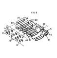
- FIG 1 is a perspective view of an electrical connector 2 embodying this invention and is electrically connected to a transmission cable 1 which is used for the internal wiring of a computer, or the like.
- Transmission cable 1 includes a plurality of signal wires S and a plurality of ground wires G which are disposed in mutually parallel and alternating relation in an insulating jacket 1a, as shown in Figure 2A. It is alternatively possible to dispose two ground wires G between every two adjacent signal wires S, as shown in Figure 2B. In either event, ground wires G shield adjacent signal wires S from each other to prevent any crosstalk therebetween.
- Electrical connector 2 includes a plurality of signal contacts and a plurality of ground contacts disposed in a housing 10 formed from a suitable insulating material.
- the signal contacts are to be connected to the signal wires in the cable, and the ground contacts are to be connected to the ground wires.
- the terminating portions terminated to the signal and ground wires are surrounded by an upper cover 3a and a lower cover 3b which include strain relief sections 3a' and 3b' that engage cable 1.
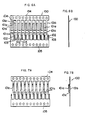
- Housing 10 has a front end wall 10a provided with holes through which male terminals are inserted for making contact with contact portions of the signal and ground contacts.
- the holes are provided in three rows one above another. Holes 11 in the upper row and holes 12 in the lower row as shown in Figure 3 are used for the insertion of male terminals 5,6 for making electrical contact with the signal contacts. Holes 13 in the middle row are used for the insertion of male terminals 7 for making electrical contact with the ground contacts. Holes 13 are provided in staggered relation with respect to holes 11 and 12, so that the spacing between the male terminals may be maximized to facilitate wiring located on the printed substrate on which the male terminals are preferably disposed. if the male terminals to be inserted have a large spacing therebetween, holes 13 do not necessarily need to be arranged in staggered relation relative to the other holes, but they can be arranged in a grid pattern.
- the staggered arrangement has the advantage of enabling the addition of the male terminals for making electrical contact with the ground contacts without any change having to be made in the conventional arrangement of the male terminals for making electrical contact with the signal contacts. This renders it no longer necessary to use a part of the male signal terminals as ground terminals. Therefore, the connector has a high packaging density.
- Housing 10 is provided therein with a plurality of upper signal contacts 20 and a plurality of lower signal contacts 30.
- Each of contacts 20 has a bifurcated contact end 22 facing one of upper holes 11 and each of contacts 30 has a bifurcated contact end 32 facing one of lower holes 12.
- Opposite or base ends 21 and 31 of contacts 20 and 30, respectively, are secured by insert molding in a holding member 40 made of a suitable insulating material.
- Holding member 40 has an upper projection 41 and a lower projection 42 which are fitted in the slots 15 formed in housing 10, whereby holding member 40 is secured to housing 10.
- An extreme end 23 of each contact 20 and an extreme end 33 (see Figure 12A) of each contact 30 project backwardly from holding member 40.
- One of signal wires S in cable 1 is connected to each of the ends 23, 33 of contacts 20, 30 in the area surrounded by upper and lower covers 3a and 3b.
- upper and lower signal contacts 20 and 30 may be joined together, they are spaced apart from each other in a direction perpendicular to the sheet of the drawing as shown in Figure 12A and contacts 20 and 30 are connected to different signal wires S.
- a shielding plate 61 is provided between upper and lower signal contacts 20 and 30 and is mounted on support member 61 a of housing 10.
- Shielding plate 61 forms an integral part of ground contacts 62, which are shown in Figures 4 and 5, and extends in the direction in which the ground contacts are arranged. Shielding plate 61 is grounded and thereby prevents any crosstalk between contacts 20 and 30.
- Contacts 20 and 30 are stamped and formed from a suitable metal having desirable spring characteristics and contact ends 22 and 32 thereof resiliently flex to receive male signal terminals 5 and 6 inserted through holes 11 and 12 of housing 10 to establish electrical contact therewith. As bifurcated contact ends 22 and 32 are moved apart by male terminals 5 and 6 and are likely to engage shielding plate 61, those surfaces of shielding plate 61 which face ends 22 and 32 are each coated with a suitable insulating film 61a which prevents the grounding of the signal transmitted through contacts 20 or 30 even if ends 22 or 32 may engage shielding plate 61.
- ground base members 50 are secured in holding member 40 in housing 10.
- Each ground base member 50 has a rear terminating end 52 to which one of ground wires G in cable 1 is connected.
- Ground base member 50 has bifurcated front ends 51 between which resilient contacts 65 of base end 63 is secured. Base end 63 is resiliently held in position when resilient contacts 65 are press-fitted between front ends 51.
- Each ground contact 62 has a contact end 64 which resiliently flex to receive male ground terminal 7 inserted through one of holes 13 for making electrical contact with terminal 7 and thereby connecting the corresponding ground wire G in cable 1 to ground.
- ground contact 62 is integral with shielding plate 61, they are both connected to ground by male terminal 7 and thereby effectively prevent crosstalk between signal contacts 20 and 30.
- Figure 5 is a perspective view of the upper and lower signal contacts 20 and 30, ground contacts 62 and shielding plate 61 disposed in housing 10.
- Upper signal contacts 20 lie in a row aligned with the upper row of holes 11, and the lower signal contacts 30 form a row aligned with the lower row of holes 12.
- An integral ground plate 60 which comprises shielding plate 61 and ground contacts 62 are arranged between the upper row of signal contacts 20 and the lower row of signal contacts 30 in such a way that shielding plate 61 and ground contacts 62 are alternating relation in a row.
- Ground plate 60 having shielding plate 61 and ground contacts 62 is stamped and formed from a suitable metal having desirable spring characteristics and includes base end 63 including resilient contacts 65 which are to be press-fitted between front ends 51 of ground base member 50.
- a conductive metal plate 100 is formed in strip form shown in Figures 6A and 6B.
- Plate 100 has a plurality of pairs of strips 101a a and 101b b connected by a portion 101c and defining contact ends 22 or 23 of signal contacts 20 or 30.
- a pair of carrier strips 104 and 105 hold the contacts together during the manufacture thereof.
- a plurality of strips 102 extend from the lower carrier strip 105 and are used to form rear ends 21 of the signal contacts to which signal wires S in cable 1 are connected.
- a plurality of strips 103 which are narrower than strips 102 extend from carrier strip 105 and are used to form ground base members 50.
- each connecting portion 101c is bent at right angles to strip 101b and strip 101 a is bent at right angles to connection portion 101c, so that connection portion 101c forms a U-shaped configuration. Then, the outer end of strip 101a and the corresponding portion of strip 101 are bent as shown in Figure 7B so that they form the shape of contact end 22 of a signal contact.
- a first holding portion 42 is formed by insert molding of insulating material around the upper end portions of strips 102 and 103.
- First holding portion 42 has a serrated bottom surface 42a which will be used for positioning first holding portion 42 relative to another first holding portion 42' as shown in Figures 10-12 and as will hereinafter be described.
- upper carrier strip 104 is cut away from signal contacts 20, as shown in Figures 9A to 9C. Then, the inner end portions of strips 102 and 103 are bent as shown in Figure 9B.
- strips 103 and 103' which form the rear end 52 of ground base member 50, are joined together one upon the other, but strips 102 and 102' which form the rear ends of signal contacts 20 and 30, are spaced apart from each other between the adjoining strips 103.
- the second holding portion 43 is formed by insert molding of a suitable insulating material under first holding portions 42 and 42' of assemblies 110 and 120 so that assemblies 110 and 120 are joined together, as shown in Figures 12A and 12B.
- First holding portions 42 and 42' and second holding portion 43 form holding member 40 shown in Figures 3 and 4.
- Lower carrier strip 105 is cut away and a connecting strip 53 holds the rear ends 52 of the ground base members 50, as shown in Figure 12A.
- Rear ends 23 and 33 of signal contacts 20 and 30 are located between adjoining rear ends 52 of base members 50 in mutually spaced apart relation.
- Front ends 51 of each base member 50 are defined by a pair of strips spaced apart from each other and projecting above holding member 40.
- FIG 13A is a front elevational view of ground plate 60 integrally having ground contacts 62 and shielding plates 61
- Figure 13B is a bottom plan view thereof.
- Ground plate 60 comprises a single metal plate bent to form a U-shaped cross section and is formed to include ground contacts 62 and shielding plates 61 in alternating relation, as shown in Figures 14 and 15, which are sectional views taken along the lines 14-14 and 15-15, respectively, of Figure 13A.
- the upper end of each ground contact 62 is bent to form contact end 64 for flexibly receiving male ground terminal 7 and lower base end 63 thereof has resilient contacts 65 extending outwardly therefrom at spaced intervals along base end 63.
- Each shielding plate 61 is defined by a pair of generally parallel strips, as shown in Figure 15.
- Ground plate 60 is placed between the two rows of signal contacts 20 and 30 in the assemblies shown in Figures 12A and 12B.
- the whole assembly including ground plate 60 is shown in Figures 16A and 16B.
- resilient contacts 65 of ground plate 60 are press-fitted between front ends 51 of base members 50 secured to and projecting upward from holding member 40, as shown in Figure 17, which is a cross-sectional view taken along the line 17-17 of Figure 16A.
- each shielding plate 61 is located between a pair of signal contacts 20 and 30, as shown in Figure 18, which is a cross-sectional view taken along the line 18-18 of Figure 16A.
- the electrical connector of this invention can also be used for connecting any other cable that requires shielding, including coaxial cable.
- This invention is characterized by including two rows of signal contacts and a row of ground plates disposed between the two rows of signal contacts.
- the ground plates shield adjoining signal contacts from each other and thereby prevent any crosstalk therebetween.
- Each ground contact is exclusively connected to a ground terminal and it is no longer necessary to employ a part of signal contacts for grounding purposes. Therefore, the electrical connector of this invention has a high packaging density.
Landscapes
- Details Of Connecting Devices For Male And Female Coupling (AREA)
- Multi-Conductor Connections (AREA)
- Coupling Device And Connection With Printed Circuit (AREA)
Claims (3)
dadurch gekennzeichnet, daß das Abschirmplattenelement (61) eine Mehrzahl von Plattenelementen definiert, die zwischen ausgerichteten Signalkontakten (20, 30) angeordnet sind, wobei die Plattenelemente und die Erdungskontakte (62) zur Verhinderung eines Nebensprechens zwischen den Signalkontakten (20, 30) in miteinander alternierender Weise angeordnet sind; sowie gekennzeichnet durch ein Erdungsbasiselement (50) mit gegabelten Vorderenden (51) zur Aufnahme von Basisenden (63) der Erdungskontakte (62), wobei die Basisenden (63) der Erdungskontakte (62) federnd nachgiebige Kontakte (65) aufweisen, die im Preßsitz in die gegabelten Vorderenden (51) der Erdungsbasiselemente (50) eingepaßt sind.
Applications Claiming Priority (2)
| Application Number | Priority Date | Filing Date | Title |
|---|---|---|---|
| JP60089878A JPS61248375A (ja) | 1985-04-25 | 1985-04-25 | 電気コネクタ |
| JP89878/85 | 1985-04-25 |
Publications (2)
| Publication Number | Publication Date |
|---|---|
| EP0220210A1 EP0220210A1 (de) | 1987-05-06 |
| EP0220210B1 true EP0220210B1 (de) | 1990-09-26 |
Family
ID=13983022
Family Applications (1)
| Application Number | Title | Priority Date | Filing Date |
|---|---|---|---|
| EP86902232A Expired - Lifetime EP0220210B1 (de) | 1985-04-25 | 1986-03-24 | Elektrischer steckverbinder für ein elektrisches kabel |
Country Status (7)
| Country | Link |
|---|---|
| US (1) | US4820175A (de) |
| EP (1) | EP0220210B1 (de) |
| JP (1) | JPS61248375A (de) |
| KR (1) | KR880700489A (de) |
| DE (1) | DE3674533D1 (de) |
| ES (1) | ES297000Y (de) |
| WO (1) | WO1986006553A1 (de) |
Families Citing this family (31)
| Publication number | Priority date | Publication date | Assignee | Title |
|---|---|---|---|---|
| US5094623A (en) * | 1991-04-30 | 1992-03-10 | Thomas & Betts Corporation | Controlled impedance electrical connector |
| US5122065A (en) * | 1991-08-12 | 1992-06-16 | International Business Machines Corp. | Input output connector with coaxial shielding and strain relief |
| NZ248262A (en) * | 1992-09-08 | 1995-08-28 | Whitaker Corp | Shielded connector for lan data cable end |
| US5584727A (en) * | 1992-09-08 | 1996-12-17 | The Whitaker Corporation | Shielded data connector |
| NL9202302A (nl) * | 1992-12-31 | 1994-07-18 | Du Pont Nederland | Koaxiaal interkonnektiesysteem. |
| US5577931A (en) * | 1994-07-25 | 1996-11-26 | Emc Corporation | Two-channel SCSI-compatible interconnect system and method |
| US5928028A (en) * | 1997-03-26 | 1999-07-27 | Quantum Corporation | Interspersed ground ribbon cable assemblies and methods therefor |
| JP3451393B2 (ja) | 1998-01-30 | 2003-09-29 | 日本航空電子工業株式会社 | プラグコネクタ及びソケットコネクタ |
| US7314377B2 (en) * | 1998-04-17 | 2008-01-01 | Fci Americas Technology, Inc. | Electrical power connector |
| US6319075B1 (en) | 1998-04-17 | 2001-11-20 | Fci Americas Technology, Inc. | Power connector |
| US20020098743A1 (en) * | 1998-04-17 | 2002-07-25 | Schell Mark S. | Power connector |
| US6217372B1 (en) | 1999-10-08 | 2001-04-17 | Tensolite Company | Cable structure with improved grounding termination in the connector |
| US6857899B2 (en) | 1999-10-08 | 2005-02-22 | Tensolite Company | Cable structure with improved grounding termination in the connector |
| KR100694401B1 (ko) * | 2000-03-31 | 2007-03-12 | 타이코 일렉트로닉스 에이엠피 케이.케이. | 전기 커넥터 조립체 |
| US6428344B1 (en) | 2000-07-31 | 2002-08-06 | Tensolite Company | Cable structure with improved termination connector |
| TW540187B (en) | 2000-09-29 | 2003-07-01 | Tyco Electronics Amp Kk | Electrical connector assembly and female connector |
| US6452107B1 (en) | 2000-11-10 | 2002-09-17 | Tensolite Company | Multiple pair, high speed data transmission cable and method of forming same |
| JP3877132B2 (ja) * | 2000-11-20 | 2007-02-07 | 富士通株式会社 | 多層配線基板及び半導体装置 |
| JP2002223513A (ja) * | 2001-01-24 | 2002-08-09 | Yazaki Corp | フラット電線の端末処理構造 |
| US20040147169A1 (en) * | 2003-01-28 | 2004-07-29 | Allison Jeffrey W. | Power connector with safety feature |
| US6848950B2 (en) | 2003-05-23 | 2005-02-01 | Fci Americas Technology, Inc. | Multi-interface power contact and electrical connector including same |
| JP4026605B2 (ja) * | 2004-03-01 | 2007-12-26 | 松下電工株式会社 | 電線接続用コネクタの製造方法 |
| US7376215B2 (en) * | 2005-12-27 | 2008-05-20 | Honeywell International Inc. | Measurement of ash composition using scanning high voltage X-ray sensor |
| US7549897B2 (en) | 2006-08-02 | 2009-06-23 | Tyco Electronics Corporation | Electrical connector having improved terminal configuration |
| US7591655B2 (en) | 2006-08-02 | 2009-09-22 | Tyco Electronics Corporation | Electrical connector having improved electrical characteristics |
| JP2009193786A (ja) * | 2008-02-13 | 2009-08-27 | Yamaichi Electronics Co Ltd | Hdmi規格ケーブル用コネクタ |
| US8177564B1 (en) | 2010-12-03 | 2012-05-15 | Yamaichi Electronics Co., Ltd. | Receptacle connector and an electrical connector using the same |
| DE102010063486A1 (de) * | 2010-12-20 | 2012-06-21 | Robert Bosch Gmbh | Elektrischer Steckverbinder mit vorgeordneter Kontaktklemme |
| US8337221B1 (en) * | 2011-09-20 | 2012-12-25 | Chicony Power Technology Co., Ltd. | Transmission apparatus |
| CN105659441B (zh) * | 2013-11-26 | 2018-01-23 | 申泰公司 | 直接附着的连接器 |
| EP3501066B1 (de) * | 2016-08-18 | 2021-08-18 | Samtec, Inc. | Direktsteckverbinder und herstellverfahren dafür |
Family Cites Families (6)
| Publication number | Priority date | Publication date | Assignee | Title |
|---|---|---|---|---|
| US4094564A (en) * | 1977-03-17 | 1978-06-13 | A P Products Incorporated | Multiple conductor electrical connector with ground bus |
| US4406512A (en) * | 1981-07-24 | 1983-09-27 | E. I. Du Pont De Nemours And Company | Triple row coax cable connector |
| US4451099A (en) * | 1982-05-07 | 1984-05-29 | Amp Incorporated | Electrical connector having commoning member |
| US4634211A (en) * | 1982-09-30 | 1987-01-06 | Leviton Manufacturing Company, Inc. | Wiring device system with single screw subassembly |
| US4641904A (en) * | 1983-06-18 | 1987-02-10 | Yamaichi Electric Mfg. Co., Ltd. | Flat cable connecting system |
| US4737117A (en) * | 1983-09-26 | 1988-04-12 | Amp Incorporated | Double-row electrical connector and method of making same |
-
1985
- 1985-04-25 JP JP60089878A patent/JPS61248375A/ja active Pending
-
1986
- 1986-03-24 EP EP86902232A patent/EP0220210B1/de not_active Expired - Lifetime
- 1986-03-24 DE DE8686902232T patent/DE3674533D1/de not_active Expired - Fee Related
- 1986-03-24 US US06/938,082 patent/US4820175A/en not_active Expired - Lifetime
- 1986-03-24 KR KR860700929A patent/KR880700489A/ko not_active Ceased
- 1986-03-24 WO PCT/US1986/000595 patent/WO1986006553A1/en not_active Ceased
- 1986-04-24 ES ES1986297000U patent/ES297000Y/es not_active Expired
Also Published As
| Publication number | Publication date |
|---|---|
| ES297000U (es) | 1988-03-16 |
| WO1986006553A1 (en) | 1986-11-06 |
| EP0220210A1 (de) | 1987-05-06 |
| JPS61248375A (ja) | 1986-11-05 |
| ES297000Y (es) | 1988-11-16 |
| US4820175A (en) | 1989-04-11 |
| KR880700489A (ko) | 1988-03-15 |
| DE3674533D1 (de) | 1990-10-31 |
Similar Documents
| Publication | Publication Date | Title |
|---|---|---|
| EP0220210B1 (de) | Elektrischer steckverbinder für ein elektrisches kabel | |
| EP0270598B1 (de) | Abgeschirmter elektrischer verbinder | |
| US5865646A (en) | Connector shield with integral latching and ground structure | |
| EP0918376B1 (de) | Moduläre Steckverbinder und deren Herstellungsverfahren | |
| US7874849B2 (en) | Plug for shielded data cables | |
| EP0555963B1 (de) | Stecker mit einteiligem Massestreifen | |
| KR940011264B1 (ko) | 접지 구조물을 갖고 있는 커넥터 | |
| US6641438B1 (en) | High speed, high density backplane connector | |
| US6250935B1 (en) | Electrical connector | |
| US5380223A (en) | High density electrical connector | |
| US6808419B1 (en) | Electrical connector having enhanced electrical performance | |
| EP0107288B1 (de) | Elektrischer Verbinderzusammenbau zum Anschliessen eines elektrischen abgeschirmten Flachkabels | |
| EP0836249B1 (de) | Elektrische Erdungshülle | |
| KR910002264B1 (ko) | 다수의 전기 도체를 위한 종단기(terminator)와 그 중단기용 하우징 | |
| US20020168898A1 (en) | Electrical connector having differential pair terminals with equal length | |
| GB2392321A (en) | Connector for shielded electrical cables | |
| JPH06325829A (ja) | 電気コネクタ組立体 | |
| WO1987007441A1 (en) | Shielded electrical connector | |
| EP0455367B1 (de) | Rechtwinklig abgebogener impedanzangepasster Steckverbinder | |
| EP0109297B1 (de) | Elektrische Kontaktorgane und Zusammenbau elektrischer Verbinder | |
| EP0793312A2 (de) | Abgeschirmter leiterplattenmontierter elektrischer Verbinder | |
| US5190464A (en) | Shielded electrical connector with contact shunting arrangement | |
| JP2952690B2 (ja) | 高周波コネクタ | |
| JPS61163574A (ja) | 電気コネクタ装置 | |
| KR100558821B1 (ko) | 모듈라커넥터 |
Legal Events
| Date | Code | Title | Description |
|---|---|---|---|
| PUAI | Public reference made under article 153(3) epc to a published international application that has entered the european phase |
Free format text: ORIGINAL CODE: 0009012 |
|
| 17P | Request for examination filed |
Effective date: 19861222 |
|
| AK | Designated contracting states |
Kind code of ref document: A1 Designated state(s): DE FR GB IT NL |
|
| 17Q | First examination report despatched |
Effective date: 19890502 |
|
| RAP3 | Party data changed (applicant data changed or rights of an application transferred) |
Owner name: AMP INCORPORATED (A NEW JERSEY CORPORATION) |
|
| RAP1 | Party data changed (applicant data changed or rights of an application transferred) |
Owner name: AMP INCORPORATED |
|
| GRAA | (expected) grant |
Free format text: ORIGINAL CODE: 0009210 |
|
| AK | Designated contracting states |
Kind code of ref document: B1 Designated state(s): DE FR GB IT NL |
|
| XX | Miscellaneous (additional remarks) |
Free format text: DRUCKSCHRIFT W086/06553(PCT/US86/00595)WURDE BERICHTIGT:ZEICHNUNGEN BLATT 1/8 BIS 8/8 HINZUGEFUEGT. |
|
| ITF | It: translation for a ep patent filed | ||
| REF | Corresponds to: |
Ref document number: 3674533 Country of ref document: DE Date of ref document: 19901031 |
|
| ET | Fr: translation filed | ||
| PLBE | No opposition filed within time limit |
Free format text: ORIGINAL CODE: 0009261 |
|
| STAA | Information on the status of an ep patent application or granted ep patent |
Free format text: STATUS: NO OPPOSITION FILED WITHIN TIME LIMIT |
|
| 26N | No opposition filed | ||
| ITTA | It: last paid annual fee | ||
| REG | Reference to a national code |
Ref country code: GB Ref legal event code: 732E |
|
| PGFP | Annual fee paid to national office [announced via postgrant information from national office to epo] |
Ref country code: NL Payment date: 19970120 Year of fee payment: 12 |
|
| PGFP | Annual fee paid to national office [announced via postgrant information from national office to epo] |
Ref country code: GB Payment date: 19970205 Year of fee payment: 12 |
|
| PGFP | Annual fee paid to national office [announced via postgrant information from national office to epo] |
Ref country code: FR Payment date: 19970307 Year of fee payment: 12 |
|
| PGFP | Annual fee paid to national office [announced via postgrant information from national office to epo] |
Ref country code: DE Payment date: 19970326 Year of fee payment: 12 |
|
| PG25 | Lapsed in a contracting state [announced via postgrant information from national office to epo] |
Ref country code: GB Free format text: LAPSE BECAUSE OF NON-PAYMENT OF DUE FEES Effective date: 19980324 |
|
| PG25 | Lapsed in a contracting state [announced via postgrant information from national office to epo] |
Ref country code: FR Free format text: THE PATENT HAS BEEN ANNULLED BY A DECISION OF A NATIONAL AUTHORITY Effective date: 19980331 |
|
| PG25 | Lapsed in a contracting state [announced via postgrant information from national office to epo] |
Ref country code: NL Free format text: LAPSE BECAUSE OF NON-PAYMENT OF DUE FEES Effective date: 19981001 |
|
| GBPC | Gb: european patent ceased through non-payment of renewal fee |
Effective date: 19980324 |
|
| NLV4 | Nl: lapsed or anulled due to non-payment of the annual fee |
Effective date: 19981001 |
|
| PG25 | Lapsed in a contracting state [announced via postgrant information from national office to epo] |
Ref country code: DE Free format text: LAPSE BECAUSE OF NON-PAYMENT OF DUE FEES Effective date: 19981201 |
|
| REG | Reference to a national code |
Ref country code: FR Ref legal event code: ST |
|
| PG25 | Lapsed in a contracting state [announced via postgrant information from national office to epo] |
Ref country code: IT Free format text: LAPSE BECAUSE OF NON-PAYMENT OF DUE FEES Effective date: 20050324 |