EP0220511A2 - Circuit pour un détecteur à infrarouge pour contrôler des espaces - Google Patents
Circuit pour un détecteur à infrarouge pour contrôler des espaces Download PDFInfo
- Publication number
- EP0220511A2 EP0220511A2 EP86113333A EP86113333A EP0220511A2 EP 0220511 A2 EP0220511 A2 EP 0220511A2 EP 86113333 A EP86113333 A EP 86113333A EP 86113333 A EP86113333 A EP 86113333A EP 0220511 A2 EP0220511 A2 EP 0220511A2
- Authority
- EP
- European Patent Office
- Prior art keywords
- circuit arrangement
- operational amplifier
- field effect
- effect transistor
- constant current
- Prior art date
- Legal status (The legal status is an assumption and is not a legal conclusion. Google has not performed a legal analysis and makes no representation as to the accuracy of the status listed.)
- Granted
Links
Images
Classifications
-
- G—PHYSICS
- G08—SIGNALLING
- G08B—SIGNALLING SYSTEMS, e.g. PERSONAL CALLING SYSTEMS; ORDER TELEGRAPHS; ALARM SYSTEMS
- G08B13/00—Burglar, theft or intruder alarms
- G08B13/18—Actuation by interference with heat, light, or radiation of shorter wavelength; Actuation by intruding sources of heat, light, or radiation of shorter wavelength
- G08B13/189—Actuation by interference with heat, light, or radiation of shorter wavelength; Actuation by intruding sources of heat, light, or radiation of shorter wavelength using passive radiation detection systems
- G08B13/19—Actuation by interference with heat, light, or radiation of shorter wavelength; Actuation by intruding sources of heat, light, or radiation of shorter wavelength using passive radiation detection systems using infrared-radiation detection systems
Definitions
- the invention relates to a circuit arrangement for an infrared room surveillance detector with a sensor and a field effect transistor connected downstream thereof.
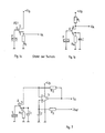
- Fig. 1a shows a known circuit of this type, in which one connection of a pyro element P is connected to ground or to the minus operating voltage terminal and the other connection is connected to the gate electrode of a field effect transistor (hereinafter abbreviated to FET).
- the drain electrode of the FET is connected to the positive operating voltage terminal U B.
- the source electrode of the FET is connected to ground via a resistor R A or to the minus operating voltage terminal -U B.
- the signal voltage U A is tapped via this resistor R A.
- the circuit shown is thus designed analogously to an emitter follower circuit.
- the signal voltage U A is very sensitive to interference voltages which are superimposed on the operating voltage U B , since such interference voltages also affect the gate voltage and thus the signal voltage U A due to the drain-gate reaction of the FET lies in the ⁇ V range.
- the operating voltage + U B applied to the drain electrode of the FET has noise or interference components in said ⁇ V range, so that the sensor signal cannot be evaluated with sufficient reliability for signaling. It is therefore necessary to sieve the operating voltage U B very well, ie it is a power supply unit with a high sieve factor 100 to 120 dB required. To maintain the high sieve factor, two power supplies are often connected in series. The circuit complexity for screening the operating voltage U B is therefore high.
- the invention is therefore based on the object of providing a circuit arrangement of the type mentioned at the outset which does not require a large amount of sieving in the power supply unit and which enables the sensor signal to be amplified in a simple manner.
- drain electrode of the FET is connected to the minus input of an operational amplifier, the output signal of which is fed back via a feedback resistor to the minus input of the operational amplifier.
- connection of an operational amplifier according to the invention and the specified circuit of the same in connection with the FET makes it possible to use the operational amplifier stabilization, which results in an attenuation of 80 to 100 dB.
- the drain voltage of the FET is automatically kept stable without additional circuitry for screening and there is therefore practically no reaction on the gate electrode of the FET.
- the operational amplifier circuit therefore automatically regulates all fluctuations in the mains voltage, the drain voltage of the FET remains constant, and this also results in an undisturbed useful signal or an undisturbed signal voltage.
- the operational amplifier in the circuit arrangement according to the invention is not connected as a voltage amplifier, but rather as a current amplifier, as a result of which fluctuations at the minus input of the operational amplifier and thus at the drain electrode of the FET are suppressed, with the result that interference effects on the gate -Electrode of the FET does not occur.
- C-MOS operational amplifiers are particularly suitable for this purpose.
- the use of less high-impedance operational amplifiers is also possible, in particular if the operating voltage is additionally sieved with a sieve factor of 20 to 30 dB, for example using an upstream power supply unit.
- a particularly advantageous embodiment of the invention consists in that the source electrode of the FET is provided with a constant current by means of a constant current source.
- the DC value of the output signal can be kept constant by using a constant current source.
- Another very advantageous possibility in connection with the present invention is to supply the constant current source with the output signal of the operational amplifier as a control signal.
- the output signal of the operational amplifier is thus fed back via the constant current source, so that the output voltage or the quiescent current value of the output voltage is kept stable.
- Another embodiment of the invention is to design the constant current source as a feedback quadrupole. It is particularly advantageous to provide an integration element for damping the useful signal in connection with the feedback quadrupole. This ensures that the entire circuit is operated in idle amplification.
- An embodiment in which the feedback quadrupole has an attenuator whose attenuation factor is regulated in proportion to the overall gain of the detector circuit arrangement is also advantageous. In this way, a constant amplification of the useful signal is ensured with the exclusion of manufacturing, component, temperature and other tolerances.
- the circuit arrangement can be produced particularly cost-effectively, since the simplest components with large tolerances can be used and still no adjustment is necessary.
- Circuit parts and components which correspond to FIGS. 2 to 4 chen, are provided with the same reference numerals.
- the gate electrode of a field effect transistor 2 is connected to a connection of a pyro element 1, the other connection of which is connected to ground or to the minus operating voltage source.
- the source electrode of the FET 2 is connected via a resistor R 1 and a capacitor C 1 connected in parallel to this resistor R 1, also to ground or to the minus operating voltage terminal.
- the drain electrode of the FET 2 is connected to the minus input of an operational amplifier 3, the plus input of which is connected to ground or to the minus operating voltage source via a capacitor C2.
- the plus input of the operational amplifier 3 is provided with a reference voltage U Ref via a resistor R3.
- the output signal S A of the operational amplifier 3 is fed back to the minus input of the operational amplifier 3 via a resistor R2.
- the resistance R2 is preferably in the mega-ohm range. For example, it has a resistance value of 1 MOhm.
- the operating voltage connections of the operational amplifier 3 are connected to the positive operating voltage terminal + U B or to the negative operating voltage terminal -U B or ground.
- the output signal of the pyroelement 1 occurring at the drain electrode of the FET 2 is amplified in the operational amplifier 3, and this amplified signal is fed back via the feedback branch containing the resistor R2 to the minus input of the operational amplifier 3. Since the operational amplifier itself has a good sieving effect of approximately 80 to 100 dB for the supply voltage, this property of the operational amplifier is used in addition to the actual gain property for the useful signal in order to keep the drain voltage of the FET 2 stable. As a result, there is also no negative reaction from the drain electrode to the gate electrode, so that the useful signal cannot be negatively influenced.
- the operational amplifier circuit regulates all fluctuations, so that the drain voltage remains completely constant. The useful signal is no longer subjected to voltage amplification, but rather to current amplification. As a result, the useful signal is free of fluctuations or interference components that may occur in the operating voltage.
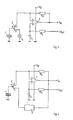
- the embodiment shown in Fig. 3 differs from the circuit arrangement in Fig. 2 only in that the existing from the resistor R1 and C1, in the source electrode branch of the FET 2 parallel circuit is now replaced by a constant current source 4. In this way, the direct current value of the useful signal S A can be kept constant even better.
- a constant current source or a feedback quadrupole 5 is provided in the source electrode branch of the FET 2, instead of a grounded constant current source 4 or a parallel circuit comprising a resistor R1 and a capacitor C1, the or the output signal S A of the operational amplifier 3 is supplied as a control signal. That is, the constant current source is fed back by means of the DC output voltage of the operational amplifier 3 in such a way that the DC voltage or quiescent voltage value of the output signal remains stable.
- the feedback quadrupole 5 can be designed, for example, in the form of an operational amplifier, transistor or current mirror circuit.
- the output signal of the feedback constant current source or of the feedback quadrupole 5 can be amplified before being fed into the source electrode of the FET 2.
- the integration element can be designed, for example, in the form of an operational amplifier with feedback via a capacitor. Furthermore, it is possible to design the feedback quadrupole as an attenuator whose attenuation factor is just as large as the total gain of the circuit arrangement should be.
Landscapes
- Physics & Mathematics (AREA)
- General Physics & Mathematics (AREA)
- Amplifiers (AREA)
- Radiation Pyrometers (AREA)
- Geophysics And Detection Of Objects (AREA)
- Burglar Alarm Systems (AREA)
- Fire-Detection Mechanisms (AREA)
- Photometry And Measurement Of Optical Pulse Characteristics (AREA)
Applications Claiming Priority (2)
| Application Number | Priority Date | Filing Date | Title |
|---|---|---|---|
| DE3537316A DE3537316C1 (de) | 1985-10-19 | 1985-10-19 | Schaltungsanordnung fuer einen Infrarot-Raumueberwachungsdetektor |
| DE3537316 | 1985-10-19 |
Publications (3)
| Publication Number | Publication Date |
|---|---|
| EP0220511A2 true EP0220511A2 (fr) | 1987-05-06 |
| EP0220511A3 EP0220511A3 (en) | 1987-10-07 |
| EP0220511B1 EP0220511B1 (fr) | 1991-02-06 |
Family
ID=6284011
Family Applications (1)
| Application Number | Title | Priority Date | Filing Date |
|---|---|---|---|
| EP86113333A Expired - Lifetime EP0220511B1 (fr) | 1985-10-19 | 1986-09-27 | Circuit pour un détecteur à infrarouge pour contrôler des espaces |
Country Status (4)
| Country | Link |
|---|---|
| US (1) | US4827133A (fr) |
| EP (1) | EP0220511B1 (fr) |
| JP (1) | JPS62100626A (fr) |
| DE (2) | DE3537316C1 (fr) |
Cited By (1)
| Publication number | Priority date | Publication date | Assignee | Title |
|---|---|---|---|---|
| CN104316174A (zh) * | 2014-10-31 | 2015-01-28 | 成都中远信电子科技有限公司 | 一种红外线光电检测电路 |
Families Citing this family (10)
| Publication number | Priority date | Publication date | Assignee | Title |
|---|---|---|---|---|
| NZ220217A (en) * | 1987-05-06 | 1991-03-26 | Graydon Aubrey Shepherd | Pyro-electric sensor circuit |
| JPH0530105Y2 (fr) * | 1987-05-29 | 1993-08-02 | ||
| US5034608A (en) * | 1989-09-08 | 1991-07-23 | Massachusetts Institute Of Technology | Infrared sensor operable without cooling |
| DE19619459C2 (de) * | 1996-05-14 | 2000-06-08 | Heimann Optoelectronics Gmbh | Schaltung zur Erfassung elektromagnetischer Strahlung |
| US6340816B1 (en) | 1998-02-27 | 2002-01-22 | Honeywell International, Inc. | Pyroelectric detector with feedback amplifier for enhanced low frequency response |
| JP4257989B2 (ja) * | 1998-10-19 | 2009-04-30 | 三菱電機株式会社 | 赤外線検出装置及びそれを用いた赤外線検出器アレイ |
| DE602004019898D1 (de) * | 2003-04-07 | 2009-04-23 | Microsystems On Silicon Pty Lt | Sensorvorrichtung für die erfassung eines physikalischen parameters |
| WO2012002496A1 (fr) * | 2010-07-01 | 2012-01-05 | パナソニック電工株式会社 | Dispositif de détection d'objets-cibles |
| JP2015049043A (ja) * | 2013-08-29 | 2015-03-16 | セイコーインスツル株式会社 | 赤外線検出装置 |
| CN115291552A (zh) * | 2022-08-25 | 2022-11-04 | 山西省农业机械发展中心 | 一种带智能保护的叶轮控制系统 |
Family Cites Families (8)
| Publication number | Priority date | Publication date | Assignee | Title |
|---|---|---|---|---|
| DE2113053A1 (de) * | 1970-03-19 | 1971-09-30 | Kureha Chemical Ind Co Ltd | Verfahren und Vorrichtung zum Steuern eines elektrischen Stromkreises |
| US3944859A (en) * | 1974-09-03 | 1976-03-16 | Rca Corporation | Bridge-balance detection circuit |
| US3987319A (en) * | 1974-12-05 | 1976-10-19 | The United States Of America As Represented By The Secretary Of The Army | Radiation-activated sensor |
| US4101767A (en) * | 1977-05-20 | 1978-07-18 | Sensors, Inc. | Discriminating fire sensor |
| US4367408A (en) * | 1979-01-17 | 1983-01-04 | Sanyo Electric Co., Ltd. | Pyroelectric type infrared radiation detecting device |
| US4267468A (en) * | 1979-04-23 | 1981-05-12 | Motorola, Inc. | Temperature sensing circuit |
| DE3404151A1 (de) * | 1984-02-07 | 1985-08-08 | Richard Hirschmann Radiotechnisches Werk, 7300 Esslingen | Meldeeinrichtung |
| US4618770A (en) * | 1985-03-21 | 1986-10-21 | Rca Corporation | Electrical controller having a window discriminator |
-
1985
- 1985-10-19 DE DE3537316A patent/DE3537316C1/de not_active Expired
-
1986
- 1986-09-27 DE DE8686113333T patent/DE3677456D1/de not_active Expired - Fee Related
- 1986-09-27 EP EP86113333A patent/EP0220511B1/fr not_active Expired - Lifetime
- 1986-10-20 US US06/920,383 patent/US4827133A/en not_active Expired - Fee Related
- 1986-10-20 JP JP61247666A patent/JPS62100626A/ja active Granted
Cited By (2)
| Publication number | Priority date | Publication date | Assignee | Title |
|---|---|---|---|---|
| CN104316174A (zh) * | 2014-10-31 | 2015-01-28 | 成都中远信电子科技有限公司 | 一种红外线光电检测电路 |
| CN104316174B (zh) * | 2014-10-31 | 2016-06-29 | 国网山东省电力公司潍坊供电公司 | 一种红外线光电检测电路 |
Also Published As
| Publication number | Publication date |
|---|---|
| DE3677456D1 (de) | 1991-03-14 |
| EP0220511B1 (fr) | 1991-02-06 |
| US4827133A (en) | 1989-05-02 |
| JPS62100626A (ja) | 1987-05-11 |
| DE3537316C1 (de) | 1987-03-12 |
| EP0220511A3 (en) | 1987-10-07 |
| JPH054623B2 (fr) | 1993-01-20 |
Similar Documents
| Publication | Publication Date | Title |
|---|---|---|
| DE3528646C3 (de) | Schaltungsanordnung für einen Infrarot-Raumüberwachungsdetektor | |
| DE2920793C2 (de) | Linearer Gegentakt-B-Verstärker | |
| EP0220511B1 (fr) | Circuit pour un détecteur à infrarouge pour contrôler des espaces | |
| DE1904334B2 (de) | Regelbarer Differenzverstärker | |
| DE2707609A1 (de) | In seiner verstaerkung steuerbarer wechselspannungsverstaerker | |
| EP0169388B1 (fr) | Source de courant constant intégrée | |
| DE2305291C3 (de) | Regelschaltung zur Regelung der Amplitude eines Signals | |
| DE3108617A1 (de) | "verstaerkungssteuerschaltung" | |
| DE69130124T2 (de) | Logarithmischer Verstärker | |
| DE3824556C2 (de) | Symmetrische Eingangsschaltung für Hochfrequenzverstärker | |
| DE2213484B2 (de) | Hochfrequenter Breitbandverstärker | |
| DE19630393A1 (de) | Elektrische Signalverarbeitungsschaltung | |
| DE69118124T2 (de) | Schaltung für die Unterdrückung des durch das Schalten von zwei Spannungsquellen, hervorgerufen Geräusches, insbesondere für Audio-Vorverstärkerstufen | |
| EP0106088A1 (fr) | Amplificateur à semi-conducteurs en circuit intégré | |
| DE3041156A1 (de) | Verstaerkungssteuersystem | |
| DE2641525C3 (de) | Verstärker mit einstellbarer Verstärkung | |
| DE3724980A1 (de) | Spannungswiederholerschaltung fuer eine ohmsche komponente aufweisende last mit kompensation der oberwellenverzerrung | |
| EP1310850A2 (fr) | Source de courant commutable dynamiquement | |
| DE1487395B2 (fr) | ||
| DE102019132693A1 (de) | Verstärkerschaltung mit einer Strom-Spannungs-Wandlung zum Auslesen einer Photodiode eines Elektronenmikroskops | |
| DE2847436C2 (fr) | ||
| DE3786627T2 (de) | Kontrollverstaerker. | |
| DE2817602A1 (de) | Spannungskomparatorschaltung | |
| DE2154700A1 (de) | Fernsteuerbarer, elektronischer Differentialwiderstand | |
| EP0048885A2 (fr) | Montage d'amplification à transistors |
Legal Events
| Date | Code | Title | Description |
|---|---|---|---|
| PUAI | Public reference made under article 153(3) epc to a published international application that has entered the european phase |
Free format text: ORIGINAL CODE: 0009012 |
|
| 17P | Request for examination filed |
Effective date: 19860927 |
|
| AK | Designated contracting states |
Kind code of ref document: A2 Designated state(s): CH DE GB IT LI NL SE |
|
| PUAL | Search report despatched |
Free format text: ORIGINAL CODE: 0009013 |
|
| AK | Designated contracting states |
Kind code of ref document: A3 Designated state(s): CH DE GB IT LI NL SE |
|
| 17Q | First examination report despatched |
Effective date: 19891023 |
|
| RAP1 | Party data changed (applicant data changed or rights of an application transferred) |
Owner name: RICHARD HIRSCHMANN GMBH & CO. |
|
| ITF | It: translation for a ep patent filed | ||
| GRAA | (expected) grant |
Free format text: ORIGINAL CODE: 0009210 |
|
| AK | Designated contracting states |
Kind code of ref document: B1 Designated state(s): CH DE GB IT LI NL SE |
|
| REF | Corresponds to: |
Ref document number: 3677456 Country of ref document: DE Date of ref document: 19910314 |
|
| GBT | Gb: translation of ep patent filed (gb section 77(6)(a)/1977) | ||
| PLBE | No opposition filed within time limit |
Free format text: ORIGINAL CODE: 0009261 |
|
| STAA | Information on the status of an ep patent application or granted ep patent |
Free format text: STATUS: NO OPPOSITION FILED WITHIN TIME LIMIT |
|
| 26N | No opposition filed | ||
| PGFP | Annual fee paid to national office [announced via postgrant information from national office to epo] |
Ref country code: DE Payment date: 19930928 Year of fee payment: 8 |
|
| PGFP | Annual fee paid to national office [announced via postgrant information from national office to epo] |
Ref country code: NL Payment date: 19930930 Year of fee payment: 8 Ref country code: GB Payment date: 19930930 Year of fee payment: 8 |
|
| PGFP | Annual fee paid to national office [announced via postgrant information from national office to epo] |
Ref country code: CH Payment date: 19931013 Year of fee payment: 8 |
|
| PGFP | Annual fee paid to national office [announced via postgrant information from national office to epo] |
Ref country code: SE Payment date: 19931215 Year of fee payment: 8 |
|
| PG25 | Lapsed in a contracting state [announced via postgrant information from national office to epo] |
Ref country code: GB Effective date: 19940927 |
|
| PG25 | Lapsed in a contracting state [announced via postgrant information from national office to epo] |
Ref country code: SE Effective date: 19940928 |
|
| PG25 | Lapsed in a contracting state [announced via postgrant information from national office to epo] |
Ref country code: LI Effective date: 19940930 Ref country code: CH Effective date: 19940930 |
|
| EAL | Se: european patent in force in sweden |
Ref document number: 86113333.8 |
|
| PG25 | Lapsed in a contracting state [announced via postgrant information from national office to epo] |
Ref country code: NL Effective date: 19950401 |
|
| NLV4 | Nl: lapsed or anulled due to non-payment of the annual fee | ||
| GBPC | Gb: european patent ceased through non-payment of renewal fee |
Effective date: 19940927 |
|
| REG | Reference to a national code |
Ref country code: CH Ref legal event code: PL |
|
| PG25 | Lapsed in a contracting state [announced via postgrant information from national office to epo] |
Ref country code: DE Effective date: 19950601 |
|
| EUG | Se: european patent has lapsed |
Ref document number: 86113333.8 |
|
| PG25 | Lapsed in a contracting state [announced via postgrant information from national office to epo] |
Ref country code: IT Free format text: LAPSE BECAUSE OF NON-PAYMENT OF DUE FEES;WARNING: LAPSES OF ITALIAN PATENTS WITH EFFECTIVE DATE BEFORE 2007 MAY HAVE OCCURRED AT ANY TIME BEFORE 2007. THE CORRECT EFFECTIVE DATE MAY BE DIFFERENT FROM THE ONE RECORDED. Effective date: 20050927 |