EP0220935A2 - Méthode de fabrication de dispositifs optiques intégrés - Google Patents
Méthode de fabrication de dispositifs optiques intégrés Download PDFInfo
- Publication number
- EP0220935A2 EP0220935A2 EP86308215A EP86308215A EP0220935A2 EP 0220935 A2 EP0220935 A2 EP 0220935A2 EP 86308215 A EP86308215 A EP 86308215A EP 86308215 A EP86308215 A EP 86308215A EP 0220935 A2 EP0220935 A2 EP 0220935A2
- Authority
- EP
- European Patent Office
- Prior art keywords
- substrate
- boule
- refractive index
- electromagnetic radiation
- frequency
- Prior art date
- Legal status (The legal status is an assumption and is not a legal conclusion. Google has not performed a legal analysis and makes no representation as to the accuracy of the status listed.)
- Withdrawn
Links
Images

Classifications
-
- G—PHYSICS
- G02—OPTICS
- G02B—OPTICAL ELEMENTS, SYSTEMS OR APPARATUS
- G02B6/00—Light guides; Structural details of arrangements comprising light guides and other optical elements, e.g. couplings
- G02B6/10—Light guides; Structural details of arrangements comprising light guides and other optical elements, e.g. couplings of the optical waveguide type
- G02B6/12—Light guides; Structural details of arrangements comprising light guides and other optical elements, e.g. couplings of the optical waveguide type of the integrated circuit kind
- G02B6/13—Integrated optical circuits characterised by the manufacturing method
Definitions
- the invention pertains to a method for fabricating integrated optical devices.
- IODs Integrated optical devices
- Optical information handling systems e.g., optical fiber communication systems, employing IODs, have the potential to manipulate more information (carried by light beams), more rapidly than optical and electronic information handling systems employing integrated circuit devices.
- IODs include one or more wavepaths (light-guiding regions), and may also include other device components such as optical detectors and optical sources (capable of optical communication with one or more of the wavepaths). These devices are typically fabricated in substrates which include electro-optic or acoustooptic, polar, uniaxial crystalline materials such as single-crystal lithium niobate or single crystal lithium tantalate. (The term polar means each unit cell of the crystalline material has a net, nonzero, electric dipole.
- uniaxial means the material has an axis of symmetry, called the optic axis, i.e., the material properties are azimuthally symmetric with respect to the optic axis.
- the device wavepaths are typically titanium-diffused regions of the substrate (the titanium serving to increase the local refractive index, which thus permits waveguiding).
- a thin surface region of the substrate constitutes the wavepath.
- optical signal processing e.g., switching between wavepaths, signal amplitude modulation (altering signal amplitudes) or signal phase modulation (altering signal phases) in the IOD is effected by inducing a refractive index change in a localized region of the device substrate.
- a refractive index change is achieved either through application of a voltage (in the case of an electro-optic substrate) across localized electrodes, or through the transmission of a surface acoustic wave (in the case of an acousto-optic substrate).
- the design of an IOD i.e., the length of, and spacing between, the wavepaths of the device, is based on the assumption that the only variation (from a desired value) in refractive index is that induced by, for example, the applied voltage.
- IODs are typically fabricated by first dipping a "seed" into a liquid melt, and drawing a boule of uniaxial, single crystal material from the melt.
- the melt composition is chosen to yield a boule having (what has been believed to be) a homogeneous composition.
- the boule is typically annealed to eliminate strain.
- the boule is poled, i.e., a voltage is applied across the boule, typically toward the end of the annealing process, to align the dipoles of the unit cells.
- the boule is then sliced, e.g., sawed, into wafers, from which one or more substrates are derived.
- a substrate includes, for example, electro-optic material
- the wavepaths of the IOD are formed by depositing a refractive-index- increasing dopant, such as titanium, onto the substrate surface in the pattern desired for the wavepaths. The substrate is then heated to diffuse the dopant into the substrate, resulting in the formation of the wavepaths.
- an IOD is completed by a series of well-known, conventional steps, including, for example, electroding (forming electrodes on the substrate) and packaging.
- the uniaxial crystalline substrates in which IODs are formed exhibit double refraction and are thus characterized by two refractive indices called, respectively, the ordinary refractive index, n o , and the extraordinary refractive index, n e . That is, when unpolarized light, of frequency ⁇ , is incident on a uniaxial, single crystal material, the incident light is generally split into two, plane polarized light beams, also of frequency ⁇ , within the material. One of these beams is refracted in accordance with Snell's law, and is called the ordinary ray (o-ray). The second beam, which undergoes a refraction not governed by Snell's law, is called the extraordinary ray (e-ray).
- the o-ray always "sees” (experiences) the ordinary refractive index, n o , the magnitude of which is dependent on the frequency of the o-ray.
- the refractive index "seen” (experienced) by the e-ray depends on propagation direction, ranging from n o to n e (with the magnitude of, for example, n o or n e being dependent on the frequency of the e-ray).
- IOD performance is essentially unaffected by variations (from desired values) in n e and/or n o less than about 0.01 percent. Substrates meeting this requirement are readily identified by measuring the refractive index uniformity of each substrate, each boule, or representative samples of substrates and/or boules.
- a high power beam of light e.g., laser light
- a fundamental i.e., an o- or an e-ray
- the difference in the refractive indices seen by the harmonic waves is sufficiently reduced so that the harmonics interact with one another, i.e., constructively or destructively interfere with one another.
- an interference pattern is produced indicative of compositional homogeneity.
- the refractive index variation along the surface of a boule or substrate is measured by measuring variations along the surface in the critical angle, i.e., the incidence angle which results in light being coupled into, rather than reflected from, the surface. This is achieved by shining light onto the surface through a prism. The incident light is refracted at the air-prism interface, and reflected at the surface. By varying the incidence angle of the light striking the prism, and monitoring the intensity of the light reflected from the surface, the critical angle is readily determined.
- the invention involves a fabrication process which yields IODs of uniformly high quality.
- compositional variations in, and between, boules are quite small, typically about 0.2 percent. In fact, these compositional variations are so small that they are generally not detectable with conventional chemical analysis techniques. However, these small compositional variations produce variations in n e and/or n o which are often comparable to the refractive index changes induced during IOD operation.
- niobate in the case of lithium niobate, a percentage variations in the mole ratio of lithium to niobium as small as about 0.8 percent (which constitutes a percentage change in composition of 0.2 percent) results in a corresponding percentage change in n e of about 0.05 percent (n o in lithium niobate is essentially unaffected by these small compositional variations).
- the refractive index change induced during the operation of an IOD formed in lithium niobate is typically about 0.08 percent.
- the compositional refractive index variation is more than half of the induced refractive change, which is highly significant, and disadvantageous, in relation to device operation.
- a boule which includes polar, uniaxial crystalline material e.g., single crystal lithium niobate
- polar, uniaxial crystalline material e.g., single crystal lithium niobate
- devices are only formed in those substrates which meet the above quality requirement, i.e., exhibit percentage variations in n e and/or n o less than about 0.01 percent, and preferably less than or equal to about 0.005 percent, with all other substrates being discarded.
- the undesirable substrates are detected by, for example, nondestructively measuring (as described below) the refractive index variation exhibited by each substrate cut from each boule.
- the boules are examined.
- a representative, e.g., a statistically significant, sample of the substrates or of the boules is examined, and devices then formed in all the substrates provided each member of the representative sample meets the above requirement.
- a device is at least partially formed in a substrate, e.g., one or more waveguides are formed in the substrate, and then the refractive index profile of one or more portions of the substrate nondestructively measured (as described below).
- the one or more portions include, for example, non-device-bearing portions, or device-bearing portions, or both. Only those substrates exhibiting a refractive index profile which meets a desired criterion undergo further processing, e.g., further device fabrication or electroding and packaging, with all other substrates being discarded.
- a device is at least partially formed in each of a plurality of substrates, and the refractive index profiles of a representative sample are nondestructively measured. If the measured profiles meet a desired criterion, then each member of the plurality undergoes further processing.
- Two nondestructive, optical techniques have been developed for measuring refractive index variations and profiles in substrates and boules. Both techniques are insensitive to variations in the thicknesses of the substrates and boules, and can readily detect variations in refractive index smaller than 0.005 percent.
- a beam of light 40 e.g. laser light, of frequency ⁇
- a first surface 20 of a polar, uniaxial, crystalline substrate or boule 10 hereafter referred to generically as the substrate 10.
- the incident beam undergoes double refraction within the substrate 10, i.e. is split into an o-ray and an e-ray (each of which is also of frequency ⁇ ).
- e-ray e.g. o-ray
- e-ray each of which is also of frequency ⁇
- the power of the incident beam 40 is chosen to be sufficiently high to generate (in addition to the fundamental) two harmonic beams 50 and 60, i.e. beams of frequency 2 ⁇ , within the substrate.
- Two harmonic beams 50 and 60 i.e. beams of frequency 2 ⁇
- the frequency of the incident beam 40 is, for example, in the visible portion of the spectrum, then the power needed to generate the harmonics is readily determined by, for example, increasing the incident optical power until light of a color different from that of the incident beam emerges from the substrate.
- One of the two harmonics is called the bound wave because, despite its higher frequency (2 ⁇ ), its path is bound to that of the lower frequency ( ⁇ ) fundamental. That is, the refraction angle of the bound wave 50 is equal to that of the fundamental, ⁇ (see FIG. 1), because the magnitude of the refractive index "seen" (experienced) by the bound wave is determined by the frequency of the fundamental rather than the frequency of the bound wave.
- the fundamental is an o-ray which experiences n o
- the bound wave will also experience n o .
- the magnitude of n o is typically dependent on the frequency of the light which experiences n o
- the magnitude of n o experienced by the bound wave is determined by the frequency of the fundamental, and not of the bound wave.
- the second harmonic 60 sees a refractive index ranging from n o to n e .
- the second harmonic 60 is not bound to the fundamental, and is thus called the free wave. That is, the magnitude of the refractive index experienced by the free wave, and thus the size of the refraction angle, ⁇ ⁇ (see FIG. 1), of the free wave, are dependent on the frequency of the free wave.
- the frequency, ⁇ , of the incident beam determines the frequencies of the fundamental ( ⁇ ) and of the free wave (2 ⁇ ), and thus determines the magnitudes of the respective refractive indices.
- these parameters determine the degree of divergence, and therefore the degree of interaction, i.e., interference, between the bound and free waves.
- the resulting intensity pattern is typically sinusoidal (see, e.g., FIG. 4), with the frequency of the sinusoid increasing as the magnitude of the gradient increases.
- the surfaces 20 and 30 are preferably substantially flat and substantially parallel to one another.
- the surfaces 20 and 30 are preferably the upper and lower surfaces of the wafer which are normally lapped and polished to flat parallelism during the fabrication process.
- the surfaces 20 and 30 are, for example, strip-like surfaces extending along the length of the boule. Such strip-like surfaces are readily formed using conventional lapping and/or grinding techniques.
- the fundamental and the free wave 60 are not detectable (by conventional optical techniques) in the above-described intensity patterns because the needed spatial resolution is smaller than the wavelength of the incident light.
- the fundamental and the free wave can, in a sense, be made to produce a readily detectable interaction by impinging the fundamental and the free wave, after they emerge from the substrate 10, onto another material region having nonlinear optical properties.
- the impinging fundamental if its intensity is high enough) will generate a new bound wave (as well as a new free wave). If the differences in the refractive indices seen by the new bound wave and the old free wave is small enough, then these waves will generate a readily (optically) detectable intensity pattern.
- the material region having nonlinear optical properties
- the intensity pattern produced by the interactions between the new bound wave and the old free wave can be used to determine the refractive index uniformity of the substrate 10.
- the second optical technique is depicted in FIG. 2.
- a prism 70 e.g., a titanium oxide prism
- This prism should have a higher refractive index than the substrate index (e.g., n o or n e ) to be measured.
- the surface 20 is preferably optically flat.
- a beam of light 40 is impinged upon a first surface 72 of the prism 70, where it is refracted to impinge upon, and be reflected from, the substrate surface 20.
- the reflected light is again refracted at a second surface 74 of the prism 70, where its intensity is detected by a photodetector 80.
- an incidence angle is readily achieved at which, rather than being reflected from the substrate surface 20, the light beam 40 is coupled into the substrate surface.
- the incidence angle at which this occurs is readily detectable as a sharp break in the intensity of the reflected light detected by the detector 80 (see, e.g., FIG. 6).
- This break angle is related to the refractive index, n , of the substrate 10 (in the vicinity of the substrate surface 20).
- the refractive index of the substrate 10 which is sampled with the above-described technique is either n o or n e , depending on the direction and polarization orientation of the incident light, and the impinged crystallographic surface.
- n o or n e the refractive index of the substrate 10 which is sampled with the above-described technique.
- Equation (2) n p denotes the refractive index of the prism (which depends on the polarization orientation, e.g., TE or TM, of the incident light)
- ⁇ denotes the prism angle (see FIG. 2)
- ⁇ b denotes the break angle.
- Two lithium niobate boules were drawn from a 48.00 mole percent Li2O-52.00 mole percent Nb2O5 liquid melt. Each boule was cylindrical in shape, had a diameter of 1.8 centimeters (cm), and a length of 9.0 cm. Moreover, the longitudinal axis of each boule, hereafter denoted the z-axis, was the optic axis.
- the compositional homogeneity of the first boule was destructively determined, i.e., the boule was cut up into samples (the cuts made perpendicularly to the z-axis), and the chemical composition of each sample was inferred from its Curie temperature, measured using differential thermal analysis techniques. As a result, it was determined that the mole ratio of lithium oxide to niobium oxide ranged from 0.934 at the seed end of the boule to 0.927 at the tail end. From previous experience, it was known that such a compositional gradient would yield so large a gradient in n e as to make this boule undesirable for device purposes.
- compositional homogeneity of the second boule (which was the same as that of the first boule) was determined using the first optical technique, described above.
- two parallel, strip-like, optical windows were ground and polished along the length of the boule.
- the width of each window was 1 cm.
- polishing techniques it was estimated that the windows deviated from parallelism by no more than about 10 ⁇ m.
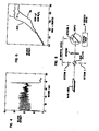
- the apparatus used to generate harmonics in the second boule, and to detect the intensity of the harmonics exiting the second boule is schematically depicted in FIG. 3. That is, as shown, light pulses incident on the second boule were emitted by a "Q"-switched Nd-doped YAG laser. The wavelength and duration of each pulse were, respectively, 1.06 ⁇ m and 300 nanoseconds. The energy in each pulse was 1 millijoule, the beam diameter was 1 millimeter, while the repetition rate was 1000 pulses per second.
- the lithium niobate boule was mounted on an adjustable table. During operation, the table permitted one of the polished windows of the boule to be kept normal to the laser beam, the polarization of the laser beam was perpendicular to the z-axis, and the boule was translated parallel to the z-axis.
- the green, harmonic light exiting the second window of the boule was separated from the infrared fundamental by a harmonic beam splitter.
- the infrared light was absorbed by a fire brick.
- the separated harmonic green light was filtered by both a glass filter and an interference filter, before being detected by a photovoltaic photodiode operated in the reverse bias mode.
- the measured harmonic intensity as a function of distance along the z-axis of the second boule, is shown in FIG. 4. As is evident, the intensity varies sinusoidally with distance.
- the relatively high frequency of the sinusoid implies a relatively large gradient in refractive index (n e ), which is consistent with the relatively large compositional gradient associated with the first boule.
- a third lithium niobate boule was drawn from a 48.00 mole percent Li2O-52.00 mole percent Nb2O5 liquid melt. This boule was cylindrical in shape, had a diameter of 1.8 cm, and a length of 9 cm.
- the refractive index homogeneity of the third boule was determined using the second optical technique, described above. In preparation for this determination, a strip-like, optically flat window, having a width of about 1 cm, was polished along the length of the boule.
- this apparatus included a TiO2 prism with a ⁇ angle (see FIG. 2) of 45 degrees and an optically flat base. During the measurement procedure, the base of the prism was placed on the polished window of the boule, at various positions along the length of the boule.
- the prism and boule were mounted in a sample holder on an adjustable table.
- the table was attached to a polar rotation stage which was driven by a stepping motor.
- the polar rotation stage rode on translator stages which positioned the prism and boule in the path of an impinging light beam.
- a microcomputer (Model Micro/PDP 11/23, sold by Digital Equipment Corporation of Boston, Massachusetts) controlled the system and determined how far and in what direction the rotator or translators moved.
- the light which impinged the prism and boule was produced by a small, single mode He-Ne laser (Model 6697, purchased from the Oriel Corporation of Stamford, Connecticut).
- the apparatus also included a beam splitter and three detectors, labeled A, B, C in FIG. 5.
- Each of the detectors was a 7 mm x 7 mm voltaic photodiode purchased from the Hamamatsu Corporation of Middlesex, New Jersey.
- detector A was used to monitor the light intensity from the laser, i.e., the beam splitter reflected a portion of the light emitted by the laser to detector A.
- detector B The light transmitted by the beam splitter to the prism, and reflected by the prism, was detected with detector B.
- the light refracted by the prism and reflected from the (ground and polished) boule window was detected with detector C.
- the break angle for the seed portion is labeled "A”
- the break angle for the tail portion is labeled "B”.
- break angles between the seed and tail portions which denotes a refractive index gradient along the length of the boule. From previous experience, it is known that this gradient is so large as to make the boule unsuitable for device fabrication.
Landscapes
- Physics & Mathematics (AREA)
- Engineering & Computer Science (AREA)
- Microelectronics & Electronic Packaging (AREA)
- General Physics & Mathematics (AREA)
- Optics & Photonics (AREA)
- Optical Integrated Circuits (AREA)
- Investigating Or Analysing Materials By Optical Means (AREA)
Applications Claiming Priority (2)
| Application Number | Priority Date | Filing Date | Title |
|---|---|---|---|
| US79308885A | 1985-10-30 | 1985-10-30 | |
| US793088 | 1985-10-30 |
Publications (2)
| Publication Number | Publication Date |
|---|---|
| EP0220935A2 true EP0220935A2 (fr) | 1987-05-06 |
| EP0220935A3 EP0220935A3 (fr) | 1989-10-25 |
Family
ID=25159058
Family Applications (1)
| Application Number | Title | Priority Date | Filing Date |
|---|---|---|---|
| EP86308215A Withdrawn EP0220935A3 (fr) | 1985-10-30 | 1986-10-22 | Méthode de fabrication de dispositifs optiques intégrés |
Country Status (3)
| Country | Link |
|---|---|
| EP (1) | EP0220935A3 (fr) |
| JP (1) | JPS62106410A (fr) |
| CA (1) | CA1284902C (fr) |
Cited By (2)
| Publication number | Priority date | Publication date | Assignee | Title |
|---|---|---|---|---|
| DE10032069A1 (de) * | 2000-07-01 | 2002-02-14 | Wolfgang Sawa | Mobiler Datenvernichter kombiniert mit vollautomatischem Presscontainer |
| WO2003038373A3 (fr) * | 2001-10-26 | 2003-10-30 | Corning Inc | Caracterisation de preformes optiques |
Family Cites Families (1)
| Publication number | Priority date | Publication date | Assignee | Title |
|---|---|---|---|---|
| US4400052A (en) * | 1981-03-19 | 1983-08-23 | Bell Telephone Laboratories, Incorporated | Method for manufacturing birefringent integrated optics devices |
-
1986
- 1986-10-22 EP EP86308215A patent/EP0220935A3/fr not_active Withdrawn
- 1986-10-29 CA CA000521707A patent/CA1284902C/fr not_active Expired - Fee Related
- 1986-10-30 JP JP25709686A patent/JPS62106410A/ja active Pending
Cited By (2)
| Publication number | Priority date | Publication date | Assignee | Title |
|---|---|---|---|---|
| DE10032069A1 (de) * | 2000-07-01 | 2002-02-14 | Wolfgang Sawa | Mobiler Datenvernichter kombiniert mit vollautomatischem Presscontainer |
| WO2003038373A3 (fr) * | 2001-10-26 | 2003-10-30 | Corning Inc | Caracterisation de preformes optiques |
Also Published As
| Publication number | Publication date |
|---|---|
| EP0220935A3 (fr) | 1989-10-25 |
| CA1284902C (fr) | 1991-06-18 |
| JPS62106410A (ja) | 1987-05-16 |
Similar Documents
| Publication | Publication Date | Title |
|---|---|---|
| Canali et al. | Structural characterization of proton exchanged LiNbO3 optical waveguides | |
| Carter et al. | Time and wavelength resolved nonlinear optical spectroscopy of a polydiacetylene in the solid state using picosecond dye laser pulses | |
| Dixon | Photoelastic properties of selected materials and their relevance for applications to acoustic light modulators and scanners | |
| US4512638A (en) | Wire grid polarizer | |
| US6641662B2 (en) | Method for fabricating ultra thin single-crystal metal oxide wave retarder plates and waveguide polarization mode converter using the same | |
| EP1015936B1 (fr) | Procede pour la polarisation de cristaux optiques | |
| Martin | Waveguide electro‐optic modulation in II‐VI compounds | |
| CA1284902C (fr) | Methode de fabrication de dispositifs optiques integres, et dispositifs ainsi produits | |
| Korkishko et al. | Proton exchanged LiNbO3 and LiTaO3 optical waveguides and integrated optic devices | |
| Fukuda et al. | Acousto‐optic properties of tellurium at 10.6 μm | |
| Haavisto | Thin-film waveguides for inertial sensors | |
| Hinkov et al. | Acoustic properties of proton exchanged LiNbO3 investigated by Brillouin scattering | |
| Biazzo | Fabrication of a lithium tantalate temperature-stabilized optical modulator | |
| Miyazawa et al. | Optical waveguiding in LiNbO3 single‐crystal film grown by the EGM technique | |
| Nightingale et al. | Monolithic Nd: YAG fiber laser | |
| Kushibiki et al. | Quantitative characterization of proton-exchanged layers in LiTaO 3 optoelectronic devices by line-focus-beam acoustic microscopy | |
| US5264959A (en) | Temperature-insensitive phase-matched optical harmonic conversion crystal | |
| Lunt et al. | Second harmonic generation for the analysis of lithium niobate substrates and boules | |
| Peterson et al. | Refractive index measurements of lithium niobate integrated optical substrates by total internal reflection | |
| Lunt et al. | Maker fringe analysis of lithium niobate integrated optical substrates | |
| Younesi et al. | Er-doping of thin-film lithium niobate on insulator using ion exchange process | |
| Cazeca et al. | Stable highly transparent nonlinear optical polymer for laser frequency doubling | |
| Vigne et al. | Optical properties of epitaxial CaxBa1-xNb2O6 thin film based rib-waveguide structure on (001) MgO for electro-optic applications | |
| JP3346176B2 (ja) | 偏光子の製造方法 | |
| Ponomarev et al. | Automatic high-precision laser scanner |
Legal Events
| Date | Code | Title | Description |
|---|---|---|---|
| PUAI | Public reference made under article 153(3) epc to a published international application that has entered the european phase |
Free format text: ORIGINAL CODE: 0009012 |
|
| AK | Designated contracting states |
Kind code of ref document: A2 Designated state(s): DE FR GB SE |
|
| PUAL | Search report despatched |
Free format text: ORIGINAL CODE: 0009013 |
|
| AK | Designated contracting states |
Kind code of ref document: A3 Designated state(s): DE FR GB SE |
|
| 17P | Request for examination filed |
Effective date: 19900410 |
|
| STAA | Information on the status of an ep patent application or granted ep patent |
Free format text: STATUS: THE APPLICATION HAS BEEN WITHDRAWN |
|
| 18W | Application withdrawn |
Withdrawal date: 19911011 |
|
| RIN1 | Information on inventor provided before grant (corrected) |
Inventor name: LUNT, SHARON RUTH Inventor name: PETERSON, GEORGE EARL |