EP0221518A2 - Grille polarisée de nettoyage pour appareil électrographique - Google Patents
Grille polarisée de nettoyage pour appareil électrographique Download PDFInfo
- Publication number
- EP0221518A2 EP0221518A2 EP86115119A EP86115119A EP0221518A2 EP 0221518 A2 EP0221518 A2 EP 0221518A2 EP 86115119 A EP86115119 A EP 86115119A EP 86115119 A EP86115119 A EP 86115119A EP 0221518 A2 EP0221518 A2 EP 0221518A2
- Authority
- EP
- European Patent Office
- Prior art keywords
- grid
- particles
- recording element
- scavenging
- image
- Prior art date
- Legal status (The legal status is an assumption and is not a legal conclusion. Google has not performed a legal analysis and makes no representation as to the accuracy of the status listed.)
- Granted
Links
Images
Classifications
-
- G—PHYSICS
- G03—PHOTOGRAPHY; CINEMATOGRAPHY; ANALOGOUS TECHNIQUES USING WAVES OTHER THAN OPTICAL WAVES; ELECTROGRAPHY; HOLOGRAPHY
- G03G—ELECTROGRAPHY; ELECTROPHOTOGRAPHY; MAGNETOGRAPHY
- G03G21/00—Arrangements not provided for by groups G03G13/00 - G03G19/00, e.g. cleaning, elimination of residual charge
- G03G21/0005—Arrangements not provided for by groups G03G13/00 - G03G19/00, e.g. cleaning, elimination of residual charge for removing solid developer or debris from the electrographic recording medium
- G03G21/0047—Arrangements not provided for by groups G03G13/00 - G03G19/00, e.g. cleaning, elimination of residual charge for removing solid developer or debris from the electrographic recording medium using electrostatic or magnetic means; Details thereof, e.g. magnetic pole arrangement of magnetic devices
-
- G—PHYSICS
- G03—PHOTOGRAPHY; CINEMATOGRAPHY; ANALOGOUS TECHNIQUES USING WAVES OTHER THAN OPTICAL WAVES; ELECTROGRAPHY; HOLOGRAPHY
- G03G—ELECTROGRAPHY; ELECTROPHOTOGRAPHY; MAGNETOGRAPHY
- G03G15/00—Apparatus for electrographic processes using a charge pattern
- G03G15/06—Apparatus for electrographic processes using a charge pattern for developing
- G03G15/08—Apparatus for electrographic processes using a charge pattern for developing using a solid developer, e.g. powder developer
- G03G15/095—Removing excess solid developer, e.g. fog preventing
Definitions
- This invention relates to apparatus for scavenging charged particles from a developed electrostatic image.
- a development electrode positioned directly opposite and in close proximity to the charge image, to a voltage intermediate that of the image and background areas constituting the charge image. For example, assuming those image areas which are to be developed with toner are charged to a level of, say, -500 volts, and the remaining areas (i.e. the backgound areas) are charged to a level of, say, -50 volts, the development electrode might be biased to -200 volts. In this manner, the positively charged toner particles will be attracted more toward the development electrode than toward the background areas of the electrostatic image.
- biasing scheme has the advantageous effect of preventing the deposition of toner particles in the background areas of the image, it has the undesirable effect of causing carrier particles to deposit on such areas and be carried out of the development zone with the developed image .
- carrier pick-up has an adverse effect on image quality and, worse yet, can produce deleterious effects in the form of scratches or scars in the surface of the recording element and other copier components, such as transfer and fusing rollers.
- a carrier scavenging apparatus comprising an electrically conductive member which is positioned downstream of the development zone in close proximity with the recording element's surface. Means are provided for DC biasing the conductive member to a voltage which renders it more attractive to the carrier particles than to the recording element. In this manner, the carrier particles are pulled from the recording element by stronger electrostatic forces.
- the latter is located relative to a magnetic brush applicator of the rotating core variety such that the particles are influenced by the rapidly changing magnetic field produced by the rotating magnetic core.
- the scavenged carrier particles are advanced by magnetic forces along the surface of the scavenging member to a position at which they return to the development sump under the force of gravity.
- An object of this invention is to provide scavenging apparatus of the type described which, upon scavenging undesired charged particles from the surface of the recording element, is less apt to become contaminated by the scavenged particles.
- a charged particle scavenging apparatus comprising a grid structure comprising a plurality of substantially parallel, non-magnetic, electrically conductive wires.
- this grid is connected to an AC power supply which is preferably DC-biased to a polarity opposite that of the charged particles to be scavenged.
- the scavenging grid is positioned in close proximity to the path of the recording element, downstream of the development zone.
- the AC grid bias functions to alternately attract the charged particles from the recording element and toward the grid, and then repel such particles from the grid itself, thereby reducing grid contamination.
- the preferred DC offset bias serves to provide a stronger electric field for scavenging particles from the recording element than for preventing grid contamination.
- the biased grid Being composed of a plurality of spaced wires, the biased grid, will allow the scavenged particles to pass (or be pulled) through the grid by the magnetic influences of a magnetic brush applicator and/or gravity to a reservoir or sump positioned directly beneath the grid.
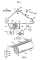
- FIG. 1 schematically illustrates an electrophotographic document copying apparatus embodying the invention.
- Such apparatus comprises an endless photoconductive recording element 10 which is trained around three rollers 12, 14 and 16, one being rotatably driven to advance the recording element in the direction of the arrow.
- recording element 10 comprises a photoconductive layer disposed on a conductive support, the latter being electrically grounded.
- the recording element receives a uniform electrostatic charge (e.g. -600 volts) at corona charging station 20. Thereafter, the uniformly charged recording element is imagewise exposed at exposure station 22 to the light and dark pattern of a document D.
- a uniform electrostatic charge e.g. -600 volts
- the light pattern corresponding to the background areas of the image, causes the uniform charge on the recording element to dissipate to, say, -50 volts
- the dark pattern corresponding to the text or graphic image which is to be developed, causes only a slight charge dissipation to, say, -500 volts.
- the resulting latent charge image then advances to developing station 30 at which an electrographic developer is applied to render the image visible.
- Development station 30 may comprise, for example, a conventional magnetic brush applicator 32 of the type comprising a non-magnetic cylindrical sleeve 34 having a magnetic core piece 36 rotatably mounted therein. Means (not shown) are provided for rotating the core piece in the direction of the arrow. Such movement of the core piece causes the magnetic developer to advance from a developer sump 38 to a development zone Z at which the developer contacts and develops the electrostatic image on the recording element. The developed image is then transferred to an image-receiving sheet S at transfer station 40 and fused to the receiver sheet at a fusing station 42. Thereafter, any residual developer on the recording element is removed by a cleaning station 44 and the recording element is recycled through the electrographic process.
- a conventional magnetic brush applicator 32 of the type comprising a non-magnetic cylindrical sleeve 34 having a magnetic core piece 36 rotatably mounted therein. Means (not shown) are provided for rotating the core piece in the direction of the arrow. Such movement of the core piece causes
- an electrographic developer is applied to the electrostatic image to render it visible at station 30.
- Such developer typically comprises a mixture of magnetic or magnetically attractive carrier particles, and pigmented thermoplastic particles called toner.
- the toner and carrier particles are triboelectrically charged to opposite polarities, the polarity of the toner particles usually being opposite the charge image.
- a development electrode bias supply 46 is shown to provide this function.
- a wire grid structure 50 is positioned downstream of the development zone Z and in close proximity to the recording element's surface.
- the grid structure is electrically connected to bias supply 52.
- the function of the bias supply is to produce an electric field which is effective to pull carrier particles from the developed image and direct such particles toward the grid, yet prevent such particles from lighting on the grid and thereby contaminating the same.
- the grid bias supply preferably comprises an AC voltage source 55 (shown in FIG. 2) having a peak-to-peak voltage of between about -00 and 800 volts, most preferably about 600 volts, and a frequency of between about 200 and 600 hertz, most preferably about 400 hertz.
- the AC signal provided by supply 55 be DC biased, e.g. by a variable DC voltage source 57.
- the polarity of the DC bias depends, of course, upon the polarity of the charged particles. Assuming the charging station 20 deposits a uniform negative charge, the toner and carrier materials are selected such that the toner and carrier particles will become charged triboelectrically to positive and negative polarities, respectively. Thus, to attract the negatively charged carrier particles toward the grid, a positive DC bias would be employed.
- the level of the DC offset supplied by voltage source 57 it should be such that, during at least a portion of the AC cycle, the grid becomes biased to the same polarity as the carrier particles, in this case negative.
- a +200 volt DC offset would produce an electric field that varies between -100 volts and +500 volts.
- the bias of the grid is +500, it is most attractive to carrier particles.
- the grid will repel the scavenged particles, allowing them to pass through the grid to the underlying developer sump without significantly contaminating the grid.
- grid structure 50 it preferably comprises between five and ten wires 60 of non-magnetic, electrically conductive, material. Such wires are electrically connected and supported in a spaced, parallel fashion by a pair of conductive supports, 62, 64. Aluminum, nickel, non-magnetic stainless steel, and copper are suitable materials for wires 60. Were the wires to be magnetic or magnetically attractive, the scavenged, magnetically attractive, carrier particles would begin to contaminate the wires, reducing the effectiveness of the bias field and making it more difficult for the scavenged particles to return to the developer sump by passage through the grid.
- the average diameter of each wire is between 0.1 and 1.0 mm and the spacing between adjacent wires is between 0.1 and 1.0 mm.
- This spacing allows the scavenged particles to pass between adjacent grid wires and thereby return to the developer sump without contaminating the grid itself.
- the positive DC bias applied to the AC bias signal does not cause any significant deposition or "plate-out" of scavenged particles on the grid wires.
- a piezoelectric transducer 70 driven by an oscillator 72 at high frequency (e.g. 400-40K Hz) may be coupled to the grid structure to mechanically vibrate the structure during the scavenging operation.
- the scavenging grid is spaced from the recording element surface between about 0.5 and 1.0 mm. A larger spacing would require a somewhat greater bias potential to produce the desired field effects. Also preferred is that the grid be closely spaced from the development zone so that the scavenged particles are within the magnetic field of the magnetic development brush and are thereby pulled through the grid by magnetic, as well as gravitational, forces.
- the advantageous technical effect of the invention is that charged particle scavenging is effected without significant contamination of the scavenging apparatus and the problems attendant such contamination.
Landscapes
- Physics & Mathematics (AREA)
- General Physics & Mathematics (AREA)
- Electrostatic Charge, Transfer And Separation In Electrography (AREA)
- Discharging, Photosensitive Material Shape In Electrophotography (AREA)
- Dry Development In Electrophotography (AREA)
Applications Claiming Priority (2)
| Application Number | Priority Date | Filing Date | Title |
|---|---|---|---|
| US06/795,007 US4647186A (en) | 1985-11-04 | 1985-11-04 | Biased scavenging grid for electrographic apparatus |
| US795007 | 1985-11-04 |
Publications (3)
| Publication Number | Publication Date |
|---|---|
| EP0221518A2 true EP0221518A2 (fr) | 1987-05-13 |
| EP0221518A3 EP0221518A3 (en) | 1987-08-26 |
| EP0221518B1 EP0221518B1 (fr) | 1989-08-23 |
Family
ID=25164368
Family Applications (1)
| Application Number | Title | Priority Date | Filing Date |
|---|---|---|---|
| EP86115119A Expired EP0221518B1 (fr) | 1985-11-04 | 1986-10-31 | Grille polarisée de nettoyage pour appareil électrographique |
Country Status (4)
| Country | Link |
|---|---|
| US (1) | US4647186A (fr) |
| EP (1) | EP0221518B1 (fr) |
| JP (1) | JPH0740167B2 (fr) |
| DE (1) | DE3665233D1 (fr) |
Cited By (1)
| Publication number | Priority date | Publication date | Assignee | Title |
|---|---|---|---|---|
| EP0366426A1 (fr) * | 1988-10-24 | 1990-05-02 | Xerox Corporation | Dispositif électrophotographique avec un ensemble de nettoyage commandé à courant alternatif |
Families Citing this family (14)
| Publication number | Priority date | Publication date | Assignee | Title |
|---|---|---|---|---|
| EP0261394B1 (fr) * | 1986-08-22 | 1993-08-11 | Canon Kabushiki Kaisha | Appareil d'enregistrement d'images |
| US5025290A (en) * | 1987-03-05 | 1991-06-18 | Savin Corporation | Pulsed voltage development electrode cleaner |
| US4837104A (en) * | 1988-06-02 | 1989-06-06 | Xerox Corporation | Scavenging field for electrostatographic printing machine |
| US4918488A (en) * | 1989-06-26 | 1990-04-17 | Eastman Kodak Company | Scavenging apparatus |
| EP0467005B1 (fr) * | 1990-07-20 | 1994-01-12 | BULL HN INFORMATION SYSTEMS ITALIA S.p.A. | Appareil de développement électrophotographique |
| US5134442A (en) * | 1990-07-26 | 1992-07-28 | Xerox Corporation | Electrode wire contamination prevention and detection |
| US5047807A (en) * | 1990-10-15 | 1991-09-10 | Eastman Kodak Company | Development apparatus having a plate scavenging device |
| US5081503A (en) * | 1991-02-04 | 1992-01-14 | Xerox Corporation | Compact magnetic bead pick-off device |
| US5184194A (en) * | 1991-10-28 | 1993-02-02 | Eastman Kodak Company | Carrier particle scavenging device |
| US5214479A (en) * | 1992-08-31 | 1993-05-25 | Xerox Corporation | BTR air cleaner with biased shims |
| US5376492A (en) * | 1993-05-20 | 1994-12-27 | Eastman Kodak Company | Method and apparatus for developing an electrostatic image using a two component developer |
| US5409791A (en) * | 1993-05-20 | 1995-04-25 | Eastman Kodak Company | Image forming method and apparatus |
| US5506372A (en) * | 1993-11-30 | 1996-04-09 | Eastman Kodak Company | Development station having a particle removing device |
| US20060027106A1 (en) * | 2003-02-10 | 2006-02-09 | Todd Craig | Apparatus and method for preparing multiple pizzas |
Family Cites Families (8)
| Publication number | Priority date | Publication date | Assignee | Title |
|---|---|---|---|---|
| JPS53116844A (en) * | 1977-03-22 | 1978-10-12 | Minolta Camera Co Ltd | Magnetic brush type developing apparatus for zerographic copying machine |
| US4190351A (en) * | 1978-11-13 | 1980-02-26 | Pitney-Bowes, Inc. | Copying machine with electromechanical scavenger assembly and process |
| US4210397A (en) * | 1978-11-13 | 1980-07-01 | Pitney Bowes Inc. | Copying machine with electromagnetic scavenger assembly and process |
| JPS5654465A (en) * | 1979-10-11 | 1981-05-14 | Minolta Camera Co Ltd | Developer removing device in copying machine |
| EP0102038A3 (fr) * | 1982-08-27 | 1984-05-16 | Kabushiki Kaisha Toshiba | Dispositif et procédé de développement |
| JPS60117275A (ja) * | 1983-11-29 | 1985-06-24 | Matsushita Electric Ind Co Ltd | トナ−除去装置 |
| JPS60117276A (ja) * | 1983-11-29 | 1985-06-24 | Matsushita Electric Ind Co Ltd | トナ−除去装置 |
| US4705387A (en) * | 1983-12-21 | 1987-11-10 | Xerox Corporation | Cleaning apparatus for charge retentive surface |
-
1985
- 1985-11-04 US US06/795,007 patent/US4647186A/en not_active Expired - Fee Related
-
1986
- 1986-10-31 DE DE8686115119T patent/DE3665233D1/de not_active Expired
- 1986-10-31 EP EP86115119A patent/EP0221518B1/fr not_active Expired
- 1986-11-04 JP JP61262595A patent/JPH0740167B2/ja not_active Expired - Lifetime
Cited By (1)
| Publication number | Priority date | Publication date | Assignee | Title |
|---|---|---|---|---|
| EP0366426A1 (fr) * | 1988-10-24 | 1990-05-02 | Xerox Corporation | Dispositif électrophotographique avec un ensemble de nettoyage commandé à courant alternatif |
Also Published As
| Publication number | Publication date |
|---|---|
| JPH0740167B2 (ja) | 1995-05-01 |
| JPS62112187A (ja) | 1987-05-23 |
| DE3665233D1 (en) | 1989-09-28 |
| EP0221518B1 (fr) | 1989-08-23 |
| EP0221518A3 (en) | 1987-08-26 |
| US4647186A (en) | 1987-03-03 |
Similar Documents
| Publication | Publication Date | Title |
|---|---|---|
| EP0334581B1 (fr) | Appareil de développement d'images électrostatiques latentes | |
| EP0221518B1 (fr) | Grille polarisée de nettoyage pour appareil électrographique | |
| US5031570A (en) | Printing apparatus and toner/developer delivery system therefor | |
| EP0426420A2 (fr) | Appareil de développement | |
| US4165393A (en) | Magnetic brush developing process for electrostatic images | |
| US4876575A (en) | Printing apparatus including apparatus and method for charging and metering toner particles | |
| US4349270A (en) | Developer removing device for copying apparatus | |
| JP3238531B2 (ja) | 画像形成装置及び方法 | |
| JPH03113474A (ja) | 電子写真式複写機 | |
| US3412710A (en) | Cleanup electrode | |
| US5206693A (en) | Development unit having an asymmetrically biased electrode wires | |
| GB2129372A (en) | Cleaning photoconductors | |
| US3662711A (en) | Development apparatus | |
| GB2074903A (en) | Developing latent images | |
| JPH0473795B2 (fr) | ||
| US5184194A (en) | Carrier particle scavenging device | |
| US3592166A (en) | Apparatus for developing electrostatic images | |
| US5504563A (en) | Scavengeless donor roll development | |
| GB2046635A (en) | Magnetic Brush Developer | |
| US3870515A (en) | Method for electrostatic paper stripping by neutralization of transfer charge | |
| US3550555A (en) | Xerographic developer separation | |
| US4105320A (en) | Transfer of conductive particles | |
| US4727823A (en) | Magnetic roll structure for transporting single component magnetic developer | |
| US4302094A (en) | Development method and apparatus | |
| US4637340A (en) | Developer metering structure |
Legal Events
| Date | Code | Title | Description |
|---|---|---|---|
| PUAI | Public reference made under article 153(3) epc to a published international application that has entered the european phase |
Free format text: ORIGINAL CODE: 0009012 |
|
| AK | Designated contracting states |
Kind code of ref document: A2 Designated state(s): DE FR GB NL |
|
| PUAL | Search report despatched |
Free format text: ORIGINAL CODE: 0009013 |
|
| AK | Designated contracting states |
Kind code of ref document: A3 Designated state(s): DE FR GB NL |
|
| 17P | Request for examination filed |
Effective date: 19880128 |
|
| 17Q | First examination report despatched |
Effective date: 19880324 |
|
| GRAA | (expected) grant |
Free format text: ORIGINAL CODE: 0009210 |
|
| AK | Designated contracting states |
Kind code of ref document: B1 Designated state(s): DE FR GB NL |
|
| REF | Corresponds to: |
Ref document number: 3665233 Country of ref document: DE Date of ref document: 19890928 |
|
| ET | Fr: translation filed | ||
| PLBE | No opposition filed within time limit |
Free format text: ORIGINAL CODE: 0009261 |
|
| STAA | Information on the status of an ep patent application or granted ep patent |
Free format text: STATUS: NO OPPOSITION FILED WITHIN TIME LIMIT |
|
| 26N | No opposition filed | ||
| PGFP | Annual fee paid to national office [announced via postgrant information from national office to epo] |
Ref country code: NL Payment date: 19931031 Year of fee payment: 8 |
|
| PG25 | Lapsed in a contracting state [announced via postgrant information from national office to epo] |
Ref country code: NL Effective date: 19950501 |
|
| NLV4 | Nl: lapsed or anulled due to non-payment of the annual fee | ||
| PGFP | Annual fee paid to national office [announced via postgrant information from national office to epo] |
Ref country code: GB Payment date: 19960916 Year of fee payment: 11 |
|
| PGFP | Annual fee paid to national office [announced via postgrant information from national office to epo] |
Ref country code: FR Payment date: 19961011 Year of fee payment: 11 |
|
| PGFP | Annual fee paid to national office [announced via postgrant information from national office to epo] |
Ref country code: DE Payment date: 19961030 Year of fee payment: 11 |
|
| PG25 | Lapsed in a contracting state [announced via postgrant information from national office to epo] |
Ref country code: GB Free format text: LAPSE BECAUSE OF NON-PAYMENT OF DUE FEES Effective date: 19971031 Ref country code: FR Free format text: THE PATENT HAS BEEN ANNULLED BY A DECISION OF A NATIONAL AUTHORITY Effective date: 19971031 |
|
| GBPC | Gb: european patent ceased through non-payment of renewal fee |
Effective date: 19971031 |
|
| PG25 | Lapsed in a contracting state [announced via postgrant information from national office to epo] |
Ref country code: DE Free format text: LAPSE BECAUSE OF NON-PAYMENT OF DUE FEES Effective date: 19980701 |
|
| REG | Reference to a national code |
Ref country code: FR Ref legal event code: ST |