EP0221624A1 - MOS-Transistor und Verfahren zur Herstellung - Google Patents
MOS-Transistor und Verfahren zur Herstellung Download PDFInfo
- Publication number
- EP0221624A1 EP0221624A1 EP86301231A EP86301231A EP0221624A1 EP 0221624 A1 EP0221624 A1 EP 0221624A1 EP 86301231 A EP86301231 A EP 86301231A EP 86301231 A EP86301231 A EP 86301231A EP 0221624 A1 EP0221624 A1 EP 0221624A1
- Authority
- EP
- European Patent Office
- Prior art keywords
- gate
- source
- process according
- trench region
- gate element
- Prior art date
- Legal status (The legal status is an assumption and is not a legal conclusion. Google has not performed a legal analysis and makes no representation as to the accuracy of the status listed.)
- Ceased
Links
Images


Classifications
-
- H—ELECTRICITY
- H10—SEMICONDUCTOR DEVICES; ELECTRIC SOLID-STATE DEVICES NOT OTHERWISE PROVIDED FOR
- H10D—INORGANIC ELECTRIC SEMICONDUCTOR DEVICES
- H10D62/00—Semiconductor bodies, or regions thereof, of devices having potential barriers
- H10D62/10—Shapes, relative sizes or dispositions of the regions of the semiconductor bodies; Shapes of the semiconductor bodies
- H10D62/17—Semiconductor regions connected to electrodes not carrying current to be rectified, amplified or switched, e.g. channel regions
- H10D62/213—Channel regions of field-effect devices
- H10D62/221—Channel regions of field-effect devices of FETs
-
- H—ELECTRICITY
- H10—SEMICONDUCTOR DEVICES; ELECTRIC SOLID-STATE DEVICES NOT OTHERWISE PROVIDED FOR
- H10D—INORGANIC ELECTRIC SEMICONDUCTOR DEVICES
- H10D30/00—Field-effect transistors [FET]
- H10D30/60—Insulated-gate field-effect transistors [IGFET]
-
- H—ELECTRICITY
- H10—SEMICONDUCTOR DEVICES; ELECTRIC SOLID-STATE DEVICES NOT OTHERWISE PROVIDED FOR
- H10D—INORGANIC ELECTRIC SEMICONDUCTOR DEVICES
- H10D64/00—Electrodes of devices having potential barriers
- H10D64/01—Manufacture or treatment
- H10D64/025—Manufacture or treatment forming recessed gates, e.g. by using local oxidation
- H10D64/027—Manufacture or treatment forming recessed gates, e.g. by using local oxidation by etching at gate locations
-
- H—ELECTRICITY
- H10—SEMICONDUCTOR DEVICES; ELECTRIC SOLID-STATE DEVICES NOT OTHERWISE PROVIDED FOR
- H10W—GENERIC PACKAGES, INTERCONNECTIONS, CONNECTORS OR OTHER CONSTRUCTIONAL DETAILS OF DEVICES COVERED BY CLASS H10
- H10W20/00—Interconnections in chips, wafers or substrates
- H10W20/01—Manufacture or treatment
- H10W20/031—Manufacture or treatment of conductive parts of the interconnections
- H10W20/056—Manufacture or treatment of conductive parts of the interconnections by filling conductive material into holes, grooves or trenches
-
- H—ELECTRICITY
- H10—SEMICONDUCTOR DEVICES; ELECTRIC SOLID-STATE DEVICES NOT OTHERWISE PROVIDED FOR
- H10W—GENERIC PACKAGES, INTERCONNECTIONS, CONNECTORS OR OTHER CONSTRUCTIONAL DETAILS OF DEVICES COVERED BY CLASS H10
- H10W20/00—Interconnections in chips, wafers or substrates
- H10W20/40—Interconnections external to wafers or substrates, e.g. back-end-of-line [BEOL] metallisations or vias connecting to gate electrodes
- H10W20/41—Interconnections external to wafers or substrates, e.g. back-end-of-line [BEOL] metallisations or vias connecting to gate electrodes characterised by their conductive parts
- H10W20/44—Conductive materials thereof
- H10W20/4451—Semiconductor materials, e.g. polysilicon
-
- Y—GENERAL TAGGING OF NEW TECHNOLOGICAL DEVELOPMENTS; GENERAL TAGGING OF CROSS-SECTIONAL TECHNOLOGIES SPANNING OVER SEVERAL SECTIONS OF THE IPC; TECHNICAL SUBJECTS COVERED BY FORMER USPC CROSS-REFERENCE ART COLLECTIONS [XRACs] AND DIGESTS
- Y10—TECHNICAL SUBJECTS COVERED BY FORMER USPC
- Y10S—TECHNICAL SUBJECTS COVERED BY FORMER USPC CROSS-REFERENCE ART COLLECTIONS [XRACs] AND DIGESTS
- Y10S148/00—Metal treatment
- Y10S148/082—Ion implantation FETs/COMs
Definitions
- ion implantation is used to heavily dope the source and drain regions to a shallow junction depth.
- the implanted shallow junction is deficient because of problems with the corner profile.
- a process for manufacturing an MOS transistor comprises:-
- an MOS transistor comprises a monocrystalline semiconductor substrate having a trench region therein, said trench region being covered along its bottom and vertical surfaces by a gate insulation layer; a gate element juxtaposed to said gate insulation layer composed of semiconductor material and substantially filling the trench region in said semiconductor substrate; source and drain elements having interposed therebetween said trench region and being contiguous to the vertical portions of said gate insulation layers so as to provide insulation between said gate element and each of said source and drain elements; said source and drain elements and said gate element being in substantially the same plane and doped simultaneously with an n-type (or p-type) impurity.
- the present invention describes an MOS transistor having a trench in the channel region.
- the now ancient U.S. patent 3,805,129 shows the gate of a field effect transistor deposited on the bottom of a trench.
- this reference does not show, among other things, a gate in the same plane as the source and drain regions, or doping to simultaneously form a gate, source and drain region.
- the invention provides a transistor having good junction reliability, suitable for a high density integrated circuit. Buried contacts formed by the method have low sheet resistance compared with those formed using conventional methods. The short channel effect observed in conventional MOS transistors is reduced.
- the trench structure can be etched by reactive ion etching as described in U.S. patent Nos.4,139,442; 4,356,211; and 4,477,310.
- the MOS structure having the trench structure of the invention will have the advantage of less small-geometry effects because there is less overlapping charge between the depleted channel and the depleted source (and/or drain) regions.
- Another advantage of the present invention is the ease of self-alignment of the heavily doped source and drain, and the preferred polycrystalline silicon (polysilicon) gate electrode.
- This self-alignment also provides self-alignment of the contact between the conducting polysilicon lines and the source and drain regions.
- the self-alignment makes the dimension loss much less with the same feature size when a given photolithographic technique is performed.
- the third advantage is that the shortcomings of shallow junction implantation due to the sharp concentration profile on junction corners in the conventional planar MOS structure is overcome. Deeper junction depth in source and drain doping is acceptable, thereby giving a better junction profile on the junction corners.
- Preferred features of the invention are a method of fabrication of a trench channel MOS transistor in which oxidation is performed to remedy the curvature problem and to ensure meeting the specification on field strength of oxide breakdown on the trench corners, and connection of the interconnection metal lines with conducting polysilicon on the top of field oxide regions.
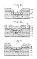
- a dielectric etching mask is formed on a substrate 10, made of a p-type monocrystalline semiconductor material such as silicon and having a resistivity of about 25 ohm-cm at (100) orientation.
- the etching mask depicted in Figures 2A and 2B is thermally grown on the surface of the substrate in an atmosphere of steam at 1100°C for 90 minutes, resulting in a thickness of about 8,000 angstroms.
- a photoresist layer 4 is coated over the top of the oxide layer 2, exposed to a light pattern and developed to form an etching mask by conventional photolithographic techniques.
- the photoresist mask thus formed has a mask opening 18 through the photoresist layer 4 to the upper surface of the oxide layer 2.
- a portion of the silicon dioxide layer 2 is removed beneath the opening 18 by etching through the oxide layer in a conventional manner, such as by reactive ion etching.
- the etched silicon dioxide layer 2 with opening 18 therethrough serves as an oxide mask for etching the substrate 10.
- Fig. 2B shows the next steps of the process.
- the photoresist layer 4 is completely removed and the substrate is etched through mask opening 7 to form a trench 20 in alignment with the mask opening.
- the trench is about 2 microns wide and 0.8 micron deep.
- Reactive ion etching using a plasma gas of either Ar + NH3 or CCl4 + Cl2 gas is used in order to anisotropically etch the substrate 10. Reactive ion etching is described in U.S. Pat. No. 4,356,211 of Riseman.
- the silicon dioxide layer 2 contaminated with impurities, is removed by etching after the trench 20 is formed.
- dielectric isolation regions are formed to separate the transistors from one another.
- a layer 6 of silicon dioxide about 500 angstroms thick is thermally grown on the surface of the substrate 10, including the vertical and bottom surfaces of the trench 20.
- the oxide layer 6 is produced by heating the semiconductor device in oxygen at a temperature of 1000°C for 50 minutes.
- a layer 8 of silicon nitride about 1500 angstroms is deposited using low pressure chemical vapor deposition (LPCVD) on the top surface of the silicon dioxide layer 6.
- LPCVD low pressure chemical vapor deposition
- a photoresist layer 12 is deposited and photolithographical processed to produce an etch mask over the silicon nitride layer 8 and to provide an etching mask over the trench 20.
- the silicon nitride layer 8 is then etched by reactive ion etching in a conventional manner with CH4 + O2 gas using a D. C. voltage field and an A.C. voltage radio frequency field to produce a plasma of etching gas ions. This process removes the portion of the silicon nitride layer in alignment with the etching mask.
- a field region 16 of p-type material is implanted by ion bombardment of boron impurity atoms through the opened area into the substrate 10. The structure at this stage is shown in Fig. 2C. Thereafter, the photoresist layer 12 is removed and, as shown in Fig.
- the portions of the silicon dioxide layer 6 above the field region 16 are increased in thickness to about 8000 angstroms by thermal growth to form the oxide regions 14.
- the thermal growth is effected by heating in steam at 1000°C for approximately 5 hours. These regions provide the dielectric isolation. Undesirable "bird's beak" shaped ends of tapered thickness are formed on oxide regions 14 due to lateral diffusion of the oxygen atoms from the oxide layers 6.
- the silicon nitride layer 8 is removed by etching in hot phosphoric acid at approximately 180°C and the silicon dioxide layers 6 removed by wet chemical etching using an aqueous solution of buffered hydrogen fluoride, HF (aq.) + NH4+ (aq.) + F (aq.), in order to eliminate the contaminated silicon dioxide.
- Fig. 2F shows a gate oxidation layer 22 of silicon dioxide (about 300 angstroms) formed by thermal growth oxidation over the trench region 20 and the region 18 of the substrate 10.
- This gate oxidation layer 22 is formed by heating the silicon in oxygen at a temperature of 920°C.
- a p-channel region 40 is formd by ion bombardment implanting of boron or other p type impurities into the upper surface of the substrate 12 throughout the wafer.
- the p-channel region 40 merges with the field region 16 also of p-type material.
- a layer of polycrystalline silicon 24, about 1.2 microns, is deposited by chemical vapor deposition on the upper surface of the oxide layer 22.
- the deposited polycrystalline silicon layer 24 refills the trench region 20 and planarizes the upper surface in region 42.
- the polycrystalline silicon layer 24 is removed from the upper surface of the substrate 10 by reactive ion etching down to the surface of the thin silicon dioxide layer 22.
- the portion of the thin silicon dioxide layer 22 atop of the region 18 is removed chemically using an aqueous solution of buffered hydrogen fluoride.
- the wafer is doped by heating in a "thermal drive" step using phosphorus or other n-type impurity to provide a n+ polycrystalline silicon gate element 24 and the n+ silicon regions 26, the latter serving as the source and drain regions.
- the n+ silicon regions 26 have n+ characteristics because the dopant concentration of p-type impurity previously implanted into this region was controlled so that its concentration would be much lower compared to the amount of n-type dopant added.
- a photoresist layer 44 is deposited over the polycrystalline silicon layer 28 and a mask is formed from such photoresist layer by conventional photolithographic techniques. The polycrystalline silicon layer is etched away in those areas not covered by the photoresist mask, leaving the so-called "buried contact" interconnection lines of n+ polycrystalline silicon 28. The resulting structure is shown in Fig. 2K.
- a layer of silicon dioxide 30 (about 1000 angstroms) is formed on the top surface by thermal growth in oxygen at the temperature of 920°C and a layer of silica glass 32 (about 8000 angstroms doped with the phosphorus impurity of about 3%) is deposited using chemical vapor deposition (CVD).
- CVD chemical vapor deposition
- Other good dielectric insulators can be deposited at lower temperatures ( ⁇ 700°C) to form layer 32.
- a photoresist layer 34 is coated over the silica glass layer 32 and a mask is formed from such photoresist layer by conventional photolithographic techniques.
- the openings 38 are formed by either a conventional wet-chemical-etching using buffered hydrogen fluoride solution or reactive ion etching. The resulting structure is shown in Fig. 2L.
- the photoresist layer 34 is removed and a metal contact 36, shown in Fig. 2M, is deposited by sputtering through the contact openings 38 into electrical contact with the conductive polycrystalline silicon layers 28.
- the contacts 36 may be made of a pure aluminum, or an alloy of 98.5% aluminum and 1.5 % silicon.
- Photoresist etching of the metal layer 36 provides three contacts which are spaced apart for electrical insulation; two of them are connected through the conductive polycrystalline silicon 28 to the source and drain regions 26 and one of them (not shown) is connected through a conductive polycrystalline silicon (not shown) to the gate element 24.
- a completed trench channel MOS transistor is shown in Fig. 2M, including the refilled polycrystalline silicon gate element and the buried contacts of n+ polycrystalline silicon to n+ source and drain regions.
- the trench channel MOS transistor of Fig. 2M also includes a trench channel region in the trench 20 having a silicon dioxide layer 22 on the inner surface of such trench and a filling 24 of n+ polycrystalline silicon deposited over such oxide layer.
- the source and drain elements 26 and gate element 24 of the trench transistor are connected to n+ polycrystalline silicon lines 28.
- the dielectric isolation 14 with the field implanted regions 16 are used to separate such trench transistor from other devices on the wafer.
Landscapes
- Insulated Gate Type Field-Effect Transistor (AREA)
- Electrodes Of Semiconductors (AREA)
Applications Claiming Priority (2)
| Application Number | Priority Date | Filing Date | Title |
|---|---|---|---|
| US06/760,129 US4685196A (en) | 1985-07-29 | 1985-07-29 | Method for making planar FET having gate, source and drain in the same plane |
| US760129 | 1985-07-29 |
Publications (1)
| Publication Number | Publication Date |
|---|---|
| EP0221624A1 true EP0221624A1 (de) | 1987-05-13 |
Family
ID=25058180
Family Applications (1)
| Application Number | Title | Priority Date | Filing Date |
|---|---|---|---|
| EP86301231A Ceased EP0221624A1 (de) | 1985-07-29 | 1986-02-21 | MOS-Transistor und Verfahren zur Herstellung |
Country Status (3)
| Country | Link |
|---|---|
| US (1) | US4685196A (de) |
| EP (1) | EP0221624A1 (de) |
| JP (1) | JPS6226863A (de) |
Cited By (1)
| Publication number | Priority date | Publication date | Assignee | Title |
|---|---|---|---|---|
| EP0299505A3 (en) * | 1987-07-16 | 1990-01-24 | Kabushiki Kaisha Toshiba | Semiconductor device and manufacturing method thereof |
Families Citing this family (25)
| Publication number | Priority date | Publication date | Assignee | Title |
|---|---|---|---|---|
| FR2582445B1 (fr) * | 1985-05-21 | 1988-04-08 | Efcis | Procede de fabrication de transistors mos a electrodes de siliciure metallique |
| JP2646547B2 (ja) * | 1987-03-19 | 1997-08-27 | 日本電気株式会社 | 半導体装置の製造方法 |
| JPH01151268A (ja) * | 1987-12-08 | 1989-06-14 | Mitsubishi Electric Corp | 半導体装置の製造方法 |
| FR2625044B1 (fr) * | 1987-12-18 | 1990-08-31 | Commissariat Energie Atomique | Transistor mos a extremite d'interface dielectrique de grille/substrat relevee et procede de fabrication de ce transistor |
| US4900693A (en) * | 1987-12-21 | 1990-02-13 | United Technologies | Process for making polysilicon field plate with improved suppression of parasitic transistors |
| US5198378A (en) * | 1988-10-31 | 1993-03-30 | Texas Instruments Incorporated | Process of fabricating elevated source/drain transistor |
| US4895520A (en) * | 1989-02-02 | 1990-01-23 | Standard Microsystems Corporation | Method of fabricating a submicron silicon gate MOSFETg21 which has a self-aligned threshold implant |
| US5108937A (en) * | 1991-02-01 | 1992-04-28 | Taiwan Semiconductor Manufacturing Company | Method of making a recessed gate MOSFET device structure |
| JP2603886B2 (ja) * | 1991-05-09 | 1997-04-23 | 日本電信電話株式会社 | 薄層soi型絶縁ゲート型電界効果トランジスタの製造方法 |
| US5342796A (en) * | 1991-05-28 | 1994-08-30 | Sharp Kabushiki Kaisha | Method for controlling gate size for semiconduction process |
| JPH0677480A (ja) * | 1992-08-24 | 1994-03-18 | Hitachi Ltd | 半導体装置 |
| US5620911A (en) * | 1993-12-31 | 1997-04-15 | Hyundai Electronics Industries Co., Ltd. | Method for fabricating a metal field effect transistor having a recessed gate |
| US5814544A (en) * | 1994-07-14 | 1998-09-29 | Vlsi Technology, Inc. | Forming a MOS transistor with a recessed channel |
| JP4077529B2 (ja) * | 1996-05-22 | 2008-04-16 | フェアチャイルドコリア半導体株式会社 | トレンチ拡散mosトランジスタの製造方法 |
| US6358817B1 (en) * | 1997-12-09 | 2002-03-19 | Matsushita Electric Industrial Co., Ltd. | Semiconductor storage unit and method of manufacturing the same |
| TW396460B (en) * | 1998-01-09 | 2000-07-01 | United Microelectronics Corp | Metal oxide semiconductor transistor structure and its manufacturing method |
| US5998835A (en) | 1998-02-17 | 1999-12-07 | International Business Machines Corporation | High performance MOSFET device with raised source and drain |
| US6614074B2 (en) | 1998-06-05 | 2003-09-02 | International Business Machines Corporation | Grooved planar DRAM transfer device using buried pocket |
| US6465842B2 (en) | 1998-06-25 | 2002-10-15 | Kabushiki Kaisha Toshiba | MIS semiconductor device and method of fabricating the same |
| US6110767A (en) * | 1998-07-16 | 2000-08-29 | Vanguard International Semiconductor Corporation | Reversed MOS |
| US6121651A (en) * | 1998-07-30 | 2000-09-19 | International Business Machines Corporation | Dram cell with three-sided-gate transfer device |
| KR100485176B1 (ko) * | 2003-01-30 | 2005-04-22 | 동부아남반도체 주식회사 | 모스 트랜지스터의 제조 방법 |
| JP2005354023A (ja) * | 2004-05-14 | 2005-12-22 | Seiko Epson Corp | 半導体装置および半導体装置の製造方法 |
| KR100620442B1 (ko) * | 2004-06-08 | 2006-09-08 | 삼성전자주식회사 | 반도체 장치의 제조 방법 |
| WO2026022653A1 (en) * | 2024-07-23 | 2026-01-29 | Zinite Corporation | Stackable and self-aligned tft structures |
Citations (1)
| Publication number | Priority date | Publication date | Assignee | Title |
|---|---|---|---|---|
| FR2526586A1 (fr) * | 1982-05-04 | 1983-11-10 | Efcis | Transistor a effet de champ a grille profonde et procede de fabrication |
Family Cites Families (9)
| Publication number | Priority date | Publication date | Assignee | Title |
|---|---|---|---|---|
| US3764413A (en) * | 1970-11-25 | 1973-10-09 | Nippon Electric Co | Method of producing insulated gate field effect transistors |
| US4441941A (en) * | 1980-03-06 | 1984-04-10 | Tokyo Shibaura Denki Kabushiki Kaisha | Method for manufacturing a semiconductor device employing element isolation using insulating materials |
| US4356211A (en) * | 1980-12-19 | 1982-10-26 | International Business Machines Corporation | Forming air-dielectric isolation regions in a monocrystalline silicon substrate by differential oxidation of polysilicon |
| US4444605A (en) * | 1982-08-27 | 1984-04-24 | Texas Instruments Incorporated | Planar field oxide for semiconductor devices |
| JPS59161073A (ja) * | 1983-03-04 | 1984-09-11 | Hitachi Ltd | 半導体装置 |
| JPS59161069A (ja) * | 1983-03-04 | 1984-09-11 | Oki Electric Ind Co Ltd | Mos型半導体装置の製造方法 |
| US4477310A (en) * | 1983-08-12 | 1984-10-16 | Tektronix, Inc. | Process for manufacturing MOS integrated circuit with improved method of forming refractory metal silicide areas |
| US4609413A (en) * | 1983-11-18 | 1986-09-02 | Motorola, Inc. | Method for manufacturing and epitaxially isolated semiconductor utilizing etch and refill technique |
| US4554728A (en) * | 1984-06-27 | 1985-11-26 | International Business Machines Corporation | Simplified planarization process for polysilicon filled trenches |
-
1985
- 1985-07-29 US US06/760,129 patent/US4685196A/en not_active Expired - Fee Related
-
1986
- 1986-02-21 EP EP86301231A patent/EP0221624A1/de not_active Ceased
- 1986-04-04 JP JP61078056A patent/JPS6226863A/ja active Pending
Patent Citations (1)
| Publication number | Priority date | Publication date | Assignee | Title |
|---|---|---|---|---|
| FR2526586A1 (fr) * | 1982-05-04 | 1983-11-10 | Efcis | Transistor a effet de champ a grille profonde et procede de fabrication |
Non-Patent Citations (2)
| Title |
|---|
| JAPANESE JOURNAL OF APPLIED PHYSICS, vol. 16, supplement 16-1, 1977, pages 179-183, Tokyo, JP; S. NISHIMATSU et al.: "Grooved gate MOSFET" * |
| PATENT ABSTRACTS OF JAPAN, vol. 6, no. 12 (E-91)[890], 23rd January 1982; & JP - A - 56 133 869 (OKI DENKI) 20-10-1981 * |
Cited By (3)
| Publication number | Priority date | Publication date | Assignee | Title |
|---|---|---|---|---|
| EP0299505A3 (en) * | 1987-07-16 | 1990-01-24 | Kabushiki Kaisha Toshiba | Semiconductor device and manufacturing method thereof |
| US4952993A (en) * | 1987-07-16 | 1990-08-28 | Kabushiki Kaisha Toshiba | Semiconductor device and manufacturing method thereof |
| US5093273A (en) * | 1987-07-16 | 1992-03-03 | Kabushiki Kaisha Toshiba | Method of manufacturing a semiconductor device |
Also Published As
| Publication number | Publication date |
|---|---|
| JPS6226863A (ja) | 1987-02-04 |
| US4685196A (en) | 1987-08-11 |
Similar Documents
| Publication | Publication Date | Title |
|---|---|---|
| US4685196A (en) | Method for making planar FET having gate, source and drain in the same plane | |
| EP0244366B1 (de) | Selbstausrichtendes Verfahren zur Herstellung kleiner DMOS-Zellen und durch dieses Verfahren erhaltene MOS-Bauelemente | |
| EP0139371B1 (de) | Verfahren zum Herstellen integrierter MOS-Schaltungen unter Verwendung eines Verfahrens zur Bildung von Oberflächenbereichen aus Siliciden hochschmelzender Metalle | |
| US5369045A (en) | Method for forming a self-aligned lateral DMOS transistor | |
| EP0088922B1 (de) | Verfahren zum Herstellen von Elektroden und Verdrahtungsstreifen auf einer Halbleiteranordnung | |
| US4682405A (en) | Methods for forming lateral and vertical DMOS transistors | |
| EP0138978B1 (de) | Verfahren zum herstellen einer halbleiteranordnung mit kleinen abmessungen | |
| US6518155B1 (en) | Device structure and method for reducing silicide encroachment | |
| US4716126A (en) | Fabrication of double diffused metal oxide semiconductor transistor | |
| KR970000535B1 (ko) | Mos 전계효과 트랜지스터 및 그 회로 제조방법 | |
| US5349224A (en) | Integrable MOS and IGBT devices having trench gate structure | |
| US4810665A (en) | Semiconductor device and method of fabrication | |
| US5283456A (en) | Vertical gate transistor with low temperature epitaxial channel | |
| US20040014276A1 (en) | Method of making a semiconductor transistor | |
| KR100289474B1 (ko) | Dmos 트랜지스터를 제조하기 위한 방법 | |
| US4486266A (en) | Integrated circuit method | |
| US4546375A (en) | Vertical IGFET with internal gate and method for making same | |
| US5969393A (en) | Semiconductor device and method of manufacture of the same | |
| US5646435A (en) | Method for fabricating CMOS field effect transistors having sub-quarter micrometer channel lengths with improved short channel effect characteristics | |
| WO1998012741A1 (en) | Short channel non-self aligned vmos field effect transistor | |
| EP0227894A2 (de) | Vertikaler DMOS-Transistor von hoher Packungsdichte | |
| US5525535A (en) | Method for making doped well and field regions on semiconductor substrates for field effect transistors using liquid phase deposition of oxides | |
| US4948744A (en) | Process of fabricating a MISFET | |
| US6011272A (en) | Silicided shallow junction formation and structure with high and low breakdown voltages | |
| US6087248A (en) | Method of forming a transistor having thin doped semiconductor gate |
Legal Events
| Date | Code | Title | Description |
|---|---|---|---|
| PUAI | Public reference made under article 153(3) epc to a published international application that has entered the european phase |
Free format text: ORIGINAL CODE: 0009012 |
|
| AK | Designated contracting states |
Kind code of ref document: A1 Designated state(s): AT BE CH DE FR GB IT LI LU NL SE |
|
| 17P | Request for examination filed |
Effective date: 19871027 |
|
| 17Q | First examination report despatched |
Effective date: 19900625 |
|
| STAA | Information on the status of an ep patent application or granted ep patent |
Free format text: STATUS: THE APPLICATION HAS BEEN REFUSED |
|
| 18R | Application refused |
Effective date: 19920413 |
|
| RIN1 | Information on inventor provided before grant (corrected) |
Inventor name: LEE, MING-KWANG |