EP0221638B1 - Palpeur capacitif en champ de dispersion et procédé - Google Patents
Palpeur capacitif en champ de dispersion et procédé Download PDFInfo
- Publication number
- EP0221638B1 EP0221638B1 EP86306192A EP86306192A EP0221638B1 EP 0221638 B1 EP0221638 B1 EP 0221638B1 EP 86306192 A EP86306192 A EP 86306192A EP 86306192 A EP86306192 A EP 86306192A EP 0221638 B1 EP0221638 B1 EP 0221638B1
- Authority
- EP
- European Patent Office
- Prior art keywords
- probe
- plate element
- capacitance
- electrode
- fringe field
- Prior art date
- Legal status (The legal status is an assumption and is not a legal conclusion. Google has not performed a legal analysis and makes no representation as to the accuracy of the status listed.)
- Expired - Lifetime
Links
- 238000000034 method Methods 0.000 title claims description 41
- 239000000523 sample Substances 0.000 claims abstract description 94
- 238000005259 measurement Methods 0.000 claims abstract description 66
- 238000001514 detection method Methods 0.000 claims description 13
- 229910010293 ceramic material Inorganic materials 0.000 claims description 7
- 230000003213 activating effect Effects 0.000 claims 2
- 238000012876 topography Methods 0.000 abstract description 8
- 239000003990 capacitor Substances 0.000 description 16
- 238000007689 inspection Methods 0.000 description 14
- 238000004519 manufacturing process Methods 0.000 description 10
- 230000004044 response Effects 0.000 description 10
- 230000005684 electric field Effects 0.000 description 8
- 230000035945 sensitivity Effects 0.000 description 8
- 230000007423 decrease Effects 0.000 description 7
- 239000004020 conductor Substances 0.000 description 6
- 230000003287 optical effect Effects 0.000 description 5
- 239000006091 Macor Substances 0.000 description 4
- 239000000463 material Substances 0.000 description 4
- 229910052751 metal Inorganic materials 0.000 description 4
- 239000002184 metal Substances 0.000 description 4
- 238000001228 spectrum Methods 0.000 description 4
- 230000003746 surface roughness Effects 0.000 description 4
- OKTJSMMVPCPJKN-UHFFFAOYSA-N Carbon Chemical compound [C] OKTJSMMVPCPJKN-UHFFFAOYSA-N 0.000 description 3
- 241001422033 Thestylus Species 0.000 description 3
- 239000000919 ceramic Substances 0.000 description 3
- 230000008859 change Effects 0.000 description 3
- 239000002131 composite material Substances 0.000 description 3
- 238000011109 contamination Methods 0.000 description 3
- 238000010586 diagram Methods 0.000 description 3
- 229910002804 graphite Inorganic materials 0.000 description 3
- 239000010439 graphite Substances 0.000 description 3
- 230000008569 process Effects 0.000 description 3
- 230000003068 static effect Effects 0.000 description 3
- 241000935974 Paralichthys dentatus Species 0.000 description 2
- 238000004458 analytical method Methods 0.000 description 2
- 230000008901 benefit Effects 0.000 description 2
- 238000011088 calibration curve Methods 0.000 description 2
- 238000010276 construction Methods 0.000 description 2
- 230000007547 defect Effects 0.000 description 2
- 238000005137 deposition process Methods 0.000 description 2
- 238000005553 drilling Methods 0.000 description 2
- 238000003780 insertion Methods 0.000 description 2
- 230000037431 insertion Effects 0.000 description 2
- 238000012544 monitoring process Methods 0.000 description 2
- 230000010355 oscillation Effects 0.000 description 2
- 238000004886 process control Methods 0.000 description 2
- 238000004439 roughness measurement Methods 0.000 description 2
- 238000000926 separation method Methods 0.000 description 2
- 229910052709 silver Inorganic materials 0.000 description 2
- 239000004332 silver Substances 0.000 description 2
- 229910000838 Al alloy Inorganic materials 0.000 description 1
- VYZAMTAEIAYCRO-UHFFFAOYSA-N Chromium Chemical compound [Cr] VYZAMTAEIAYCRO-UHFFFAOYSA-N 0.000 description 1
- 239000004593 Epoxy Substances 0.000 description 1
- VVQNEPGJFQJSBK-UHFFFAOYSA-N Methyl methacrylate Chemical compound COC(=O)C(C)=C VVQNEPGJFQJSBK-UHFFFAOYSA-N 0.000 description 1
- 229920005372 Plexiglas® Polymers 0.000 description 1
- 230000004913 activation Effects 0.000 description 1
- 238000013459 approach Methods 0.000 description 1
- 238000003491 array Methods 0.000 description 1
- 229910052804 chromium Inorganic materials 0.000 description 1
- 239000011651 chromium Substances 0.000 description 1
- 239000011248 coating agent Substances 0.000 description 1
- 238000000576 coating method Methods 0.000 description 1
- 238000007796 conventional method Methods 0.000 description 1
- 230000007797 corrosion Effects 0.000 description 1
- 238000005260 corrosion Methods 0.000 description 1
- 238000006880 cross-coupling reaction Methods 0.000 description 1
- 239000002173 cutting fluid Substances 0.000 description 1
- 230000003247 decreasing effect Effects 0.000 description 1
- 238000013461 design Methods 0.000 description 1
- 238000006073 displacement reaction Methods 0.000 description 1
- 230000000694 effects Effects 0.000 description 1
- 239000007772 electrode material Substances 0.000 description 1
- 238000004070 electrodeposition Methods 0.000 description 1
- 230000007613 environmental effect Effects 0.000 description 1
- 229920006335 epoxy glue Polymers 0.000 description 1
- 239000003822 epoxy resin Substances 0.000 description 1
- 239000000835 fiber Substances 0.000 description 1
- 238000001914 filtration Methods 0.000 description 1
- 239000006112 glass ceramic composition Substances 0.000 description 1
- 238000003384 imaging method Methods 0.000 description 1
- 239000011810 insulating material Substances 0.000 description 1
- 238000012886 linear function Methods 0.000 description 1
- 238000003754 machining Methods 0.000 description 1
- 238000000691 measurement method Methods 0.000 description 1
- 239000002923 metal particle Substances 0.000 description 1
- 238000001465 metallisation Methods 0.000 description 1
- 238000003801 milling Methods 0.000 description 1
- 229920000647 polyepoxide Polymers 0.000 description 1
- 238000003908 quality control method Methods 0.000 description 1
- 238000005316 response function Methods 0.000 description 1
- 238000007493 shaping process Methods 0.000 description 1
- 239000010935 stainless steel Substances 0.000 description 1
- 229910001220 stainless steel Inorganic materials 0.000 description 1
- 238000004441 surface measurement Methods 0.000 description 1
- 239000000725 suspension Substances 0.000 description 1
- 238000012360 testing method Methods 0.000 description 1
- 238000002207 thermal evaporation Methods 0.000 description 1
- 238000007514 turning Methods 0.000 description 1
Images


Classifications
-
- G—PHYSICS
- G01—MEASURING; TESTING
- G01B—MEASURING LENGTH, THICKNESS OR SIMILAR LINEAR DIMENSIONS; MEASURING ANGLES; MEASURING AREAS; MEASURING IRREGULARITIES OF SURFACES OR CONTOURS
- G01B7/00—Measuring arrangements characterised by the use of electric or magnetic techniques
- G01B7/12—Measuring arrangements characterised by the use of electric or magnetic techniques for measuring diameters
-
- G—PHYSICS
- G01—MEASURING; TESTING
- G01B—MEASURING LENGTH, THICKNESS OR SIMILAR LINEAR DIMENSIONS; MEASURING ANGLES; MEASURING AREAS; MEASURING IRREGULARITIES OF SURFACES OR CONTOURS
- G01B7/00—Measuring arrangements characterised by the use of electric or magnetic techniques
- G01B7/02—Measuring arrangements characterised by the use of electric or magnetic techniques for measuring length, width or thickness
- G01B7/023—Measuring arrangements characterised by the use of electric or magnetic techniques for measuring length, width or thickness for measuring distance between sensor and object
-
- G—PHYSICS
- G01—MEASURING; TESTING
- G01B—MEASURING LENGTH, THICKNESS OR SIMILAR LINEAR DIMENSIONS; MEASURING ANGLES; MEASURING AREAS; MEASURING IRREGULARITIES OF SURFACES OR CONTOURS
- G01B7/00—Measuring arrangements characterised by the use of electric or magnetic techniques
- G01B7/28—Measuring arrangements characterised by the use of electric or magnetic techniques for measuring contours or curvatures
Definitions
- the present invention relates to an apparatus and method for measuring the distance between a probe and the surface of a body.
- Applications of the invention include the measurement of surface profile, hole geometry and surface topography.
- One important class of inspection procedures consists of dimensional measurements, for example measurement of the finish or geometry required in manufacturing of a surface. Finish refers to the roughness or small scale height variations of a surface, whereas geometry refers to the macroscopic characteristics of the surface. In-process inspection procedures based upon the measurement of such dimensions must be designed to survive in a comparatively harsh environment without sacrificing dynamic range, accuracy, or speed.
- the inspection and quality control of drilled holes is of a special concern to certain industries, such as the aircraft industry.
- the diameter, finish and shape of holes drilled for fasteners in aircraft manufacturing must meet exceptionally high tolerances, because the fit of the fastener in the hole is critical to the strength and fatigue life of the joint. This is particularly true where the components are high-strength aluminum alloys, which are often fairly brittle and therefore notch sensitive.
- a commercial jet aircraft may contain a million drilled holes, and the inspection of all such holes by conventional techniques is impractical.
- inspection procedures typically rely on statistical inference based upon the inspection of a certain fraction of the holes. However, even such partial inspection is time consuming, and depends to a considerable extent upon the skill and experience of the inspector.
- Prior surface finish measurement techniques may be divided into two classes: (1) those which measure or infer only average roughness and, (2) those which record the surface profile, i.e., the local height of the surface as a function of distance along the surface.
- the surface profile provides substantially more information than average roughness alone.
- Higher order statistics such as skewness, kurtosis, and surface spectra can be computed from the profile record, but not from the value of the average roughness.
- profile measurements are usually necessary for reliable detection of individual cracks and tool gouges. The average roughness measurement from a surface containing an isolated surface defect is often indistinguishable from that of a surface containing uniform roughness of equivalent value.
- the stylus-type profilometer is the device most commonly used to measure profile and average roughness.
- the stylus tip must mechanically follow the vertical height variations as the stylus is moved across the surface, and scanning speeds must therefore be relatively slow.
- the stylus tip suspension is fragile and is easily damaged.
- optical surface measurement techniques have been developed. These are noncontacting systems and have potentially high scanning speeds. Some are capable of profile measurements, as well as average roughness estimates. Disadvantages of these techniques are the potential complexity of the optical apparatus (light source, optics, alignment devices, detectors), and the possibility of errors due to contamination by cutting fluids and metal particles.
- a pneumatic technique has also been used to measure surface finish.
- a close-fitting sensor is placed against a machined surface and air is allowed to flow between the sensor and the surface.
- the pressure required to sustain a fixed flow rate is related to the characteristics of the surface finish. This method is limited to the measurement of average surface roughness, and has comparatively poor time response.
- CMOS complementary metal-oxide-semiconductor
- capacitance generated between these two conductors is inversely proportional to the average roughness of the surface.
- the sensor is rugged and the method is well suited to the manufacturing environment. However, only average roughness can be measured.
- GB-A-2 150 304 (Matey) describes a device referred to as a scanning capacitance microscope. The features of this device and the method of its operation are set out in the preamble of the independent claims.
- the scanning capacitance microscope uses a probe carrying a shaped plate electrode element intended to be scanned over the surface of a video disc which has been made conductive by the application of a conformal metal coating.
- the probe is described as a stylus and the edge of the plate electrode facing the surface shown in the embodiment is pointed. It is intended that the electrode should move up and down as the probe or stylus moves along the grooves of the video disc in order to measure the topography of the disc surface. It is appreciated that the capacitance between the electrode and the surface will vary as a function of the topography.
- the most common hole geometry measurement system employed in industry is the air gauge.
- An air gauge consists of a close tolerance rod inserted inside the hole to be measured. Compressed air is then allowed to flow through small holes around the rod. By monitoring the airflow, the diameter of the hole can be determined.
- the response time of this system is slow, and hence it is not suitable for automated inspection systems.
- a capacitive hole probe system is described in GB-A-2 100 441 and consists of a rod of approximately the size of the hole. The hole wall serves as one opposing capacitor plate. The capacitance created by each plate can then be translated into the distance between the probe and the hole at various circumferential locations. Unfortunately, such a probe can only measure the average surface roughness rather than the surface profile, and local scratches cannot be detected by such a system.
- GB-A-2 100 441 clearly is intended to employ the variation in capacitance which is a function of the plate area as shown by the exposition in that reference of the classical equation which relates capacitance to the plate area, the separation of the plates and the dielectric properties of the intervening media. The use of this phenomena results in such a system being unable to measure accurately the surface profile.
- the present invention provides capacitive distance sensors that are capable of distance measurements over a wide range, e.g., 0.1-2,000 micrometers.
- the sensors may be encased in ceramic material, and are characterized by small size, fast response and rugged construction. As such, they are wellsuited for applications in automated manufacturing and inprocess measurements. They can be applied individually or in groups to form multi-channel sensor systems.
- the sensors are based upon measurement of the capacitance resulting from the fringe field between a body surface and an electrode perpendicular to the surface.
- the sensors of the present invention are characterized by exceptional spatial resolution, and are capable of providing surface profile as well as surface roughness measurements.
- FIGURE 1 illustrates body 12 having surface 14, and electrode 20 positioned a heighth above the surface.
- Body 12, or at least the portion of body 12 adjacent surface 14, is composed of an electrically conductive material such as metal, graphite composite or the like.
- Electrode 20 comprises a thin metallic plate perpendicular to surface 14, the electrode having height H, width W, and thickness T.
- a voltage V is applied between electrode 20 and body 12, resulting in an electric field that is schematically illustrated in FIGURE 2.
- the electric field lines 24 are perpendicular to surface 14 and to the surfaces of electrode 20, and the equipotential lines 26 are perpendicular to the electric field lines.
- the electric field between the two plates of a capacitor is often described in terms of the direct field and the fringe field.
- the term "direct field” refers to that portion of the electric field directly between the two plates or conductors.
- the direct field corresponds to the field between the lowermost edge of electrode 20 and area 16 of surface 14 directly below the electrode.
- the term "edge field” may be used to denote the direct field.
- the "fringe field” is the field that occupies the space not directly between the two conductors.
- the electric field between electrode 20 and surface 14 is essentially a fringe field.
- the total capacitance between the electrode and the surface is essentially a result of the fringe field, and the contribution of the edge field to the total capacitance is negligible.
- the behavior of the sensor illustrated in FIGURES 1 and 2 may be derived from an analysis of the electric field.
- the fringe field capacitance C is: where it is assumed that the material surrounding the electrode has a uniform dielectric constant e and that electrode height H is substantially greater than distance h.
- the capacitance is directly proportional to the width W and inversely proportional to the logarithm of the instantaneous separation distance h.
- the distance between electrode 20 and surface 14 can therefore be inferred from the magnitude of the fringe field capacitance C. Equation (1) illustrates that as the distance between the electrode and the surface becomes small, the capacitance increases rapidly.
- the sensitivity K of the measured capacitance with respect to the average height above the surface h0 is:
- the sensitivity is proportional to the electrode width W, inversely proportional to the average height h0, and is independent of the electrode height H.
- Equation (2) further demonstrates that when h0 is small, i.e., when the electrode is nearly touching surface 14, the sensitivity of the probe is high and small variations in the surface profile can be measured.
- the fringe field capacitive sensor of the present invention is therefore adapted for measuring the profile of a surface. Conversely, when electrode 20 is relatively far away from surface 14, the sensitivity decreases and variations in surface profile no longer cause a detectable variation in capacitance.
- the senor becomes a macroscopic distance measuring device that can be used to detect the spacing between the electrode and the average surface.
- sensors comprising a plurality of electrodes can be used to measure both the geometry and surface profile of a hole, as well as the topography of a surface.
- An ideal sensor for measuring surface profile would be sensitive only to the height of the surface directly beneath the electrode.
- the shape of the electric field and the measured value of the capacitance are also influenced by the shape of the surrounding surface.
- the spatial resolution of the sensor is determined by the extent to which the shape of the surrounding surface affects a measurement at any single point.
- the measured height h m (x) above the surface at position x along the X axis is given by: where ⁇ h m (x) is the measured or inferred height variation with respect to average height h0, ⁇ h(x) is the actual height with respect to h0, and where s(x) is the spatial unit impulse response function:
- the measured change in surface height h m (x) is equal to the spatial convolution of the actual surface height h(x) with the spatial unit impulse response of the capacitive electrode.
- the measurement of the surface profile using a fringe field capacitive sensor can therefore be considered to be equivalent to a spatial filter.
- the value of S(k) decreases monotonically as the absolute value of k increases.
- the sensor therefore acts as a low-pass spatial filter, attenuating high frequency components (short wavelengths), while allowing low frequencies (long wavelengths) to pass with little change.
- Equation (5) A single parameter, the average height h0, describes the theoretical impulse response of the sensor.
- h0 can be estimated from a simple static calibration of the sensor. It is therefore possible to recover an improved estimate of the surface profile based upon knowledge of the dynamic characteristics of the sensor.
- the dynamic compensation takes the form of an inverse filter. Equations (5) and (6) above can be combined to produce: where F( ) and F -1 ( ) represent the Fourier transform and inverse Fourier transform respectively.
- Determination of ⁇ h(x) by this dynamic compensation technique therefore begins with measurenent of ⁇ h m (x)from actual capacitance measurements, using, for example, an empirical static calibration curve of capacitance versus distance.
- the Fourier transform of ⁇ h m (x) is then computed, and the inverse filter function is estimated using a value of h0 computed from the average value of ⁇ h m (x).
- the Fourier transform of ⁇ h m (x) is multiplied by the inverse filter function, and the estimated actual profile ⁇ h(x) may then be computed from the inverse Fourier transform.
- the inverse Fourier transform should be taken over a frequency range limmited by the signalto-noise ratio of the measured signal, i.e., the dynamic compensation must not be applied below the noise floor of the measurements.
- Average surface roughness sensors are known that comprise a relatively wide electrode located parallel to, and in close proximity with, the conducting surface whose roughness is to be measured.
- the capacitance generated between these two conductors is inversely related to the average roughness of the surface.
- these sensors are well suited to manufacturing environments, only average roughness can be measured.
- the high spatial resolution of the fringe field sensor of the present invention allows the surface profile to be obtained. Knowledge of the actual profile permits the determination of high order statistics, such as skewness, kurtosis, and surface spectra. In addition, in any cases, profile measurements are required for reliable detection of individual cracks and tool gouges.
- the sensor for measuring the profile of surface 14 includes probe 18 and electrode 20.
- Probe 18 is composed of a ceramic or other insulating material, and rests directly on surface 14.
- Electrode 20 is embedded in probe 18 with the lower edge of the electrode flush with the lower surface of the probe.
- the electrode has a height H, a width W, and the thickness of the electrode (along the X axis) is much less than the height and width.
- the width of the electrode must be comparatively large, preferably 2 mm or more, to ensure adequate sensitivity. This consideration tends to limit the technique to surfaces with predominantly one-dimensional roughness variations. However, the majority of manufacturing operations, such as milling, turning, drilling, and shaping, produce surfaces having a parallel lay, and the, profile of such surfaces may therefore be determined by the sensor of the present invention.
- surface 14 extends in the X and Y directions, and has a lay parallel to the Y direction.
- the electrode is positioned perpendicular to the surface and parallel to the lay, and is moved relative to the surface in the X direction, i.e. in a direction normal to the lay and perpendicular to the plane of the electrode.
- the lower surface of probe 18 contacts surface 14, forming a skid that maintains a constant average distance between the lower tip of the electrode and the surface.
- a suitable detection circuit measures the fringe field capacitance between the electrode and the surface. As indicated in equation (1), the capacitance varies as a function of the distance between the bottom of the electrode and the portion of surface 14 beneath the electrode.
- the surface profile is inferred from a record of the capacitance variation as a function of electrode position along the X axis. As shown by equation (2) above, wear of the probe and electrode caused by rubbing against the surface does not alter the sensitivity of the sensor, and is of minor importance in calibration.
- the fringe field capacitive sensor acts as a low pass filter, attenuating high spatial frequency components while allowing low spatial frequencies to pass with little change.
- the width of the spatial frequency response characteristic is inversely proportional to the average height h0 of the electrode above the surface. This characteristic of the fringe field capacitive sensor is an advantage, since for most machined surfaces, the average wavelength tends to decrease as the average roughness decreases. Thus, since h0 also decreases as roughness decreases, the fringe field capacitive sensor provides a wider frequency response when measuring higher frequency components.
- Probe 18 has two basic functions.
- the probe encases all but the lower edge of electrode 20, protecting the electrode from contamination and mechanical damage.
- the electrode and the accuracy of the profile measurement are therefore not affected by severe environmental conditions.
- the base of the probe broadly contacts the surface, forming a skid that maintains a constant average distance between the lower edge of the electrode and the surface.
- the profile measuring sensor of the present invention need not mechanically track fine surface variations, and the scanning speed of the probe across the surface is therefore not limited by inertial effects. Excellent results have been achieved at scanning speeds as high as 100 mm/sec.
- a suitable material for probe 18 is a machinable glass ceramic material, such as the ceramic material available from Corning Glass Works under the trademark MACOR. MACOR ceramic material has good thermal stability and can be shaped by ordinary machining operations. Probe 18 is preferably constructed from two blocks of ceramic material by forming the electrode on one of the ceramic blocks using an evaporative deposition technique, and then bonding the blocks together so as to enclose the electrode. The thickness of electrode 20 should be small in comparison with the smallest surface wavelength to be measured.
- a suitable electrode material is silver, which has a high conductivity, good resistance to corrosion, and adheres well to ceramic material.
- a suitable electrode thickness is 0.1 micrometers, and suitable widths for electrode 20 are in the range of 2-5 mm. These dimensions result in a nominal sensor capacitance on the order of 0.5 picofarads.
- FIGURE 4 illustrates a tilt error that occurs when there is angular misalignment between the electrode and the direction normal to surface 14, such misalignment causing the electrode to be lifted above the surface.
- This tilt error E t in the height of the electrode is equal to Rsin2 ⁇ where ⁇ is the angle of deviation of the electrode from the normal and R is the radius of curvature of the lower surface of the probe.
- the tilt error is therefore minimized by decreasing the radius R.
- a second source of error is the "drop-in" error illustrated in FIGURE 5, and is a result of the skid riding over the surface peaks and dropping into the troughs of the surface.
- the drop-in error is given by: where ⁇ is the surface wavelength. Increasing radius R therefore reduces thedrop-in error.
- a compromise value of the radius can be selected by minimizing the combination of both errors.
- FIGURE 6 shows the normalized (with respect to ⁇ ) drop in error, tilt error and expected error, assuming a tilt misalignment of 0.25 degrees.
- the optimum value for radius of curvature R in this example is 75 micrometers.
- FIGURES 7 and 8 An apparatus for carrying out the surface profile measurements according to the present invention is illustrated in FIGURES 7 and 8.
- conductive body 12 is mounted by horizontal translator 40 such that surface 14 whose profile is to be measured faces upward and is horizontal.
- Probe 18 having embedded electrode 20 is mounted by one end of arm 44, the opposite end of arm 44 being pivotally mounted to vertical translator 46 at pivot 48.
- the end of arm 44 to which the probe is mounted includes electronics compartment 50, described below.
- arm 44 is free to pivot about pivot 48, such that probe 18 rests against surface 14.
- Horizontal translator 40 moves body 12 in a horizontal direction past the probe and electrode, to produce variations in the capacitance between the electrode and the body, as described previously.
- the apparatus is calibrated by locking arm 44 against rotation about pivot 48, and by then causing vertical translator 46 to lift the electrode vertically away from surface 14 while capacitance measurements are made.
- variable capacitor C represents the fringe field capacitance between electrode 20 and surface 14.
- Capacitor C is connected as an element of a multivibrator circuit comprising inverters 52 and 54 and resistors 56 and 58. As is well known, the frequency of oscillation of such a multivibrator will be proportional to capacitance C.
- the output of the multivibrator passes through buffer/inverter 60 and is input to phase lock loop 62.
- Inverters 52, 54 and 60 and resistors 56 and 58 may conveniently be mounted in electronic compartment 50 on arm 44.
- Phase-lock loop 62 produces an output signal on line 64 having a magnitude corresponding to the frequency of oscillation of the multivibrator, and therefore to the value of fringe field capacitance C and to the height of the electrode above the surface.
- the signal on line 64 is digitized by A/D converter 66, and input to microcomputer 68.
- Microcomputer 68 controls horizontal translator 40 by means of start/stop commands on line 70.
- the start/stop commands are received by horizontal control and measurement circuit 72, and result in the production of appropriate sync signals on line 74 that control movement of the horizontal translator.
- the horizontal translator includes an optical encoder that produces a series of pulses, each pulse corresponding to a preselected horizontal distance through which the horizontal translator has moved.
- Such pulses are transmitted to horizontal control and measurement circuit 72 over line 76, and result in a position signal on line 78 that is received by microcomputer 68.
- vertical translator 46 is controlled through vertical control and measurement circuit 80 that is coupled to the vertical translator by lines 82 and 84.
- the vertical control and measurement circuit receives start/stop and lock/unlock commands from the microcomputer via line 86, and returns position information to the microcomputer via line 88.
- the lock/unlock signals on line 86 correspond to locking and unlocking of arm 44, to switch between calibration and measurement modes, respectively.
- FIGURES 7 or 8 illustrate one example of a surface profile measuring apparatus according to the present invention. It is to be understood, however, that the particular apparatus used for a given application will depend upon the nature, size and shape of the surfaces whose profiles are to be measured, as well as upon the overall manufacturing process in which the profile measuring technique is incorporated. For example in many situations, it will be more convenient to maintain the surface stationary and move the probe across the surface during a measurement. As a further example, numerous electronic techniques are available for measuring variations in fringe field capacitance C, and the multivibrator based detection circuit shown in FIGURE 8 is but one example of such techniques. The frequency response of the detection circuit must be sufficient to track variations in capacitance as the sensor moves across the surface.
- microcomputer 68 The nature of the spectrum of the surface profile and the desired probe velocity will fix the bandwidth requirement.
- microcomputer 68 will also depend upon the overall environment in which the profile measuring technique is used. For demonstration and testing applications, a Fluke 2450 measurement and control system has been found suitable.
- the inspection technique is preferably capable of measuring the diameter of the hole in at least two perpendicular directions at closely spaced intervals along the hole axis, as well as of distinguishing between individual tool scratches and continuous finish variations.
- the identification of tool scratches requires measurement of surface profile rather than average roughness, and prior parallel plate capacitive techniques have therefore been found to be inadequate.
- prior hole inspection methods have generally required a stylus profilometer technique for surface profile and an additional, separate technique for hole geometry.
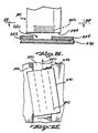
- FIGURES 9-11 A fringe field capacitance sensor capable of measuring both hole geometry and surface profile is illustrated in FIGURES 9-11.
- the sensor 100 comprises an elongated structure that includes probe 102 having electrodes 104-107 embedded therein. As described below, each electrode is connected to a suitable capacitance measuring circuit. Electrodes 104 and 106 are positioned along axis 110 and electrodes 105 and 107 are positioned along axis 112, axes 110 and 112 being perpendicular to one another and both being perpendicular to longitudinal axis 114 of sensor 100. The plane of each electrode is also perpendicular to axis 114.
- Probe 102 is adapted for positioning in hole 116, the diameter of probe 102 being selected such that it is somewhat less (e.g., 0.5 millimeters less) than the diameter of the hole. In FIGURES 10 and 11, the diameter of hole 116 relative to probe 102 has been somewhat exaggerated for ease of illustration. Probe 102 is positioned in hole 116 such that the probe adjacent one electrode, such as electrode 106 in FIGURE 11, rests directly on (i.e., is tangent to) the hole wall to make surface profile measurements, while the other electrodes are spaced from the hole wall to make distance measurements.
- the diameter of the hole along axis 110 can be determined by adding the spacing detected by electrode 104 to the probe diameter, while the diameter along axis 112 can be obtained by adding the distances measured by electrodes 105 and 107 to the probe diameter.
- Both the surface profile and geometry of hole 116 can therefore both be determined by sensor 100 by passing the probe axially through the hole, with the probe adjacent electrode 106 in contact with the hole wall. More detailed measurements can readily be obtained by providing additional electrodes, by rotating the sensor about axis 114 as the probe is moved along such axis, and/or by making multiple passes of the probe into and out of the hole.
- Sensor 100 comprises probe 102, stem 118, plate 120 and sleeve 122.
- Probe 102 comprises disks 124 and 126, disk 126 including mounting stem 128.
- the disks are preferably fabricated from a ceramic material, such as MACOR.
- Electrodes 104-107 are deposited on face 130 of disk 126, preferably by evaporative metal deposition. In one suitable technique, chromium is first deposited to establish a good bond with the MACOR, then a layer of silver is deposited to produce a total electrode thickness of approximately 0.1 micrometers. Four electrodes are deposited, each 1.6 millimeters wide and oriented at an angle of 90° with respect to one another.
- the entire probe 102 can then be turned down to the desired shape on a lathe.
- the diameter of probe 102 is preferably approximately 1.0 millimeters or less below the nominal diameter of the hole to be measured.
- the relief space created by the probe diameter being less than the hole diameter provides for ease of insertion and prevents the probe from jamming inside the hole due to misalignment.
- the appropriate relief space is a significant parameter, because the sensitivity quickly decreases as the electrodes get farther away from the hole wall. For a given application, optimal spacing can be determined from static calibration curves.
- Stem 118 comprises a stainless steel tube, the purpose of the stem being to support the probe and to serve as a shield for wires 132.
- Plate 120 is mounted within stem 118, and wires 132 are embedded in thin grooves along each side of the plate.
- a suitable material for plate 120 is Plexiglass sheet material.
- the wires are preferably spaced with respect to one another and with respect to stem 118 to minimize the total capacitance created by the stem and wires.
- Sleeve 122 provides a mounting for stem 118 and may have any suitable construction.
- FIGURE 12 illustrates a system for measuring the geometry and surface profile of a hole by means of sensor 100.
- the system comprises four detector circuits 140-143, multiplexer 144 and reference circuit 146.
- Detector circuit 140 includes commparator 148, NOR -gate 149, resistor 150, diode 151 and variable capacitance C1, capacitor C1 corresponding to the fringe field capacitance between electrode 104 and the body in which hole 116 has been drilled.
- Detector circuits 141-143 are identical to detector circuit 140, except that detector circuits 141-143 comprise variable capacitors C2-C4 (not shown) that correspond to the fringe field capacitance between electrodes 105-107 and the body in which hole 116 has been drilled. The body is assumed to be at ground potential.
- Reference circuit 146 comprises comparator 152, NOR gate 153, diode 154, resistor 155 and variable reference capacitor C R .
- the reference circuit is connected to the multiplexer 144 through line pair 160, and detector circuits 140-143 are connected to multiplexer 144 by line pairs 161-164, respectively.
- multiplexer In response to an address on address lines 156, multiplexer connects line pair 160 to one of line pairs 161-164.
- the detector and reference circuits comprise a differential pulse width modulation sensor that produces a square wave output signal on line pair 158 that has a duty cycle related to the relative magnitudes of capacitors C1 and C R .
- the frequency of the square wave signal on line pair 158 is typically on the order of 200-300 kilohertz.
- Lowpass filter 170 averages the signal on line pair 158 to produce a slowly varying differential signal on lines 172 that is converted by differential amplifier 174 into a single ended analog signal on line 176.
- the signal is again filtered by lowpass filter 177 to produce an analog signal 178 that is converted to a digital capacitance signal by A/D converter 179.
- the resulting capacitance signal on line 182 is input to measurement and control system 180.
- Measurement and control system 180 may comprise a Fluke 2450 measurement and control system or its equivalent.
- the measurement and control system controls the movement of sensor 100 into and out of hole 116 via position sense/control circuit 186, movement commands being transmitted to the position sense/control circuit via line 188, and signals indicative of sensor movement being transmitted to measurement and control system 180 via line 190.
- the measurement and control system also controls multiplexer 144 via address lines 156 to cause the multiplexer to selectively activate the detector circuits. During the time that a particular detector circuit is activated, the measurement and control system determines and stores the distal capacitance signal on line 182, and the corresponding probe position.
- the capacitance and position data may be processed directly by the measurement and control system, and/or transferred to a process control computer via a serial data link.
- each detector circuit 140-143 for example detector circuit 140, is an essentially linear function of the capacitance C1 as long as C R is selected to be of approximately the same magnitude as C1.
- the amplitude V of the capacitance signal on line 182 may therefore be written:
- the constants A and B may be obtained by routine calibration techniques.
- the probe 102 and electrode 106 can be positioned above the polished surface of a straight hole, and the signal on line 182 can then be recorded every 0.4 microns as a function of vertical displacement.
- the coefficients A and B can then be determined by a suitable least squares curve fit technique.
- Equation (1) is a good approximation of the capacitance C for comparatively small values of h.
- the capacitance is given by:
- the signal amplitude V is then
- the three variables A ⁇ , B ⁇ and H in equation (12) are adjusted iteratively until the least squares error is a minimum.
- the electrode height H is treated as an unknown because of the complex geometry of the ground surfaces around the electrode.
- FIGURE 13 sets forth a suitable sequence of operations for measurement and control system 180.
- the system commences inspection of a new hole at block 200 by moving the probe to a starting position at the hole entrance. The starting position is adjusted such that one of the four electrodes, e.g., electrode 106, is positioned tangent to the hole surface.
- detector circuit 140 corresponding to tangential electrode 106 is first activated by means of an appropriate command on address lines 156, and the probe is then moved into the hole.
- raw surface profile data is acquired at equal distance increments, for example every 5 micrometers, along the axis of the hole.
- probe motion is reversed at block 206, and the probe begins to move back out of the hole.
- detector circuits 140-143 are activated sequentially by multiplexer 144 in response to addresses supplied by the measurement and control system. Each time a detector circuit is activated, the measurement and control system acquires and stores the raw distance data, such data acquisition occurring, for example, every 50 micrometers along the hole axis. At the end of the reverse motion phase, the probe is retracted from the hole at block 208.
- the sequential activation of the detector circuits such that only one such circuit is activated at any one time, prevents crosstalk and interference between the measurements made through the several electrodes, and is a preferred aspect of the present invention.
- the measurement and control system converts the raw geometry data acquired during the reverse motion phase into diameters along axes 110 and 112 by means of equation (12), such diameters being tabulated as a function of distance along the hole axis.
- the refined geometry data is compared with preestablished criteria, and a decision is made whether to accept or reject the hole. The actions (if any) taken at this point upon hole rejection depend upon the particular process in which the probe is employed. In any case if the hole is accepted, the measurement and control system proceeds at block 214 to convert the raw profile data acquired during forward motion phase into a surface profile by converting the frequency measurements into heights by means of equation (10).
- the surface profile data may then be refined in block 216 by means of a dynamic compensation technique exemplified by equation (7).
- the refined surface profile data is examined to identify isolated surface defects.
- Profile parameters such as skewness, kurtosis and surface spectra may also be determined at block 218.
- the results of the analysis in block 218 are compared with preestablished criteria in block 220, and a decision is made to accept or reject the hole.
- the geometry and profile results are reported to a process control computer, and inspection of the hole is complete.
- the sensor of the present invention is suitable in many circumstances for measuring surface topography, i.e., the macroscopic shape and contour of a surface.
- many composite structures are formed from layers of graphite fiber "tape" impregnated with epoxy resin.
- the tape is typically 100 micrometers thick and 150 millimeters or more wide.
- the width of the gap between adjacent tapes is an important parameter in determining the overall quality of the composite structure.
- the tapes are layed down by high-speed automated equipment. Since each layer of tape is eventually covered by another layer, the task of measuring the gap between adjacent tapes must be accomplished during the tape lay-down process. The continuous measurement of the gap width is useful both for process monitoring and for control of the lay-down operation.
- the width of the gap may vary from less than 0 (i.e., overlap) to 7 millimeters or more.
- the required accuracy of the gap measurement is on the order of 100 micrometers.
- Surface contamination, low contrast, and mechanical vibrations have heretofore limited the application of optical methods of imaging and measuring the gap width.
- FIGURE 14 illustrates gap 230 formed between graphite tapes 232 and 234 that have been layed down on underlying tape 236.
- the gap width is measured by a sensor comprising ceramic probe 240 in which a plurality of electrodes 242 are embedded.
- the electrodes are aligned parallel to one another in three rows, as indicated in FIGURE 15, each electrode being perpendicular to lower surface 244 of probe 240 and to the top surfaces of tapes 232, 234 and 236.
- the staggered arrangement allows wider electrodes for increased sensitivity, and diminishes cross-coupling between the electrodes.
- Each electrode extends to and is flush with lower surface 244.
- the probe is inclined with respect to the boundaries 246, 248 of gap 230 such that the electrodes are spaced from one another in a direction normal to such boundaries.
- the inclination of the probe and the spacing of the electrodes within the probe are such that the electrodes are evenly spaced from one another along a measurement direction perpendicular to boundaries 246 and 248, as indicated in FIGURE 14.
- Electrodes 242 are each connected in a suitable capacitance measuring circuit, such as the detector circuits shown in FIGURE 12. The detector circuits are sequentially activated, and the distance from each electrode to the underlying surface is determined as probe 240 moves along the gap in the scanning direction indicated by arrow 250.
- probe 240 may be positioned and moved directly behind the apparatus for laying down the tapes. An image is thereby produced of the height of the surface along the measurement direction as a function of position along the gap. As predicted by equation (4) above, this image becomes sharper as the probe is moved closer to the underlying surface.
- the image may be processed by appropriate techniques to determine the positions of boundaries 246 and 248, from which the width of gap 230 as a function of position along the gap may be determined.
- a suitable technique for locating the positions of boundaries 246 and 248 is to locate the point at which the height changes most rapidly with respect to distance along the measurement direction.
- FIGURES 14 and 15 illustrate one specific application of the present invention to the measurement of surface topography. It will be appreciated, however, that numerous variations will be appropriate for different applications. For example, a single electrode could be scanned along a surface (e.g. back and forth across a gap) to measure the width of a gap or other features of a surface. Stationary or moving arrays of electrodes can readily be constructed to optimise the measurement of any required surface shape.
Landscapes
- Physics & Mathematics (AREA)
- General Physics & Mathematics (AREA)
- Measurement Of Length, Angles, Or The Like Using Electric Or Magnetic Means (AREA)
- Measurement Of Levels Of Liquids Or Fluent Solid Materials (AREA)
- Arrangements For Transmission Of Measured Signals (AREA)
Claims (20)
8. Appareil selon la revendication 6, caractérisé en ce que l'épaisseur de l'armature (20; 104, 105, 106, 107; 242) est notablement inférieure à la longueur d'onde caractéristique (λ).
Priority Applications (1)
| Application Number | Priority Date | Filing Date | Title |
|---|---|---|---|
| AT86306192T ATE60436T1 (de) | 1985-08-09 | 1986-08-11 | Kapazitiver streufeldsensor und verfahren. |
Applications Claiming Priority (2)
| Application Number | Priority Date | Filing Date | Title |
|---|---|---|---|
| US06/764,164 US4814691A (en) | 1985-08-09 | 1985-08-09 | Fringe field capacitive sensor for measuring profile of a surface |
| US764164 | 2001-01-16 |
Publications (2)
| Publication Number | Publication Date |
|---|---|
| EP0221638A1 EP0221638A1 (fr) | 1987-05-13 |
| EP0221638B1 true EP0221638B1 (fr) | 1991-01-23 |
Family
ID=25069862
Family Applications (1)
| Application Number | Title | Priority Date | Filing Date |
|---|---|---|---|
| EP86306192A Expired - Lifetime EP0221638B1 (fr) | 1985-08-09 | 1986-08-11 | Palpeur capacitif en champ de dispersion et procédé |
Country Status (5)
| Country | Link |
|---|---|
| US (1) | US4814691A (fr) |
| EP (1) | EP0221638B1 (fr) |
| AT (1) | ATE60436T1 (fr) |
| CA (1) | CA1279988C (fr) |
| DE (1) | DE3677137D1 (fr) |
Families Citing this family (37)
| Publication number | Priority date | Publication date | Assignee | Title |
|---|---|---|---|---|
| JP2690908B2 (ja) * | 1987-09-25 | 1997-12-17 | 株式会社日立製作所 | 表面計測装置 |
| US4996492A (en) * | 1989-03-07 | 1991-02-26 | The Boeing Company | Probe for inspecting countersunk holes in conductive bodies |
| US5021740A (en) * | 1989-03-07 | 1991-06-04 | The Boeing Company | Method and apparatus for measuring the distance between a body and a capacitance probe |
| EP0425823A1 (fr) * | 1989-09-29 | 1991-05-08 | Antivision Systems Corp. | Système électrostatique pour former des images |
| US5281921A (en) * | 1990-04-24 | 1994-01-25 | Novak James L | Non-contact capacitance based image sensing method and system |
| US5189377A (en) * | 1990-09-04 | 1993-02-23 | Extrude Hone Corporation | Method and apparatus for co-ordinate measuring using a capacitance probe |
| GB9021448D0 (en) * | 1990-10-03 | 1990-11-14 | Renishaw Plc | Capacitance sensing probe |
| GB9021447D0 (en) * | 1990-10-03 | 1990-11-14 | Renishaw Plc | Capacitance probes |
| GB2265720B (en) * | 1990-11-16 | 1995-06-14 | Moonstone Designs Ltd | Device for determining the presence and/or characteristics of an object or a substance |
| US5272443A (en) * | 1992-04-22 | 1993-12-21 | Aluminum Company Of America | Chatter and profile measuring using capacitor sensors |
| US5365166A (en) * | 1993-02-08 | 1994-11-15 | Westinghouse Electric Corporation | System and method for testing electrical generators |
| DE4304451C2 (de) * | 1993-02-13 | 1995-12-14 | Seichter Gmbh | Meßsystem zur Erfassung von Unebenheiten auf der Oberfläche eines Meßobjektes |
| US5517190A (en) * | 1994-02-03 | 1996-05-14 | Gunn; Colin N. | Physical measurement from changes in reactance |
| US5646538A (en) * | 1995-06-13 | 1997-07-08 | Measurement Systems, Inc. | Method and apparatus for fastener hole inspection with a capacitive probe |
| EP0790479B1 (fr) | 1996-02-14 | 2002-01-16 | STMicroelectronics S.r.l. | Capteur capacitif de distance, en particulier pour la prise d'empreintes digitales |
| US6114862A (en) | 1996-02-14 | 2000-09-05 | Stmicroelectronics, Inc. | Capacitive distance sensor |
| US6320394B1 (en) | 1996-02-14 | 2001-11-20 | Stmicroelectronics S.R.L. | Capacitive distance sensor |
| US6483931B2 (en) | 1997-09-11 | 2002-11-19 | Stmicroelectronics, Inc. | Electrostatic discharge protection of a capacitve type fingerprint sensing array |
| US6028773A (en) * | 1997-11-14 | 2000-02-22 | Stmicroelectronics, Inc. | Packaging for silicon sensors |
| US6191593B1 (en) | 1997-12-17 | 2001-02-20 | Stmicroelectronics, Inc. | Method for the non-invasive sensing of physical matter on the detection surface of a capacitive sensor |
| US6091082A (en) * | 1998-02-17 | 2000-07-18 | Stmicroelectronics, Inc. | Electrostatic discharge protection for integrated circuit sensor passivation |
| US6181142B1 (en) * | 1998-07-21 | 2001-01-30 | Ade Corporation | Nonlinear current mirror for loop-gain control |
| US6397158B1 (en) * | 1999-04-29 | 2002-05-28 | Sun Microsystems, Inc. | Method for determining capacitance values for quieting noisy power conductors |
| US7239227B1 (en) | 1999-12-30 | 2007-07-03 | Upek, Inc. | Command interface using fingerprint sensor input system |
| US6512381B2 (en) | 1999-12-30 | 2003-01-28 | Stmicroelectronics, Inc. | Enhanced fingerprint detection |
| US6618505B2 (en) | 2000-03-09 | 2003-09-09 | The Boeing Company | Method, apparatus and computer program product for determining shim shape |
| US6943665B2 (en) * | 2000-03-21 | 2005-09-13 | T. Eric Chornenky | Human machine interface |
| US20030098774A1 (en) * | 2000-03-21 | 2003-05-29 | Chornenky Todd E. | Security apparatus |
| US7137300B2 (en) * | 2003-03-19 | 2006-11-21 | California Institute Of Technology | Parylene capacitive accelerometer utilizing electrical fringing field sensing and method of making |
| US8115497B2 (en) * | 2007-11-13 | 2012-02-14 | Authentec, Inc. | Pixel sensing circuit with common mode cancellation |
| RU2504730C1 (ru) * | 2012-07-19 | 2014-01-20 | Федеральное Государственное Унитарное Предприятие "Государственный научно-производственный ракетно-космический центр "ЦСКБ-Прогресс" (ФГУП "ГНПРКЦ "ЦСКБ-Прогресс") | Способ контроля целостности токопроводящего покрытия на диэлектрическом материале |
| JP6017096B1 (ja) * | 2015-10-30 | 2016-10-26 | 三菱電機株式会社 | ワイヤ放電加工機、ワイヤ放電加工機の制御装置の制御方法及び位置決め方法 |
| US9817439B2 (en) | 2016-02-29 | 2017-11-14 | JumpStartCSR, Inc. | System, method and device for designing, manufacturing, and monitoring custom human-interfacing devices |
| WO2017195001A1 (fr) * | 2016-05-13 | 2017-11-16 | Arcelormittal | Procédé d'obtention de la hauteur d'un matériau empilé dans un four à coke |
| EP3335872A1 (fr) | 2016-12-16 | 2018-06-20 | Amcor Flexibles Winterbourne Limited | Films polymères et emballages ainsi obtenus |
| WO2020012440A1 (fr) * | 2018-07-12 | 2020-01-16 | Scuola Superiore Di Studi Universitari E Di Perfezionamento Sant'anna | Système sensible de détection de proximité accrue |
| US11480428B2 (en) * | 2019-01-09 | 2022-10-25 | The Boeing Company | Methods and systems to test a size or characteristic of a hole |
Family Cites Families (20)
| Publication number | Priority date | Publication date | Assignee | Title |
|---|---|---|---|---|
| US2802178A (en) * | 1954-09-22 | 1957-08-06 | Gen Electric | Motion detecting device |
| US3400331A (en) * | 1965-01-18 | 1968-09-03 | Pratt & Whitney Inc | Gaging device including a probe having a plurality of concentric and coextensive electrodes |
| US3504279A (en) * | 1967-09-27 | 1970-03-31 | Reliance Electric & Eng Co | Noncontact interrupted surface inspection apparatus providing an electrical analog of the surface profile |
| US3805150A (en) * | 1970-08-17 | 1974-04-16 | Ade Corp | Environment immune high precision capacitive gauging system |
| US3842194A (en) * | 1971-03-22 | 1974-10-15 | Rca Corp | Information records and recording/playback systems therefor |
| GB1436698A (en) * | 1972-02-11 | 1976-05-19 | Bakelite Xylonite Ltd | Apparatus for thickness measurement |
| US3771051A (en) * | 1972-06-14 | 1973-11-06 | Ade Corp | Apparatus and method for indicating surface roughness |
| FR2202586A5 (fr) * | 1972-10-06 | 1974-05-03 | Commissariat Energie Atomique | |
| GB1483187A (en) * | 1973-10-22 | 1977-08-17 | Ici Ltd | Method of and apparatus for assessing the flatness of anodes |
| US4103226A (en) * | 1976-09-15 | 1978-07-25 | Westinghouse Electric Corp. | Apparatus for gauging the texture of a conducting surface |
| US4112355A (en) * | 1976-10-22 | 1978-09-05 | Lockheed Corporation | Quality and fit measuring apparatus for fasteners and their holes |
| US4168465A (en) * | 1977-12-15 | 1979-09-18 | The United States Of America As Represented By The Secretary Of The Air Force | Tapered hole capacitive probe |
| GB2015165B (en) * | 1978-02-09 | 1983-01-12 | Koa Oil Co Ltd | Detecting capacitively corrosion of pipes |
| US4152641A (en) * | 1978-02-27 | 1979-05-01 | Rca Corporation | Method and apparatus for the determination of signal pickup qualities of a stylus of a capacitive disc video player |
| DD136897B1 (de) * | 1978-06-20 | 1981-03-25 | Elektromat Veb | Kapazitiver messfuehler |
| US4296371A (en) * | 1980-03-17 | 1981-10-20 | Rca Corporation | System for measuring stylus shoe length |
| US4352060A (en) * | 1980-07-01 | 1982-09-28 | Viak Ab | Apparatus for measuring the interior dimensions of a cast iron mold |
| GB2100441A (en) * | 1981-06-12 | 1982-12-22 | Automatic Systems Lab Ltd | Method for determining dimensions and/or form of surfaces |
| US4481616A (en) * | 1981-09-30 | 1984-11-06 | Rca Corporation | Scanning capacitance microscope |
| US4422035A (en) * | 1981-12-11 | 1983-12-20 | Extrude Hone Corporation | Capacitance measurement probe |
-
1985
- 1985-08-09 US US06/764,164 patent/US4814691A/en not_active Expired - Lifetime
-
1986
- 1986-08-11 CA CA000515648A patent/CA1279988C/fr not_active Expired - Lifetime
- 1986-08-11 AT AT86306192T patent/ATE60436T1/de not_active IP Right Cessation
- 1986-08-11 DE DE8686306192T patent/DE3677137D1/de not_active Expired - Lifetime
- 1986-08-11 EP EP86306192A patent/EP0221638B1/fr not_active Expired - Lifetime
Also Published As
| Publication number | Publication date |
|---|---|
| DE3677137D1 (de) | 1991-02-28 |
| CA1279988C (fr) | 1991-02-12 |
| US4814691A (en) | 1989-03-21 |
| EP0221638A1 (fr) | 1987-05-13 |
| ATE60436T1 (de) | 1991-02-15 |
Similar Documents
| Publication | Publication Date | Title |
|---|---|---|
| EP0221638B1 (fr) | Palpeur capacitif en champ de dispersion et procédé | |
| US4935700A (en) | Fringe field capacitive sensor for measuring the size of an opening | |
| US6801044B2 (en) | Universal electromagnetic resonance system for detecting and measuring local non-uniformities in metal and non-metal objects | |
| Wyant et al. | Development of a three-dimensional noncontact digital optical profiler | |
| US6408677B1 (en) | Calibration disk having discrete bands of composite roughness | |
| US6593738B2 (en) | Method and apparatus for measuring thickness of conductive films with the use of inductive and capacitive sensors | |
| US6657429B1 (en) | Material condition assessment with spatially periodic field sensors | |
| US7161350B2 (en) | Method for material property monitoring with perforated, surface mounted sensors | |
| US7589526B2 (en) | Surface mounted sensor arrays having segmented primary windings | |
| US5525903A (en) | Eddy current method of acquiring the surface layer properties of a metallic target | |
| US7994781B2 (en) | Eddy current sensor with concentric segments | |
| Sherrington et al. | Modern measurement techniques in surface metrology: part I; stylus instruments, electron microscopy and non-optical comparators | |
| CA2090978A1 (fr) | Methode et dispositif de mesure utilisant un capteur capacitif se deplacant dans les trois axes | |
| US20050248339A1 (en) | Segmented field sensors | |
| US5558692A (en) | Optical waveguide preform measurement during manufacture | |
| Garbini et al. | In-process drilled hole inspection for aerospace applications | |
| EP0067643A2 (fr) | Méthode pour déterminer les dimensions et/ou la forme de surfaces | |
| GB2100441A (en) | Method for determining dimensions and/or form of surfaces | |
| Garbini et al. | Surface profile measurement during turning using fringe-field capacitive profilometry | |
| Murugarajan et al. | Measurement, modeling and evaluation of surface parameter using capacitive-sensor-based measurement system | |
| Garbini et al. | Surface profilometry based on fringing capacitance measurement | |
| Griffiths et al. | Light scattering for the measurement of surface finish: a review | |
| Briggs et al. | Unshielded capacitor probe technique for determining disk memory ceramic slider flying characteristics | |
| Bhushan | Solid surface characterization | |
| Woolley | Pneumatic method for making fast, higher resolution, noncontacting measurement of surface topography |
Legal Events
| Date | Code | Title | Description |
|---|---|---|---|
| PUAI | Public reference made under article 153(3) epc to a published international application that has entered the european phase |
Free format text: ORIGINAL CODE: 0009012 |
|
| AK | Designated contracting states |
Kind code of ref document: A1 Designated state(s): AT BE CH DE FR GB IT LI LU NL SE |
|
| 17P | Request for examination filed |
Effective date: 19871106 |
|
| 17Q | First examination report despatched |
Effective date: 19890317 |
|
| GRAA | (expected) grant |
Free format text: ORIGINAL CODE: 0009210 |
|
| ITF | It: translation for a ep patent filed | ||
| RAP1 | Party data changed (applicant data changed or rights of an application transferred) |
Owner name: WASHINGTON RESEARCH FOUNDATION |
|
| AK | Designated contracting states |
Kind code of ref document: B1 Designated state(s): AT BE CH DE FR GB IT LI LU NL SE |
|
| PG25 | Lapsed in a contracting state [announced via postgrant information from national office to epo] |
Ref country code: BE Effective date: 19910123 Ref country code: AT Effective date: 19910123 |
|
| REF | Corresponds to: |
Ref document number: 60436 Country of ref document: AT Date of ref document: 19910215 Kind code of ref document: T |
|
| REF | Corresponds to: |
Ref document number: 3677137 Country of ref document: DE Date of ref document: 19910228 |
|
| ET | Fr: translation filed | ||
| PG25 | Lapsed in a contracting state [announced via postgrant information from national office to epo] |
Ref country code: LU Free format text: LAPSE BECAUSE OF NON-PAYMENT OF DUE FEES Effective date: 19910831 |
|
| PLBE | No opposition filed within time limit |
Free format text: ORIGINAL CODE: 0009261 |
|
| STAA | Information on the status of an ep patent application or granted ep patent |
Free format text: STATUS: NO OPPOSITION FILED WITHIN TIME LIMIT |
|
| 26N | No opposition filed | ||
| EAL | Se: european patent in force in sweden |
Ref document number: 86306192.5 |
|
| PGFP | Annual fee paid to national office [announced via postgrant information from national office to epo] |
Ref country code: SE Payment date: 19960819 Year of fee payment: 11 |
|
| PGFP | Annual fee paid to national office [announced via postgrant information from national office to epo] |
Ref country code: NL Payment date: 19960831 Year of fee payment: 11 |
|
| PG25 | Lapsed in a contracting state [announced via postgrant information from national office to epo] |
Ref country code: SE Free format text: LAPSE BECAUSE OF NON-PAYMENT OF DUE FEES Effective date: 19970812 |
|
| PG25 | Lapsed in a contracting state [announced via postgrant information from national office to epo] |
Ref country code: NL Free format text: LAPSE BECAUSE OF NON-PAYMENT OF DUE FEES Effective date: 19980301 |
|
| EUG | Se: european patent has lapsed |
Ref document number: 86306192.5 |
|
| NLV4 | Nl: lapsed or anulled due to non-payment of the annual fee |
Effective date: 19980301 |
|
| REG | Reference to a national code |
Ref country code: GB Ref legal event code: IF02 |
|
| PGFP | Annual fee paid to national office [announced via postgrant information from national office to epo] |
Ref country code: GB Payment date: 20040812 Year of fee payment: 19 |
|
| PGFP | Annual fee paid to national office [announced via postgrant information from national office to epo] |
Ref country code: CH Payment date: 20040817 Year of fee payment: 19 |
|
| PGFP | Annual fee paid to national office [announced via postgrant information from national office to epo] |
Ref country code: FR Payment date: 20040831 Year of fee payment: 19 |
|
| PGFP | Annual fee paid to national office [announced via postgrant information from national office to epo] |
Ref country code: DE Payment date: 20040917 Year of fee payment: 19 |
|
| PG25 | Lapsed in a contracting state [announced via postgrant information from national office to epo] |
Ref country code: IT Free format text: LAPSE BECAUSE OF NON-PAYMENT OF DUE FEES;WARNING: LAPSES OF ITALIAN PATENTS WITH EFFECTIVE DATE BEFORE 2007 MAY HAVE OCCURRED AT ANY TIME BEFORE 2007. THE CORRECT EFFECTIVE DATE MAY BE DIFFERENT FROM THE ONE RECORDED. Effective date: 20050811 Ref country code: GB Free format text: LAPSE BECAUSE OF NON-PAYMENT OF DUE FEES Effective date: 20050811 |
|
| PG25 | Lapsed in a contracting state [announced via postgrant information from national office to epo] |
Ref country code: LI Free format text: LAPSE BECAUSE OF NON-PAYMENT OF DUE FEES Effective date: 20050831 Ref country code: CH Free format text: LAPSE BECAUSE OF NON-PAYMENT OF DUE FEES Effective date: 20050831 |
|
| PG25 | Lapsed in a contracting state [announced via postgrant information from national office to epo] |
Ref country code: DE Free format text: LAPSE BECAUSE OF NON-PAYMENT OF DUE FEES Effective date: 20060301 |
|
| REG | Reference to a national code |
Ref country code: CH Ref legal event code: PL |
|
| GBPC | Gb: european patent ceased through non-payment of renewal fee |
Effective date: 20050811 |
|
| PG25 | Lapsed in a contracting state [announced via postgrant information from national office to epo] |
Ref country code: FR Free format text: LAPSE BECAUSE OF NON-PAYMENT OF DUE FEES Effective date: 20060428 |
|
| REG | Reference to a national code |
Ref country code: FR Ref legal event code: ST Effective date: 20060428 |