EP0222021A1 - Convertisseur numerique/analogique - Google Patents
Convertisseur numerique/analogique Download PDFInfo
- Publication number
- EP0222021A1 EP0222021A1 EP86902912A EP86902912A EP0222021A1 EP 0222021 A1 EP0222021 A1 EP 0222021A1 EP 86902912 A EP86902912 A EP 86902912A EP 86902912 A EP86902912 A EP 86902912A EP 0222021 A1 EP0222021 A1 EP 0222021A1
- Authority
- EP
- European Patent Office
- Prior art keywords
- circuit
- signal
- digital input
- digital
- supplied
- Prior art date
- Legal status (The legal status is an assumption and is not a legal conclusion. Google has not performed a legal analysis and makes no representation as to the accuracy of the status listed.)
- Granted
Links
Images


Classifications
-
- H—ELECTRICITY
- H03—ELECTRONIC CIRCUITRY
- H03M—CODING; DECODING; CODE CONVERSION IN GENERAL
- H03M1/00—Analogue/digital conversion; Digital/analogue conversion
- H03M1/66—Digital/analogue converters
-
- G—PHYSICS
- G06—COMPUTING OR CALCULATING; COUNTING
- G06J—HYBRID COMPUTING ARRANGEMENTS
- G06J1/00—Hybrid computing arrangements
Definitions
- This invention relates generally to a D/A converter which converts a digital signal into an analog signal (hereinafter be simply referred to as "the D/A conversion"), and more particularly to an integrating type D/A conveter which is preferably adapted to convert a plurality of dogital signals into an analog output signal.
- reference numeral 1 designates an input terminal to which a digital signal is supplied and this input terminal 1 has n terminals 1 0 , 1 1 , 1 2 , ..., 1 n corresponding to the number of bits of a digital signal to be inputted thereto.
- the digital signal having n bits is parallelly inputted such that the most significant bit (MSB) thereof is supplied to the terminal 1 0 , the bit next to the MSB to the termnal 1 1 , respective bits are supplied sequentially to the respective terminals in the same manner, and finally the least significant bit (LSB) thereof is supplied to the terminal 1 n .
- MSB most significant bit
- LSB least significant bit
- the n-bit digital signals simultaneously inputted to the terminals 1 0 - 1 n are supplied to a data register 2 through input terminal groups 3 and 4 in predetermined conditions.
- the input terminal groups 3 and 4 respectively have m and (m-n-1) input terminals 3 0 - 3 m and 4 0 - 4 m .
- the terminal 1 0 is connected only to the terminal 3 0 , and the terminal 1 n only to the terminal 4 m .
- the terminal 1 1 is connected to input terminals 3 1 and 4 0 , the terminal 1 2 to terminals 3 1 and 4 1 , and in the same manner, respective terminals of the input terminal group 1 are connected to respective input terminals of the input terminal groups 3 and 4.
- the input terminal 3 0 of the data register 2 is supplied with the most significant bit of the input digital signal, the input terminal 3 1 with the bit next to the most significant bit of the same input digital signal, and in the same manner as above, the respective input terminals 3 2 , 3 3 , ..., 3 m are supplied with the respective bits of the digital input signal.
- the input terminal 4 0 of the data register 2 is supplied with the second most significant bit of the input digital signal, the input terminal 4 1 with the third significant bit of the same, and in the same manner, respective input terminals 4 2 , 4 3 , ..., 4 m are sequentially supplied with the respective bits of the digital input signal.
- the input terminal 4m is supplied with the least significant bit of the input digital signal supplied to the terminal lm.
- the data register 2 switches the digital signals inputted to the input terminal groups 3 and 4 and delivers the same to an output terminal group 5 which has m output terminals 5 0 , 5 1 , ..., 5 m .
- the digital signal outputted to the output terminal group 5, i.e. the signal inputted to the input terminal group 3 or that inputted to the input terminal group 4, is selected by a change-over control signal supplied from a control circuit 7 to the data register 2 through its control terminal 6.
- delivered to the output terminal group 5 is, in response to the switching operation by the data register 2, either the digital signal from the input terminal group 3, that is, the digital signal comprising from the most significant bit to the second least significant bit or the digital signal from the input terminal group 4, that is, the digital signal comprising from the second most significant bit to the least significant bit.
- the manner which of the digital signals supplied to the input terminal groups 3 and 4 is delivered to the output terminal 5 of the data register 2 by switching the same is based upon the result of a determination made as to whether or not the information area of the inputted digital signal exceeds a predetermined information area.
- Information indicative of the information area of the inputted digital signal can be obtained on the basis of a predetermined number of digits of bit information including the MSB of the inputted digital signal.
- the above-mentioned determination operation is effected by the control circuit 7.
- This control circuit 7 determines whether or not the information area of the inputted digital signal exceeds the predetermined information area on the basis of the predetermined number of digits of bit information including the most significant bit of the inputted digital signal and generates an information area signal (a change-over control signal) according to the determination result.
- the signal generated by the control circuit 7 is supplied to the control terminal 6 of the data register 2 and a control terminal 9 of another data register 8, as will be later described.
- the data registers 2 and 8 carry out the changing operation in response to the information area state in the digital input signals. To be specific, if the digital input signal occupies an information area which is more than one half of the full scale, the data register 2 delivers the digital signal in the input terminal group 3 to the output terminal group 5. On the other hand, if the digital input signal is the signal of the information area less than one half of the full scale, the data register 2 delivers the digital signal in the input terminal group 4 to the output terminal group 5.
- the output from the data register 2 is supplied to a latch circuit 10 and this latch circuit 10 latches the digital signal from the data register 2 and supplies the same to a D/A converter 12 at the time a latch signal is applied thereto from a terminal 11.
- the D/A converter 12 is a multiplication type one which is provided with an external reference input terminal 13. To this input terminal 13 is supplied an external reference signal generated from another D/A converter 14.
- the data register 8 has two input terminal groups 15 and 16 such that two digital signals, generated from a fixed data generating circuit 17, respectively indicative of different data are suppied thereto.
- the digital signal outputted from the data register 8 is latched by a latch circuit 19 and then supplied to the D/A converter 14 as an input signal, at the time the latch signal is supplied from the termainal 11 to the latch circuit.
- the D /A converter 14 converts the inputted digital signal into an analog signal and supplies the converted analog signal to the input terminal 13 of the D/A converter 12 as an external reference input signal (external reference voltage).
- the data register 2 delivers the digital signal in the input terminal group 3 to the output terminal group 5, the data register 8 outputs, to the output terminal group 18, the digital signal indicative of the one data supplied from the fixed data generating circuit 17 to the input terminal group 15.
- the data register 2 delivers the digital signal in the input terminal group 4 to the output terminal group 5, the data register 8' outputs, to the output terminal group 18, the digital signal indicative of the other data supplied from the fixed data generating circuit 17 to the input terminal group 16.
- the one data from the fixed data generating circuit 17 is one from which the D/A converter 14 can generate an external reference voltage V which is necessary to deliver to an output terminal 20 an analog signal extended in a predetermined manner from the input digital signal having an information area wider than one half of the full scale.
- the other data from the fixed data generating circuit 17 is one from which the D/A converter 14 can generate an external reference voltage V/2 which is necessary to deliver to the output terminal 20 an analog signal corresponding to the digital input signal having an information area narrower than one half of the full scale.
- the D/A converter is provided with an integration circuit 26, a current-voltage converting means 22 which converts a constant current from a constant current supplying circuit 21 into a current ratio, a switched capacitor 23 arranged between the current-voltage converting means and the above integration circuit and adapted to control the amount of electrical charge supplied to the integration circuit, control means 28, 31, 39 - 46 supplied with first and second digital input signals and for controlling turning on and off of the switched capacitor, and clock generating means 34, 35 for supplying a clock signal to the control means, the construction of which is such that an analog output signal corresponding to a product of the first and second digital input signals is derived from the output side of the integration circuit.
- the current-voltage converting means 22 converts the constant current from the constant current supplying circuit 21 to a voltage and supplies the same to the integration circuit 26 through the switched capacitor 23, and at the same time turning on and off of the switched capacitor is controlled by the control means 28, 31, 39 - 46 which are supplied with the first and second digital input signals, and thereby the analog output signal corresponding to a product of the first and second digital input signals is delivered to the output side of the integration circuit.
- Fig. 1 is a block diagram used to explain a prior art example
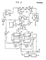
- Fig. 2 is a block diagram showing an embodiment according to the invention
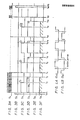
- Figs. 3 and 4 are signal wave form charts used to explain the operation of the embodiment shown in Fig. 2
- Figs. 5 - 7 are respectively block diagrams showing other embodiments according to the invention.
- Fig. 2 shows a circuit configuration of a first embodiment of the present invention.
- reference numeral 21 designates a constant current supplying circuit as a reference current source.
- the constant current from the constant current supplying circuit 21 is supplied to a current-voltage converting circuit 22 to be converted into a constant voltage which in turn is supplied to a switched capacitor 23.
- the switched capacitor 23 comprises a capacitor 23a and switches 23b and 23c respectively arranged at both ends of the capacitor 23a.
- a contact a of the switch 23b is connected to an output side of the current-voltage converter 22 while the other contact b thereof is grounded.
- a contact a of the switch 23c is connected to an inverting input terminal of an integration circuit 26 comprising a capacitor 24 and a differential amplifier 25 while the other contact b thereof is grounded.
- the switched capacitor 23 When the swithes 23b and 23c are changed over as indicated by solid lines in Fig. 2 by a control signal, hereinafter referred to, the switched capacitor 23 operates as a non inverting circuit.
- the switches 23b and 23c are changed over as indicated by broken lines in the same figure, it operates as an inverting circuit. That is, when the switched capacitor 23 operates as a non inverting circuit, if the switch 23b is connected to its contact a, the switch 23c is also connected to its contact a, and if the switch 23b is connected to its contact b, the switch 23c is also connected to its contact b.
- the constant voltage outputted from the current-voltage converter 22 is supplied through thus operating switched capacitor 23 to the integration circuit 26. From the output side of the integration circuit 26 led out is an output terminal 27.
- Reference numeral 34 designates a clock generator.
- a clock signal S 1 (Fig. 3A) from the clock generator 34 is supplied to a 1/16 frequency divider 25 as well as to a clock terminal of the counter 32 of the control signal generating circuit 31.
- An output signal S 3 (Fig. 3C) from the 1/16 frequency divider 35 is supplied to a clock terminal of the counter 29 as well as to a clear terminal of the counter 32 through an inverter 36 and an OR circuit 37.
- the counter 32 is reset at an edge, e.g. at a rising edge of the output signal.
- Reference numeral 38 is an input terminal to which is supplied a start signal S 2 (Fig. 3B) to turn the whole converter on.
- the start signal from the input terminal 38 is supplied to the 1/16 frequency divider 35 as a reset signal, a'clear terminal of the counter 29, and the clear terminal of the counter 32 through the OR circuit 37.
- control signals S 5 and S 4 generated from the control signal generating circuits 28 and 31 are both supplied to an AND circuit 39 and an output signal S 6 (Fig. 2F) of the AND circuit 39 is supplied to one input terminal of respective AND circuits 40 and 41.
- Reference numeral 42 designates a clock generator which generates clock singals to change over the switches 23b and 23c of the switched capacitor 23. Generated from the clock generator 42 are two clock signals S 7 and S 8 having opposite fase to one another as shown in Fig. 4. The signals S 7 and S 8 are respectively supplied to the other input terminals of the AND circuits 40 and 41.
- the AND circuits 40 and 41 operate so as to substantially mask the clock signals S 7 and S 8 from the clock generating circuit 42 by the use of the output signal S 6 from the AND circuit 39, whereby the switched capacitor 2 3 operates only when the control signals S 5 and S 4 are both outputted simultaneously.
- the output signal from the AND circuit 41 is directly used as a control signal for the switch 23c of the switched capacitor 23.
- the output signals from the AND circuits 40 and 41 are respectively supplied to one input terminal of AND circuits 43 and 44. Further, a bit (MSB) indicative of the polarity of the first digital input signal supplied to the comparator 30 and a bit (MSB) indicative of the polarity of the second digital input signal supplied to the comparator 33 are supplied to an exclusive OR circuit 45, the output signal of which is supplied to the other input terminal of the respective AND circuits 43 and 44.
- the output signal of the exclusive OR circuit 45 becomes low level when the first and second digital input signals have the same polarity, and high level when these signals have respectively the different polarities from each other.
- the AND circuits 43 and 44 substantially determine, by the bits indicative of the porality of the first and second input digital signals, which of the clock signals S 7 and S 8 derived from the clock generating circuit 42 is supplied to the switch 23b of the switched capacitor 23, to thereby change over the operation of the switched capacitor 23 from non inverting to inverting.
- the switch 23c of the switched capacitor 23 when the switch 23c of the switched capacitor 23 is supplied with the clock signal S 8 from the clock generator 42 through the AND circuit 41 if the switch 23b is supplied with the clock signal S8 from the clock generator circuit 42 through the AND circuit 44 and the OR circuit 46, the switched capacitor 23 operates as a non-inverting circuit, since there is the in-phase relationship between the signals supplied thereto.
- the switch 23b if the switch 23b is supplied with the signal S 7 from the clock generating circuit 42 through the AND circuit 43 and the OR circuit 46, the switched capacitor 23 operates as an inverting circuit, since there is the anti-phase relationship between the signals supplied thereto.
- the start signal S 2 as shown in Fig. 3B is supplied at a time to from the input terminal 33 to the 1/16 frequency divider 35, the clear terminal of the counter 29, and the counter 32 through the OR circuit 37. Then, at a time t 1 when the signal S 2 is fallen down, the 1/16 frequency divider 35 and counters 29 and 32 are reset. As a result, at the same time the output signal S 3 from the 1/16 frequency divider 35 becomes high level as shown in Fig. 3 C , the output signals (control signals) S 4 and S 5 from the control signal generating circuits 31 and 28 become high level, as shown respectively in Figs. 3D and 3E.
- the output signal S 6 from the AND circuit 39 also becomes high level, as shown in Fig. 3F.
- the clock signals S 7 and S s from the clock generator 42 pass therethrough.
- the clock signal S 8 through the AND circuit 41 is supplied to the switch 23c of the switched capacitor 23 as a control signal as it is and also to the AND circuit 44.
- the clock signal S 7 through the AND circuit 40 is supplied to the AND circuit 43.
- the AND circuit 44 closes its gate while the AND circuit 43 opens its gate, and consequently the clock signal S 7 through the AND circuit 43 is supplied through the OR circuit 46 to the switch 23b of the switched capacitor 23 as a control signal, whereby at that time the switched capacitor 23 operates as an inverting circuit.
- the constant voltage derived from the current-voltage converter 22 is accumulated in the capacitor 23a of the switched capacitor 23 operating as mentioned above, the constant voltage is supplied to the integration circuit 26 tc thereby start charging the capacitor 24.
- the counters 29 and 31 begin their operation at the time t l , the counter 29 is in a state to count the pulses of the signal S 3 supplied thereto from the 1/16 frequency divider 35, while the counter 31 starts sequentially counting the pulses of the clock signal S 1 , as shown in Fig. 3A, generated from the clock generator 34. Then, at the time t 2 the output signal from the 1/16 frequency divider 35 is inverted from high level to low level.
- the clock signals S 7 and S 8 from the clock generator 42 are not supplied to the switched capacitor 23, and therefore the integration circuit 26 is substantially inhibited from being supplied with the constant voltage derived from the constant current supplying circuit 21 through the current-voltage converting circuit 22 and the switched capacitor 23.
- the counter 29 starts counting pulses of the signal S 3 outputted from the 1/16 frequency divider 35, and the counter 32 is reset by the signal S 3 from the 1/16 frequency divier 35 and again starts counting pulses of the clock signal derived from the clock signal generator 34. Also at the time t 4 , the signal S 3 from the 1/16 frequency divider 35 is inverted from low level to high level.
- the signal S 3 from the 1/16 frequency divider 35 is again inverted from high level to low level.
- the same operations as those effected at the time t 3 are effected.
- the above-mentioned operations are repeated.
- the start signal S 2 is again supplied from the input terminal 38 to the 1/16 frequency divider 35 as a reset signal as well as to the clear terminals of the respective counters 29 and 32. Then, the above-mentioned operations during the time period between the times tl and t 3 are repeated in the same manner.
- the digital input signals supplied to the comparators 30 and 33 may have values different from those as determined above.
- an analog output converted from a product of two digital input signal values can be generated by setting N 1 and N 2 to values corresponding to the two digital input signal values.
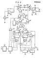
- Fig. 5 shows a circuit configuration of a second embodiment of the invention.
- the same reference numerals designate the same parts in Fig. 2 and the detailled description thereof is omitted.
- a digital signal supplied to an input terminal 47 is supplied to a difference processing circuit 48 wherein the difference between adjacent sampled values is obtained. Then, the output signal from the difference processing circuit 48 is supplied to a floating-point processing circuit 49 wherein the supplied signal is divided into signals indicative of a mantissa portion and an exponent portion. The mantissa portion is supplied to the comparator 30 as the first digital input signal, and the exponent portion to the comparator 33 as the second input digital signal.
- the other configuration thereof is the same as that of Fig. 1.
- the integration circuit 26 can obtain a desired analog signal at the output terminal 27 by sequentially integrating each sampled value without resetting the same.
- the S/N ratio for a medium-low region of the analog signal delivered to the output terminal 27 by this embodiment can be made larger than that of the first digital input signal supplied to the comparator 30.
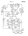
- Fig. 6 shows a circuit configuration of a third embodiment of this invention.
- the same reference numerals designate the same parts in Fig. 2 and the detailed description thereof is omitted.
- the constant current supplying circuit 21 is controlled by the control signal generating circuit 31, and the value of the second input digital signal supplied to the comparator 33 of the control signal generating circuit 31, the pulse width W N (refer to F ig. 3D) of the control signal S 4 derived from the control signal generating circuit 31 and the value of a current I outputted from the constant current supplying circuit 21 have a relationship as shown in the following table:
- the maximum value of the pulse width W N of the control signal S 4 generated from the control signal generating circuit 31 can be made small and hence, the sampling frequency can be increased, and due to the decrease of an IC clock number the IC production becomes easy.
- Fig. 7 shows a circuit configuration of a fourth embodiment of the invention.
- the same reference numerals designate the same parts in Fig. 2 and the detailed description thereof is omitted.
- the clock generator 42 generating the clock signals S 7 and S 8 is controlled by the control signal S 4 derived from the control signal generating circuit 31, and the value of the second digital input signal supplied to the comparator 33 is set in correspondence to the frequency of the clock signals S 7 and S 8 from the clock generator 42, whereby it is possible to generate a number of the pulse signals proportional to the value of the second input digital signal.
- the control signal S 4 is supplied to the clock generator 42 and the control signal S 5 to the AND circuits 40 and 41. Therefore, the AND circuit 39 is not necessary, to thereby simplify the circuit configuration of the present embodiment.
- the absolute value of at least one of the first and second input digital signals may be determined as 2 n (n - 0, l, 2, ...), which is used for a floating-point calculation.
- a plurality of circuit configurations constructed by all the circuit components other than the integration circuit 26 may be connected to the integration circuit 26, wherein if it is assumed that there are N circuits connected to the integration circuit, is obtained.
- Vout is an analog output signal
- DI ln represents the first digital input signal supplied to the nth multiplication circuit (corresponding to the circuit constructed by all the circuit components other than the integration circuit 26)
- DI 2n the second input digital signal supplied to the nth multiplication circuit.
- a plurality of the control signal generating circuits 28 may be provided. Assuming that there are provided N control signal generating circuits, is obtained.
- DI n represents the first digital input signal supplied to the nth control signal generating circuit 28.
- each of the aforementioned embodiments may be provided with two constant current supplying circuits of a different value as the constant current circuit 21 to form a continually integrating D/A converter, wherein upper bits of the first digital input signal are converted by the use of the current supplying circuit having a larger current value or both of the current supplying circuits, and lower bits of the first digital input signal is converted by the use of the current supplying circuit having a smaller current value.
- This embodiment has an advantage of lowering the clock frequency.
- the switched capacitor arranged between the integration circuit and the constant current supplying circuit is controlled in response to the values of the first and second digital input signals, so that an analog output corresponding to a product of a plurality of input digital signals can be generated by only one D/A converter, whereby the configuration of the circuit is simplified and the producion cost is reduced.
Landscapes
- Engineering & Computer Science (AREA)
- Theoretical Computer Science (AREA)
- Physics & Mathematics (AREA)
- Computer Hardware Design (AREA)
- Mathematical Physics (AREA)
- Automation & Control Theory (AREA)
- Evolutionary Computation (AREA)
- Fuzzy Systems (AREA)
- General Physics & Mathematics (AREA)
- Software Systems (AREA)
- Analogue/Digital Conversion (AREA)
Abstract
Applications Claiming Priority (2)
| Application Number | Priority Date | Filing Date | Title |
|---|---|---|---|
| JP60098559A JPS61256826A (ja) | 1985-05-09 | 1985-05-09 | D/aコンバ−タ |
| JP98559/85 | 1985-05-09 |
Publications (3)
| Publication Number | Publication Date |
|---|---|
| EP0222021A1 true EP0222021A1 (fr) | 1987-05-20 |
| EP0222021A4 EP0222021A4 (en) | 1990-12-27 |
| EP0222021B1 EP0222021B1 (fr) | 1993-03-17 |
Family
ID=14223042
Family Applications (1)
| Application Number | Title | Priority Date | Filing Date |
|---|---|---|---|
| EP86902912A Expired - Lifetime EP0222021B1 (fr) | 1985-05-09 | 1986-05-09 | Convertisseur numerique/analogique |
Country Status (7)
| Country | Link |
|---|---|
| US (1) | US4851844A (fr) |
| EP (1) | EP0222021B1 (fr) |
| JP (1) | JPS61256826A (fr) |
| KR (1) | KR940002811B1 (fr) |
| AU (1) | AU590171B2 (fr) |
| DE (1) | DE3688039T2 (fr) |
| WO (1) | WO1986006896A1 (fr) |
Families Citing this family (6)
| Publication number | Priority date | Publication date | Assignee | Title |
|---|---|---|---|---|
| JP2674648B2 (ja) * | 1987-08-03 | 1997-11-12 | 株式会社日立製作所 | パルス幅変調信号発生装置 |
| JPH02502687A (ja) * | 1987-08-25 | 1990-08-23 | ベロルススキー、ゴスダルストベンヌイ、ユニベルシテート、イメーニ、ベー.イー.レーニナ | 数‐パルス継続時間コンバータ |
| GB8813162D0 (en) * | 1988-06-03 | 1988-07-06 | British Telecomm | Digital-to-analogue conversion |
| JP3758849B2 (ja) * | 1998-04-28 | 2006-03-22 | ローム株式会社 | データ変換装置 |
| JP4041260B2 (ja) * | 2000-03-02 | 2008-01-30 | 日本電子株式会社 | 荷電粒子ビーム装置及び荷電粒子ビーム装置の制御方法 |
| US6476747B1 (en) * | 2001-04-10 | 2002-11-05 | Adc Telecommunications Israel Ltd. | Digital to analog converter |
Family Cites Families (7)
| Publication number | Priority date | Publication date | Assignee | Title |
|---|---|---|---|---|
| US2018066A (en) * | 1935-03-07 | 1935-10-22 | Universal Oil Prod Co | Treatment of hydrocarbon oils |
| US3422423A (en) * | 1965-01-04 | 1969-01-14 | Sperry Rand Corp | Digital-to-analog converter |
| US4205303A (en) * | 1978-03-31 | 1980-05-27 | International Business Machines Corporation | Performing arithmetic using indirect digital-to-analog conversion |
| JPS5938768B2 (ja) * | 1979-07-27 | 1984-09-19 | 日本電信電話株式会社 | 復号化回路 |
| AU545014B2 (en) * | 1980-02-15 | 1985-06-27 | Sony Corporation | D/a converter |
| JPS58115925A (ja) * | 1981-12-29 | 1983-07-09 | Pioneer Electronic Corp | D/a変換器 |
| JP2969396B2 (ja) * | 1991-07-25 | 1999-11-02 | 京セラ株式会社 | 調光機能を有するフラッシュ装置 |
-
1985
- 1985-05-09 JP JP60098559A patent/JPS61256826A/ja active Pending
-
1986
- 1986-05-09 WO PCT/JP1986/000240 patent/WO1986006896A1/fr not_active Ceased
- 1986-05-09 KR KR1019870700005A patent/KR940002811B1/ko not_active Expired - Fee Related
- 1986-05-09 AU AU58677/86A patent/AU590171B2/en not_active Ceased
- 1986-05-09 EP EP86902912A patent/EP0222021B1/fr not_active Expired - Lifetime
- 1986-05-09 DE DE86902912T patent/DE3688039T2/de not_active Expired - Fee Related
- 1986-05-09 US US07/026,578 patent/US4851844A/en not_active Expired - Lifetime
Also Published As
| Publication number | Publication date |
|---|---|
| EP0222021A4 (en) | 1990-12-27 |
| US4851844A (en) | 1989-07-25 |
| EP0222021B1 (fr) | 1993-03-17 |
| KR880700551A (ko) | 1988-03-15 |
| DE3688039D1 (de) | 1993-04-22 |
| WO1986006896A1 (fr) | 1986-11-20 |
| AU5867786A (en) | 1986-12-04 |
| KR940002811B1 (ko) | 1994-04-02 |
| AU590171B2 (en) | 1989-10-26 |
| DE3688039T2 (de) | 1993-09-30 |
| JPS61256826A (ja) | 1986-11-14 |
Similar Documents
| Publication | Publication Date | Title |
|---|---|---|
| EP0227871A1 (fr) | Convertisseur numérique-analogique parallèle algorithmique | |
| EP0104999B1 (fr) | Dispositif pour changer de gain, avec erreur diminuée, pour un wattmètre | |
| US4034364A (en) | Analog-digital converter | |
| US5373292A (en) | Integration type D-A/A-D Conversion apparatus capable of shortening conversion processing time | |
| US4851844A (en) | D/A converter with switched capacitor control | |
| US4684924A (en) | Analog/digital converter using remainder signals | |
| US5889424A (en) | Pulse width modulation operation circuit | |
| US5144310A (en) | A/D converter utilizing successive approximation | |
| US5182561A (en) | Integrated converter with gate for supplying integrating dock pulses to counters only during reference signal integrating period | |
| US6157672A (en) | Pulse modulation operation circuit | |
| US4864304A (en) | Analog voltage signal comparator circuit | |
| RU2145149C1 (ru) | Сигма-дельта-аналого-цифровой преобразователь | |
| SU1211886A2 (ru) | Интегрирующий аналого-цифровой преобразователь | |
| SU690624A1 (ru) | Цифро-аналоговый преобразователь | |
| SU594582A1 (ru) | Функциональный аналого-цифровой преобразователь | |
| SU974569A1 (ru) | Преобразователь кода в импульсы ступенчатой формы | |
| SU738156A1 (ru) | Преобразователь напр жени в частоту следовани импульсов | |
| SU879765A1 (ru) | Способ аналого-цифрового преобразовани | |
| JP2651240B2 (ja) | A/d変換器 | |
| SU1372621A1 (ru) | Аналого-цифровой преобразователь | |
| RU2052891C1 (ru) | Генератор пилообразного напряжения | |
| JPH0621816A (ja) | D/aコンバータテスト回路 | |
| SU1332334A1 (ru) | Устройство дл оценки плотности веро тности случайного сигнала | |
| SU1332530A1 (ru) | Устройство дл измерени времени установлени выходного напр жени цифроаналоговых преобразователей | |
| EP0099203A2 (fr) | Circuits d'extraction de racine carrée |
Legal Events
| Date | Code | Title | Description |
|---|---|---|---|
| PUAI | Public reference made under article 153(3) epc to a published international application that has entered the european phase |
Free format text: ORIGINAL CODE: 0009012 |
|
| AK | Designated contracting states |
Kind code of ref document: A1 Designated state(s): DE FR GB NL |
|
| 17P | Request for examination filed |
Effective date: 19870519 |
|
| A4 | Supplementary search report drawn up and despatched |
Effective date: 19901106 |
|
| AK | Designated contracting states |
Kind code of ref document: A4 Designated state(s): DE FR GB NL |
|
| 17Q | First examination report despatched |
Effective date: 19910828 |
|
| GRAA | (expected) grant |
Free format text: ORIGINAL CODE: 0009210 |
|
| AK | Designated contracting states |
Kind code of ref document: B1 Designated state(s): DE FR GB NL |
|
| REF | Corresponds to: |
Ref document number: 3688039 Country of ref document: DE Date of ref document: 19930422 |
|
| ET | Fr: translation filed | ||
| PLBE | No opposition filed within time limit |
Free format text: ORIGINAL CODE: 0009261 |
|
| STAA | Information on the status of an ep patent application or granted ep patent |
Free format text: STATUS: NO OPPOSITION FILED WITHIN TIME LIMIT |
|
| 26N | No opposition filed | ||
| REG | Reference to a national code |
Ref country code: GB Ref legal event code: IF02 |
|
| PGFP | Annual fee paid to national office [announced via postgrant information from national office to epo] |
Ref country code: GB Payment date: 20030507 Year of fee payment: 18 |
|
| PGFP | Annual fee paid to national office [announced via postgrant information from national office to epo] |
Ref country code: FR Payment date: 20030508 Year of fee payment: 18 |
|
| PGFP | Annual fee paid to national office [announced via postgrant information from national office to epo] |
Ref country code: DE Payment date: 20030522 Year of fee payment: 18 |
|
| PGFP | Annual fee paid to national office [announced via postgrant information from national office to epo] |
Ref country code: NL Payment date: 20030530 Year of fee payment: 18 |
|
| PG25 | Lapsed in a contracting state [announced via postgrant information from national office to epo] |
Ref country code: GB Free format text: LAPSE BECAUSE OF NON-PAYMENT OF DUE FEES Effective date: 20040509 |
|
| PG25 | Lapsed in a contracting state [announced via postgrant information from national office to epo] |
Ref country code: NL Free format text: LAPSE BECAUSE OF NON-PAYMENT OF DUE FEES Effective date: 20041201 Ref country code: DE Free format text: LAPSE BECAUSE OF NON-PAYMENT OF DUE FEES Effective date: 20041201 |
|
| GBPC | Gb: european patent ceased through non-payment of renewal fee |
Effective date: 20040509 |
|
| PG25 | Lapsed in a contracting state [announced via postgrant information from national office to epo] |
Ref country code: FR Free format text: LAPSE BECAUSE OF NON-PAYMENT OF DUE FEES Effective date: 20050131 |
|
| NLV4 | Nl: lapsed or anulled due to non-payment of the annual fee |
Effective date: 20041201 |
|
| REG | Reference to a national code |
Ref country code: FR Ref legal event code: ST |