EP0222345A1 - Méthod de test d'un circuit imprimé - Google Patents
Méthod de test d'un circuit imprimé Download PDFInfo
- Publication number
- EP0222345A1 EP0222345A1 EP86115465A EP86115465A EP0222345A1 EP 0222345 A1 EP0222345 A1 EP 0222345A1 EP 86115465 A EP86115465 A EP 86115465A EP 86115465 A EP86115465 A EP 86115465A EP 0222345 A1 EP0222345 A1 EP 0222345A1
- Authority
- EP
- European Patent Office
- Prior art keywords
- guide plate
- adapter
- guide
- grid
- circuit board
- Prior art date
- Legal status (The legal status is an assumption and is not a legal conclusion. Google has not performed a legal analysis and makes no representation as to the accuracy of the status listed.)
- Granted
Links
- 238000012360 testing method Methods 0.000 title claims abstract description 60
- 238000000034 method Methods 0.000 title claims description 7
- 238000003780 insertion Methods 0.000 claims description 10
- 230000037431 insertion Effects 0.000 claims description 10
- 230000007547 defect Effects 0.000 claims description 6
- 230000003287 optical effect Effects 0.000 claims description 4
- 238000006073 displacement reaction Methods 0.000 abstract 1
- 238000013461 design Methods 0.000 description 11
- 238000005553 drilling Methods 0.000 description 5
- VVQNEPGJFQJSBK-UHFFFAOYSA-N Methyl methacrylate Chemical compound COC(=O)C(C)=C VVQNEPGJFQJSBK-UHFFFAOYSA-N 0.000 description 3
- 229920005372 Plexiglas® Polymers 0.000 description 3
- 230000002950 deficient Effects 0.000 description 3
- 230000015572 biosynthetic process Effects 0.000 description 2
- 238000006243 chemical reaction Methods 0.000 description 2
- 238000011161 development Methods 0.000 description 2
- 230000018109 developmental process Effects 0.000 description 2
- 239000003822 epoxy resin Substances 0.000 description 2
- 239000004033 plastic Substances 0.000 description 2
- 229920003023 plastic Polymers 0.000 description 2
- 229920000647 polyepoxide Polymers 0.000 description 2
- 238000003756 stirring Methods 0.000 description 2
- 230000005540 biological transmission Effects 0.000 description 1
- 238000010276 construction Methods 0.000 description 1
- 238000001514 detection method Methods 0.000 description 1
- 239000011152 fibreglass Substances 0.000 description 1
- 239000011521 glass Substances 0.000 description 1
- 239000003365 glass fiber Substances 0.000 description 1
- 239000000463 material Substances 0.000 description 1
- 239000011159 matrix material Substances 0.000 description 1
- 238000004382 potting Methods 0.000 description 1
- 230000003014 reinforcing effect Effects 0.000 description 1
- 238000007665 sagging Methods 0.000 description 1
- 238000012549 training Methods 0.000 description 1
- 238000002834 transmittance Methods 0.000 description 1
- 239000012780 transparent material Substances 0.000 description 1
Images


Classifications
-
- G—PHYSICS
- G01—MEASURING; TESTING
- G01R—MEASURING ELECTRIC VARIABLES; MEASURING MAGNETIC VARIABLES
- G01R1/00—Details of instruments or arrangements of the types included in groups G01R5/00 - G01R13/00 and G01R31/00
- G01R1/02—General constructional details
- G01R1/06—Measuring leads; Measuring probes
- G01R1/067—Measuring probes
- G01R1/073—Multiple probes
- G01R1/07307—Multiple probes with individual probe elements, e.g. needles, cantilever beams or bump contacts, fixed in relation to each other, e.g. bed of nails fixture or probe card
- G01R1/07364—Multiple probes with individual probe elements, e.g. needles, cantilever beams or bump contacts, fixed in relation to each other, e.g. bed of nails fixture or probe card with provisions for altering position, number or connection of probe tips; Adapting to differences in pitch
- G01R1/07371—Multiple probes with individual probe elements, e.g. needles, cantilever beams or bump contacts, fixed in relation to each other, e.g. bed of nails fixture or probe card with provisions for altering position, number or connection of probe tips; Adapting to differences in pitch using an intermediate card or back card with apertures through which the probes pass
Definitions
- the invention relates to an adapter according to the preamble of claim 1.
- an adapter of this type is the subject of an older proposal by the applicant, which includes equipping such an adapter for both machine and manual assembly of the adapter.
- the adapter is assigned a special alignment device for the adapter pins, which limits their deflection movements when the adapter pins are inserted into the guide holes.
- the adapter is assigned an optically effective auxiliary device, by means of which the insertion of the adapter pins is facilitated.
- the adapter pins For adapters of the present type, there is a requirement that the adapter pins must not touch each other to avoid short circuits. With the given grid dimensions and necessary dimensions for the adapter pins, for the guide hole diameter and for the thickness of the guide plates and the distance between them, the aforementioned requirement is not easy to meet. It should be taken into account that the adapter pins should be insertable as easily as possible.
- the invention has for its object to design an adapter of the type described in such a way that the mutual contact of adapter pins is excluded and the adapter pins are easy to move.
- the special limitation of the pin deflection angle ensures that an adapter pin cannot be inserted at all in the position in which it could touch another adapter pin.
- one of these two adapter pins would have to be inserted into a guide hole in the second guide plate, which is offset by a larger amount from the assigned raster point than is predetermined by the maximum pin deflection angle.
- the adapter pin in question cannot therefore be inserted into such a guide hole.
- the configuration according to the invention is the same can be used advantageously for both mechanical and manual fitting of an adapter with adapter pins.
- the configuration according to the invention also considerably simplifies the adapter and facilitates the insertion of the adapter pins.
- the simplification is that the first guide plate has guide holes at all grid points and is therefore the same for all adapters.
- the transparent design of the first guide plate according to claim 2 facilitates the insertion of the adapter pins in manual assembly because the operator can visually recognize the guide holes in the second guide plate into which the adapter pins are to be inserted. Due to the transparent, namely transparent or almost transparent design of the first guide plate, the contact holes in the second guide plate are clearly visible. Visibility is improved by the fact that in the assembly position the guide plates are at a relatively small distance from one another which is to be coordinated with the design parameters according to the invention.
- the embodiment according to claim 3 relates to the assignment of a special guide between the first and the second stirring plate, through which the change in distance can be easily implemented.
- the first guide plate or the second guide plate or both guide plates can be adjusted simultaneously.
- a change in distance between the guide plates can also be facilitated by assigning an adjustment mechanism.
- Such a mechanism is recommended, which the guide plate or the guide plates in the end positions.
- Spindle drives or cylinder-piston drives represent usable adjustment drives.
- the solution contained in claim 5 also solves the problem on which the invention is based and thus presents itself as a solution independent of the solution contained in claim 1.
- each required adapter pin is assigned a positive guide, which results in only one insertion option for each adapter pin, i.e. the adapter is reproducible to 10DX.
- each adapter pin inserted into a guide hole of the first guide plate can only be inserted into the guide hole in the third guide plate assigned to the respective guide hole in the third guide plate, which is in alignment with the associated guide holes in the first guide plate and in the second guide plate.
- the movement of the relevant adapter pin in the guide hole of the first guide plate and the distance between the first guide plate and the third guide plate and the size of the associated guide hole in the third guide plate are coordinated so that the insertion end of the adapter pin within the edge of the guide hole in the third guide plate immersed in the latter and in the associated guide hole in the second guide plate.
- Advantageous are tapered adapter pins on their insertion ends, the arrangement is such that the pen tips are at the maximum pin deflection angle within the hole edges of the guide holes in the third and in the second guide plate.
- the adapter can be filled particularly easily.
- guide holes need only be drilled in the first guide plate in such a number that corresponds to the number of test points on the circuit board, i.e. corresponds to the number of guide holes in the second guide plate.
- the first guide plate does not need to be made of transparent material, e.g. Plexiglass. It can advantageously consist of an epoxy resin-based plastic, in particular reinforced by glass fibers, which is much easier to drill than e.g. Plexiglass.
- the reinforcing insert in the third guide plate is important because it reduces the sagging of the guide plates in the case of large guide plates.
- the degree of offset with which a guide hole in the third guide plate is offset from the raster point assigned to it is determined by the ratio of the distances between the first guide plate and the third guide plate and the distance between the third guide plate and the second guide plate.
- the pin deflection angle results from the guide play of the adapter pin in the first guide plate, the pin diameter, the guide hole diameter and the guide hole length having an influence.
- a large pin deflection angle inevitably results in a large swivel circle in the area of the third guide plate.
- the design according to claim 6 is advantageous because, due to the necessary movement play of the adapter pin in the first guide plate, the deflection circle that can be described by the introducer of the adapter pin is relatively small, so that with relatively little movement play in the guide hole of the third guide plate, blockages during insertion of the adapter pin by hitting the free adapter pin ends on the hole edge of the guide hole in the third guide plate are avoided and, due to the relatively small amount of play in the third guide plate, an impact on the hole edge of the guide hole in the second guide plate is also avoided.
- a balanced ratio of the distances between the third guide plate and the first guide plate and the second guide plate is given when the distance between the second guide plate and the third guide plate is approximately 80% of the distance between the first guide plate and the second guide plate.
- the insertion of the adapter pins can be observed from below due to the light transmission. This is possible because the end of the adapter pin in question can be recognized either directly or as a silhouette. As a result, the adapter pin can be controlled and can therefore be inserted specifically into the guide hole assigned to it.
- the light does not have to be arranged above the adapter pin, because even a lateral light source casts a shadow on the lower guide plate from the adapter pin in question, which emanates from the tip of the adapter pin.
- the control with regard to the viewing position is simplified by a mirror arranged according to claim 8.
- the adapter pins are given a limited all-round clearance due to the enlarged guide holes in the middle guide plate, which allows the adapter pins to be moved back and forth, the greatest deflection dimension being able to be predetermined by the size of the guide holes in this guide plate .
- the freedom of movement of the adapter pins can be limited to the guide holes closest to the adapter pin tips to be inserted. This restriction prevents the adapter pin tip in question from being inserted into a distant guide hole.
- the embodiment according to claim 12 makes it possible to change the aforementioned all-round scope for the adapter pins, for example in accordance with the existing grid size. This is possible by moving the middle guide plate. The further the middle guide plate is pushed towards the upper guide plate, the greater this conical clearance in which the adapter pins can be guided back and forth. If this scope is to be restricted, the middle guide plate should be moved towards the lower guide plate, i.e. removed from the upper guide plate.
- position-independent lighting in the sense of a hand lamp is proposed, which enables the lighting to be carried out in a targeted manner so that the desired shadow formation on the lower guide plate can be optimally generated.
- the adapter Since the adapter is a self-contained component, it is advisable to attach the mirror to a frame on which the adapter can be placed for the purpose of the lunar days of the adapter pins.
- the mirror is inclined towards the front or back of the adapter in relation to the lower guide plate, the mirror image can be read more easily. If necessary, this design also makes it easier to transmit the mirror image by means of a mirror device comprising two mirrors, e.g. in the eye level of the operator.
- the invention further relates to an adapter according to the preamble of claim 15.
- the task is to dimension individual parts of the adapter so that simple charging is ensured in a short time, the charging yield should be as 100% as possible. This means that it is no longer necessary to reload individual holes by hand.
- the adapter is said to be particularly suitable for charging with an automatic charging system, as described in DE-OS 33 40 184 by the applicant.
- the invention further relates to a method for Display of defects on a circuit board to be tested with test points located in and / or outside the grid using an adapter according to one of claims 15 to 18.
- This method is intended to be a particularly simple direct display of the sources of errors or a simple search for the defects on the defective circuit board enable. The features necessary for this are the subject of claim 19.
- a computer used to calculate the drilling pattern for the guide plates of the adapter can additionally be used for the data or coordinates of the test contacts determined by the circuit board tester, the faulty test points located in and / or outside the grid correspond to the circuit board to be tested, convert it into the data or coordinates of the last-mentioned test points so that they can either be located on the circuit board or marked directly optically. This conversion is necessary because the circuit board tester can only determine the data or coordinates of the test contacts mentioned, which are on the side of the first guide plate of the adapter, ie are in a grid.
- This optical search system can function, for example, like a conventional drawing machine, in which the two coordinates of the respective position of the drawing head are displayed.
- the drawing head equipped with a magnifying glass system with crosshairs can then be moved into the position that corresponds to the determined coordinates.
- a mounting plate of the device (not shown) for testing printed circuit boards is designated by 1.
- the test contacts 7 carry telescopically retractable and extendable test contact heads 8 which are biased towards their outer end position by a spring, not shown.
- test contacts 7 are fastened in the modules 6 by potting and are connected by electrical lines 9 to circuit boards 12 carrying IC chips 11, which are arranged within the modules 6 and in their entirety to the circuit boards 12, the IC chips 11 and if necessary, other components form a partial switch matrix assigned to the test contacts 7.
- a raster adapter 13 which has a plurality of adapter pins 14 which pass through it and which connect the test contacts 7 arranged in the raster to the test points 3 arranged outside the raster.
- the adapter pins 14 are therefore not in the respective alignment with the test contacts, but extend obliquely through the adapter 13, with both ends protruding from the adapter and forming raised contact points with respect to the top and bottom.
- the structure of the adapter 13 can be seen from FIG.
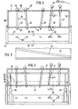
- the adapter 13 consists of a lower guide plate 15 with guide holes 16 arranged in the pattern of the test points of the circuit board 2 to be tested, which is not shown in FIG. 2, and an upper guide plate 17 spaced above and parallel to this, with guide holes 18 arranged in a grid for the adapter pins 14.
- the guide plate 15 and the guide plate 17 form a box shape with end plates 19 fastened to them on the end face.
- the adapter pins 14 can be inserted from above through the guide holes 16, 18 and they have ball heads 21 at their upper ends, which in the fully inserted position on the edges 22 of the guide holes 18 rest.
- Five adapter pins 23 to 27 are shown, of which the adapter pins 23 to 25 are fully inserted, while the adapter pins 26 and 27 stand on the guide plate 15. While the guide holes 16, 18 for the adapter pins 23 and 26 are aligned with one another, that is to say they lie in a grid, the guide holes 16, 18 for the adapter pins 24, 25 and 27 do not align with one another because these guide holes in the guide plate 15 are out of grid, as a result of which an inclination of the fully inserted adapter pins 24, 25 and 27 is required.
- the adapter 13 is located on a mounting frame 31 for the purpose of inserting the adapter pins 23 to 27, which are inserted by hand.
- a mirror 32 is attached in the mounting frame 31, which is inclined to the front of the adapter 13, ie to the side on which the operator stands.
- the guide plate 17 consists of a plastic, which is not transparent, but allows a certain amount of light to pass through, so that the guide plate 15 is also illuminated by the light rays of the hand lamp 33.
- the guide plate 15 also consists of a material which is slightly translucent, the shadow cast by the adapter pins 26, 27 on the guide plate 15 is visible from below. Therefore, not only the guide holes 16 of the guide plate 15, but also the shadows designated by 34 appear on the mirror 32. Based on this shadow image, the operator can see on which side of the guide hole 16 in question the relevant adapter pin tip is located. By appropriate steering Movements of the adapter pins 26, 27, which are brought about by manual intervention on the ball heads 21, can be introduced into the associated guide holes 16 in a targeted manner.
- the deflection dimension designated a is determined by the diameter d of the contact holes 18, which are gripped by the adapter pins 14 with a certain amount of play.
- a central guide plate 35 is arranged between the guide plate 15 and the guide plate 17, parallel to the latter, which is vertically adjustable with the aid of two piston cylinders 36, the piston rods 37 of which engage the contact plate 15 in holes 38 between a lower, dash-dotted position, which is limited by stops 39, and an upper position, shown with solid lines.
- the middle stirring plate 35 has guide holes 41, the diameter D of which is larger than the diameter d of the adapter pins 14.
- the deflection dimension a is determined in this case by the size of the guide holes 41.
- the adapter designated 45 also has a box construction. It consists of a first guide plate 46 with guide holes 47 at all grid points and a second guide plate 48 with guide holes 49, in the pattern of the test points of the circuit board to be tested.
- the first guide plate 47 is transparent and, in a preferred embodiment, is made of plexiglass.
- the second guide plate 48 does not need to be transparent and, in a preferred embodiment, consists of a glass fiber-reinforced plastic based on epoxy resin, which is referred to in technical jargon as EPG.
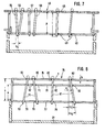
- guides 52 are formed in the form of guide slots, in which the second guide plate 48 vertically between a mounting position shown in FIG. 5 and one shown in FIG. 7 for the purpose of changing the distance between the guide plates 46, 48 Working position is adjustable.
- a mechanism which is indicated in FIG. 5 as a spindle drive 53 or cylinder-piston drive 54, can serve to adjust the second guide plate 48.
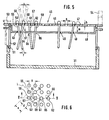
- Fig. 5 shows the guide plates 46, 48 and the adapter pins 55 to 58 in a section along the line VV in Fig. 6, which shows a corresponding section of Fig. 5 in plan view.
- the adapter pins 55 to 58 are inserted from above through the guide holes labeled 59 to 62 in the first guide plate 46 and the guide holes labeled 63 to 66 in the second guide plate 48.
- the one labeled 64 is at a maximum distance d from it assigned grid point, namely the guide hole 60 removed.
- the guide holes 63, 65 and 66 in the second guide plate 48 have a smaller distance from the grid points assigned to them, namely guide holes 59, 61 and 62 in the first guide plate 46.
- the distance d is half the diagonal dimension e from the guide holes arranged in a square 47 in the first guide plate 46, the pitch of which is denoted by R.
- the diameter f of the adapter pins, the diameter g of the guide holes 47 in the first guide plate 46 and the thickness h of the first guide plate 46 are coordinated with one another in such a way that the tips 67 of the adapter pins 55 describe a wobble circle 68 when one with its tip 67 adapter pin lying on the second guide plate 48 is moved in the sense of a wobble movement, as shown in FIG. 5 is indicated by dash-dotted lines.
- the dimensions described above are coordinated with one another in such a way that the maximum radius of the wobble circle 68 corresponds to half of the diagonal dimension e and thus the distance d.
- the guide hole 64 in the second guide plate 48 has the special feature that it lies on the diagonal i. As a result, it has an equal distance d from the guide holes labeled 59.60 and 69.70. That is, the adapter pin 56, which is just a little stiff to insert through the guide hole 60 into the guide hole 64 due to the aforementioned dimensions, could also just be stiffly inserted into the guide hole 64 by each of the guide holes 59 and 69 and 70.
- the assembly of such holes 64 in the second guide plate 48 which lie at the intersection of diagonals i, which pass through guide holes 59, 60, 69, 70 arranged in a square, is thus 4 times indefinite.
- the pin deflection angle which the adapter pins assume with respect to the vertical, is designated k 1 in the mounting position according to FIG. 5, regardless of its size. Moving the second guide plate 48 into the working position shown in FIG. 7 reduces the pin deflection angle. The reduced angles are designated k 2 in FIG. 7. This ensures the smooth running of the adapter pins, in particular the adapter pins that are inserted into guide holes 64 that lie at the intersection of diagonals i. A mutual contact of adapter pins 55 to 58 is excluded by pulling the guide plates 46, 48 apart because the adapter pins 55 to 58 move away from one another.
- the adapter designated here 75 has an upper first guide plate 76, a lower second guide plate 77 and a third guide plate 78 arranged between them.
- the third guide plate 78 is rigidly arranged here. It could be variable in distance, but only for the purpose of its basic positioning. A change in the distance for each assembly is not provided.
- the adapter 75 of this embodiment is 100% reproducible. This means that the placement of guide holes 79 lying outside the grid in the second guide plate 77 must not be indefinite. In other words, each guide hole 79 in the second plate 77 is assigned a very specific guide hole 80 in the first guide plate 76 for the assembly.
- the guide holes 80 in the first guide plate 76 are arranged in a grid. In contrast to the embodiment according to FIGS. 5 to 7, however, not at all grid points, but only at those which are to accommodate 75 adapter pins 81 for equipping the special adapter.
- the third guide plate 78 is provided with guide holes 82 which can lie in and outside the grid.
- the guide holes 82 in the third guide plate 78 lying outside of the grid are less offset from the nearest guide holes 80 in the grid of the first guide plate 76 (v 1 ) than the corresponding guide holes 79 in the second guide plate 77 (v 2 ).
- the offset v 1 of the guide holes 82 lying outside the grid in the third guide plate 78 is selected such that - if the offset v 1 is a maximum - the cone-shaped tip 83 of the adapter pins 81 in each case is still in the guide holes 79 of the second guide plate 77 is immersed, regardless of the pin deflection angle k 3, the adapter pins 81 are inserted into the first guide plate 76.
- the offset v 3 of the off-grid guide holes 82 in the third guide plate 78 is determined in the knowledge of the offset v 2 of the off-grid guide holes 79 in the second guide plate 77, for example calculated by a computer.
- the thickness h of the first guide plate 76 and the play s of the adapter pins 81 in the guide holes 80 and the play 51 in the guide holes 82 of the third guide plate 78 are similar in the embodiment according to FIG matched to one another so that the possibly pointed tips 83 of the adapter pins 81 dip into the guide holes 82 when inserted.
- the adapter pins have a cylindrical shaft, a spherical head and a preferably conical tip.
- the pin length 1 is approximately larger by the size of the spherical head than the transverse dimension p of the adapter.
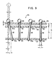
- FIG. 9 also shows an adapter consisting of a first guide plate 176, a second guide plate 177 and a third guide plate 178 arranged in between.
- the third guide plate 178 also has grid holes 182 and grid holes 182a out of grid.
- the offset of the off-grid guide holes 182a in the third guide plate relative to the corresponding guide holes 180 in the first guide plate 176 is selected here so that when an adapter pin 181 is inserted vertically into a guide hole 180 of the first guide plate 176, it is ensured that the conical one Tip of the adapter pin 181 still in the corresponding out of grid guide hole 182a of the third guide plate 178, and on the other hand - if the adapter pin 189 is continued through the guide hole 182 - this adapter pin 181 is inevitably guided into the corresponding out of grid guide hole 179a. In this way, in particular when using an automatic loading system according to DE-OS 33 40 184, a practically 100% yield during charging is ensured within a very short time. It is important here that the adapter pins 181 can always be inserted vertically into the guide holes 180 of the first guide plate, regardless of whether the guide holes in the second guide plate 177 are in a grid or out of grid.
- the position of the guide holes 180 of the first guide plate 176 are predetermined by the grid.
- the position of the guide holes 179, 179a in the second guide plate 177 is predetermined by the hole pattern of the circuit board to be tested.
- the offset of the guide holes 182a in the third guide plate 178 can be calculated taking into account the aforementioned conditions and position data, for which a computer (computer) is particularly suitable.
- the plate diameter S, the pin diameter D, the hole diameter L and the distances between the guide plates Al, A2 and A3 so selected must, that the above-mentioned desired condition can always be realized, that is, even if the offset V 2 between a guide hole 180 in the first guide plate 176 and a guide hole 179a in the second guide plate 177 is maximum in terms of the reproducibility of an adapter charge image.
- the process sequence shown in FIG. 10 for displaying defects on a circuit board to be tested is as follows: based on a pattern board 190 corresponding to a circuit board 198 to be tested, a hole pattern is entered into a computer 191.
- the one Data corresponding to the hole pattern can be stored on a data carrier, for example a disk 192. It is also possible to retrieve the data from the data carrier 192 and enter it into the computer 191.
- the computer 191 now calculates the hole pattern for the holes in the guide plates of the adapter according to FIG. 9.
- the data or coordinates for this drilling pattern are input into an NC drilling machine 193, by means of which the three guide plates 176, 177, and 178 are drilled. After drilling, the guide plates are assembled to the (still unloaded) adapter 175.
- the circuit board tester determines the data or coordinates of those test contacts that rest on the ball heads of the adapter pins.
- the test contacts are on the side of the first guide plate 176, that is, all in the grid. These test contacts are connected via the adapter pins to defective holes in the circuit board 198 to be tested.
- the faulty holes of the circuit board 198 to be tested are to be displayed. However, some of these are out of grid, ie they are on the side of the second guide plate 177.
- the Data or coordinates of the test contacts located in the grid determined by the circuit board testing device 197 are in turn fed to the computer 191.
- the computer 191 accordingly outputs to an error display device 195 the data or coordinates of the defective test points of the circuit board 198 to be tested, which correspond to the error coordinates or data of the holes in the second guide plate 177.
- These data or coordinates are displayed on a monitor 196 and can be used by an operator using an optical search device with a coordinate display to find the faulty test points on the circuit board 198 to be tested.
- error display device 195 it is also possible to design the error display device 195 in such a way that it directly displays faulty test points or holes on the printed circuit board 198 to be tested, for example by means of a light point which is generated by a projector head which can be moved in two coordinate directions.
Landscapes
- Physics & Mathematics (AREA)
- General Physics & Mathematics (AREA)
- Tests Of Electronic Circuits (AREA)
- Testing Of Short-Circuits, Discontinuities, Leakage, Or Incorrect Line Connections (AREA)
- Measuring Leads Or Probes (AREA)
Priority Applications (1)
| Application Number | Priority Date | Filing Date | Title |
|---|---|---|---|
| AT86115465T ATE56277T1 (de) | 1985-11-08 | 1986-11-07 | Verfahren zur pruefung einer leiterplatte. |
Applications Claiming Priority (2)
| Application Number | Priority Date | Filing Date | Title |
|---|---|---|---|
| DE3539720 | 1985-11-08 | ||
| DE19853539720 DE3539720A1 (de) | 1985-11-08 | 1985-11-08 | Adapter fuer ein leiterplattenpruefgeraet |
Publications (2)
| Publication Number | Publication Date |
|---|---|
| EP0222345A1 true EP0222345A1 (fr) | 1987-05-20 |
| EP0222345B1 EP0222345B1 (fr) | 1990-09-05 |
Family
ID=6285516
Family Applications (1)
| Application Number | Title | Priority Date | Filing Date |
|---|---|---|---|
| EP86115465A Expired - Lifetime EP0222345B1 (fr) | 1985-11-08 | 1986-11-07 | Méthod de test d'un circuit imprimé |
Country Status (5)
| Country | Link |
|---|---|
| US (1) | US4774459A (fr) |
| EP (1) | EP0222345B1 (fr) |
| JP (1) | JPS62161066A (fr) |
| AT (1) | ATE56277T1 (fr) |
| DE (2) | DE3539720A1 (fr) |
Cited By (1)
| Publication number | Priority date | Publication date | Assignee | Title |
|---|---|---|---|---|
| EP0451690A3 (en) * | 1990-04-09 | 1993-05-26 | Atg Electronic Gmbh | Process and device for drilling and/or equipping of the guiding plates of a test adaptor |
Families Citing this family (13)
| Publication number | Priority date | Publication date | Assignee | Title |
|---|---|---|---|---|
| DE3638372A1 (de) * | 1986-11-11 | 1988-05-26 | Lang Dahlke Helmut | Vorrichtung zum pruefen von elektrischen leiterplatten |
| ATE75319T1 (de) * | 1987-11-09 | 1992-05-15 | Mania Gmbh | Adapter fuer eine vorrichtung zur elektronischen pruefung von leiterplatten. |
| EP0352929B1 (fr) * | 1988-07-26 | 1993-12-08 | Hewlett-Packard Company | Système de connection pour équipement de test de circuits imprimés |
| US5307560A (en) * | 1992-07-30 | 1994-05-03 | Allen Aksu | Automated test pin loading method |
| DE4323276A1 (de) * | 1993-07-12 | 1995-01-19 | Mania Gmbh | Vollmaterialadapter |
| IT1282689B1 (it) * | 1996-02-26 | 1998-03-31 | Circuit Line Spa | Dispositivo di conversione della griglia di punti di test di una macchina per il test elettrico di circuiti stampati non montati |
| US6407565B1 (en) | 1996-10-29 | 2002-06-18 | Agilent Technologies, Inc. | Loaded-board, guided-probe test fixture |
| US5945836A (en) | 1996-10-29 | 1999-08-31 | Hewlett-Packard Company | Loaded-board, guided-probe test fixture |
| US7059046B2 (en) * | 2002-06-24 | 2006-06-13 | Delaware Capital Formation, Inc. | Method for producing a captive wired test fixture and fixture therefor |
| US6784675B2 (en) * | 2002-06-25 | 2004-08-31 | Agilent Technologies, Inc. | Wireless test fixture adapter for printed circuit assembly tester |
| US7100273B2 (en) * | 2003-03-03 | 2006-09-05 | Hewlett-Packard Development Company, L.P. | Interconnect validation instruments |
| KR102865650B1 (ko) * | 2020-01-31 | 2025-09-29 | (주)포인트엔지니어링 | 프로브 헤드 및 이를 포함하는 프로브 카드 |
| TWI831307B (zh) * | 2022-07-26 | 2024-02-01 | 思達科技股份有限公司 | 導板結構及探針陣列 |
Citations (2)
| Publication number | Priority date | Publication date | Assignee | Title |
|---|---|---|---|---|
| EP0149776A1 (fr) * | 1983-12-08 | 1985-07-31 | Martin Maelzer | Adaptateur pour un dispositif de test de circuits imprimés |
| EP0164672A2 (fr) * | 1984-06-15 | 1985-12-18 | International Business Machines Corporation | Sonde avec un assemblage courbe multiple |
Family Cites Families (14)
| Publication number | Priority date | Publication date | Assignee | Title |
|---|---|---|---|---|
| US3654585A (en) * | 1970-03-11 | 1972-04-04 | Brooks Research And Mfg Inc | Coordinate conversion for the testing of printed circuit boards |
| US3848188A (en) * | 1973-09-10 | 1974-11-12 | Probe Rite Inc | Multiplexer control system for a multi-array test probe assembly |
| US4164704A (en) * | 1976-11-01 | 1979-08-14 | Metropolitan Circuits, Inc. | Plural probe circuit card fixture using a vacuum collapsed membrane to hold the card against the probes |
| DE2933862A1 (de) * | 1979-08-21 | 1981-03-12 | Paul Mang | Vorrichtung zur elektronischen pruefung von leiterplatten. |
| US4357062A (en) * | 1979-12-10 | 1982-11-02 | John Fluke Mfg. Co., Inc. | Universal circuit board test fixture |
| DE3013215A1 (de) * | 1980-04-03 | 1981-10-15 | Luther & Maelzer Gmbh, 3050 Wunstorf | Adapter fuer ein selbstprogrammierbares leiterplattenpruefgeraet |
| DE3110056C2 (de) * | 1981-03-16 | 1986-02-27 | MANIA Elektronik Automatisation Entwicklung und Gerätebau GmbH, 6384 Schmitten | Kontaktanordnung mit einer Vielzahl von in einer Kontaktebene angeordneten Kontakten |
| US4423376A (en) * | 1981-03-20 | 1983-12-27 | International Business Machines Corporation | Contact probe assembly having rotatable contacting probe elements |
| DE3249770C2 (en) * | 1982-11-05 | 1987-11-12 | Martin Maelzer | Device for testing electrical circuit boards |
| JPS6049270A (ja) * | 1983-08-27 | 1985-03-18 | Kyoei Sangyo Kk | プリント配線板検査機用アダプタ |
| GB2146849B (en) * | 1983-09-17 | 1987-08-05 | Marconi Instruments Ltd | Electrical test probe head assembly |
| US4535536A (en) * | 1983-11-03 | 1985-08-20 | Augat Inc. | Method of assembling adaptor for automatic testing equipment |
| DE3340180C1 (de) * | 1983-11-07 | 1985-05-15 | MANIA Elektronik Automatisation Entwicklung und Gerätebau GmbH | Kontaktfeldanordnung fuer ein rechnergesteuertes Leiterplattenpruefgeraet |
| US4686467A (en) * | 1984-03-21 | 1987-08-11 | Dit-Mco International Corp. | Circuit board testing system |
-
1985
- 1985-11-08 DE DE19853539720 patent/DE3539720A1/de not_active Withdrawn
-
1986
- 1986-11-06 US US06/927,374 patent/US4774459A/en not_active Expired - Lifetime
- 1986-11-07 DE DE8686115465T patent/DE3673953D1/de not_active Expired - Lifetime
- 1986-11-07 EP EP86115465A patent/EP0222345B1/fr not_active Expired - Lifetime
- 1986-11-07 JP JP61265424A patent/JPS62161066A/ja active Pending
- 1986-11-07 AT AT86115465T patent/ATE56277T1/de not_active IP Right Cessation
Patent Citations (2)
| Publication number | Priority date | Publication date | Assignee | Title |
|---|---|---|---|---|
| EP0149776A1 (fr) * | 1983-12-08 | 1985-07-31 | Martin Maelzer | Adaptateur pour un dispositif de test de circuits imprimés |
| EP0164672A2 (fr) * | 1984-06-15 | 1985-12-18 | International Business Machines Corporation | Sonde avec un assemblage courbe multiple |
Cited By (1)
| Publication number | Priority date | Publication date | Assignee | Title |
|---|---|---|---|---|
| EP0451690A3 (en) * | 1990-04-09 | 1993-05-26 | Atg Electronic Gmbh | Process and device for drilling and/or equipping of the guiding plates of a test adaptor |
Also Published As
| Publication number | Publication date |
|---|---|
| JPS62161066A (ja) | 1987-07-17 |
| ATE56277T1 (de) | 1990-09-15 |
| DE3539720A1 (de) | 1987-05-14 |
| EP0222345B1 (fr) | 1990-09-05 |
| DE3673953D1 (de) | 1990-10-11 |
| US4774459A (en) | 1988-09-27 |
Similar Documents
| Publication | Publication Date | Title |
|---|---|---|
| DE3519986C2 (fr) | ||
| EP0222345B1 (fr) | Méthod de test d'un circuit imprimé | |
| DE69826406T2 (de) | Rastersondenmikroskop mit Feinstellungsvorrichtung | |
| EP0350850A2 (fr) | Dispositif d'insertion de composants dans des circuits imprimés à la machine | |
| DE2826770A1 (de) | Kontaktanzeigevorrichtung fuer elektrische testgeraete | |
| DE3705749C2 (de) | Verfahren und Vorrichtung zur Ausrichtung eines Lichtemitters innerhalb seiner Packung | |
| WO2012013818A1 (fr) | Procédé et dispositif servant à calibrer une machine d'usinage au laser en utilisant un capteur de lumière laser | |
| DE2225011C3 (de) | Verfahren und Vorrichtung zum Positionieren eines Gegenstandes | |
| EP0074484B1 (fr) | Procédé et dispositif pour l'emmagasinage de points choisis d'une ligne à copier d'une machine pour le meulage de formes projetées | |
| DE3444708C2 (de) | Adapter für ein Leiterplattenprüfgerät | |
| DE3531156C1 (de) | Verfahren zum Ausrichten der Achse eines zweiten Halters in bezug auf die Achse eines ersten Halters bei einer Pruef- oder Bearbeitungsmaschine | |
| DE2944246A1 (de) | Zeichengeraet | |
| DE19805040A1 (de) | Durchlichtbeleuchtung für Koordinatenmeßmaschinen | |
| DE3340084C2 (de) | Vorrichtung zur Positionierung von Bauteilen auf einem Werkstück | |
| EP1606981A2 (fr) | Procede et dispositif d'alignement d'un substrat et d'un gabarit d'impression lors d'une impression de pate de brasage | |
| DE3144179A1 (de) | Markiervorrichtung fuer linsenpruefgeraete | |
| DE2547750C2 (de) | Verfahren zum Bestücken bzw. Verdrahten von flachen Baugruppen | |
| DE2930317C2 (de) | Verfahren zur optisch optimalen Verbindung einer optischen Faser mit einem optoelektronischen Bauelement | |
| DE2752145C2 (de) | Vorrichtung zur Erzeugung einer Auflichtanzeige auf einer zu bestückenden Leiterplatte | |
| DE69014733T2 (de) | Raster-Tunnel-Mikroskop in Kombination mit einem optischen Mikroskop. | |
| DE3909764C2 (fr) | ||
| DE8435891U1 (de) | Adapter für ein Leiterplattenprüfgerät | |
| DE3506892A1 (de) | Tastkopf fuer koordinatenmessmaschinen | |
| DE102005019875B4 (de) | Bohrlehre sowie Bohrvorrichtung | |
| DE3606865C2 (fr) |
Legal Events
| Date | Code | Title | Description |
|---|---|---|---|
| PUAI | Public reference made under article 153(3) epc to a published international application that has entered the european phase |
Free format text: ORIGINAL CODE: 0009012 |
|
| AK | Designated contracting states |
Kind code of ref document: A1 Designated state(s): AT BE CH DE ES FR GB GR IT LI LU NL SE |
|
| 17P | Request for examination filed |
Effective date: 19870615 |
|
| RBV | Designated contracting states (corrected) |
Designated state(s): AT BE CH DE FR GB IT LI LU NL SE |
|
| 17Q | First examination report despatched |
Effective date: 19880520 |
|
| GRAA | (expected) grant |
Free format text: ORIGINAL CODE: 0009210 |
|
| AK | Designated contracting states |
Kind code of ref document: B1 Designated state(s): AT BE CH DE FR GB IT LI LU NL SE |
|
| REF | Corresponds to: |
Ref document number: 56277 Country of ref document: AT Date of ref document: 19900915 Kind code of ref document: T |
|
| ITF | It: translation for a ep patent filed | ||
| ET | Fr: translation filed | ||
| REF | Corresponds to: |
Ref document number: 3673953 Country of ref document: DE Date of ref document: 19901011 |
|
| GBT | Gb: translation of ep patent filed (gb section 77(6)(a)/1977) | ||
| PLBI | Opposition filed |
Free format text: ORIGINAL CODE: 0009260 |
|
| 26 | Opposition filed |
Opponent name: ATG ELECTRONIC GMBH Effective date: 19910604 |
|
| NLR1 | Nl: opposition has been filed with the epo |
Opponent name: ATG ELECTRONIC GMBH. |
|
| ITTA | It: last paid annual fee | ||
| PGFP | Annual fee paid to national office [announced via postgrant information from national office to epo] |
Ref country code: DE Payment date: 19920128 Year of fee payment: 6 |
|
| PGFP | Annual fee paid to national office [announced via postgrant information from national office to epo] |
Ref country code: GB Payment date: 19921006 Year of fee payment: 7 |
|
| PGFP | Annual fee paid to national office [announced via postgrant information from national office to epo] |
Ref country code: SE Payment date: 19921012 Year of fee payment: 7 |
|
| PGFP | Annual fee paid to national office [announced via postgrant information from national office to epo] |
Ref country code: LU Payment date: 19921014 Year of fee payment: 7 Ref country code: CH Payment date: 19921014 Year of fee payment: 7 |
|
| PGFP | Annual fee paid to national office [announced via postgrant information from national office to epo] |
Ref country code: AT Payment date: 19921015 Year of fee payment: 7 |
|
| PGFP | Annual fee paid to national office [announced via postgrant information from national office to epo] |
Ref country code: FR Payment date: 19921019 Year of fee payment: 7 |
|
| PGFP | Annual fee paid to national office [announced via postgrant information from national office to epo] |
Ref country code: BE Payment date: 19921116 Year of fee payment: 7 |
|
| PGFP | Annual fee paid to national office [announced via postgrant information from national office to epo] |
Ref country code: NL Payment date: 19921130 Year of fee payment: 7 |
|
| EPTA | Lu: last paid annual fee | ||
| PG25 | Lapsed in a contracting state [announced via postgrant information from national office to epo] |
Ref country code: DE Effective date: 19930803 |
|
| RDAG | Patent revoked |
Free format text: ORIGINAL CODE: 0009271 |
|
| STAA | Information on the status of an ep patent application or granted ep patent |
Free format text: STATUS: PATENT REVOKED |
|
| 27W | Patent revoked |
Effective date: 19930920 |
|
| GBPR | Gb: patent revoked under art. 102 of the ep convention designating the uk as contracting state |
Free format text: 930920 |
|
| REG | Reference to a national code |
Ref country code: CH Ref legal event code: PL |
|
| NLR2 | Nl: decision of opposition | ||
| EUG | Se: european patent has lapsed |
Ref document number: 86115465.6 Effective date: 19940209 |