EP0222548A2 - Bildwandler - Google Patents
Bildwandler Download PDFInfo
- Publication number
- EP0222548A2 EP0222548A2 EP86308361A EP86308361A EP0222548A2 EP 0222548 A2 EP0222548 A2 EP 0222548A2 EP 86308361 A EP86308361 A EP 86308361A EP 86308361 A EP86308361 A EP 86308361A EP 0222548 A2 EP0222548 A2 EP 0222548A2
- Authority
- EP
- European Patent Office
- Prior art keywords
- output
- store
- sensing apparatus
- image sensing
- programmable
- Prior art date
- Legal status (The legal status is an assumption and is not a legal conclusion. Google has not performed a legal analysis and makes no representation as to the accuracy of the status listed.)
- Withdrawn
Links
Images
Classifications
-
- H—ELECTRICITY
- H04—ELECTRIC COMMUNICATION TECHNIQUE
- H04N—PICTORIAL COMMUNICATION, e.g. TELEVISION
- H04N25/00—Circuitry of solid-state image sensors [SSIS]; Control thereof
- H04N25/60—Noise processing, e.g. detecting, correcting, reducing or removing noise
- H04N25/68—Noise processing, e.g. detecting, correcting, reducing or removing noise applied to defects
Definitions
- This invention relates to image sensors.
- the invention relates to image sensors comprising in array of image sensitive elements in which the output of some of said elements is required to be suppressed.
- Solid state imagers such as charge coupled device (CCD) imagers often exhibit defects such as point or column blemishes which appear as spots, striations, or vertical lines on the reproduced video display. Such defects are cosmetically unacceptable and constitute a problem if the video output signal is to be used for autotracking and missile co-ordinate processing systems.
- the number of blemishes is a function of temperature with fewer blemishes being visible at room temperature than at the upper operating temperature limit.
- a conventional method of blemish mapping consists of operating the sensor under worst case conditions during assembly of the sensor to reveal all possible defects and then storing the resulting X,Y co-ordinates of the blemishes in programmable read only memories (PROMs).
- PROMs programmable read only memories
- Blemish mapping becomes a time consuming process. The worst case number of blemishes are mapped even though a significant number of blemishes would not be seen in normal use.
- a dedicated PROM must be produced and kept with each spare sensor and installed with the sensor. PROMs consume a significant amount of power and their availability in suitable formats is limited.
- image sensing apparatus including an image sensor comprising an array of pixels, monitoring means operable during a setting routine to monitor the output of each pixel in turn thereby to identify defective pixels, programmable store means, storing means for storing in said store means data representative of the location of said defective pixel elements, and suppression means operable during operation of the apparatus to suppress the output of defective pixels in correspondence with data stored in said programmable store means.
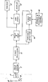
- the senor is a solid state CCD 5 employing a frame transfer type of readout.
- the CCD includes an integration region, a storage region and an output register. Signals generated by an image focussed on the integration region are integrated for a period equivalent to one television field, then transferred rapidly into the opaque storage region during what would be the field flyback period in a standard T.V. system. The output signal is then read out line by line from the storage region via the output register which is of a parallel in, serial out type.
- the serial output is processed by a video processing circuit 10 to produce a video signal.
- the video signal is supplied to a track and hold circuit 11, for a purpose to be described later, and the output from the track and hold circuit is supplied directly to an image tracker device 12 and also, after the addition at 8 of the various synchronisation signals necessary, to a display unit 13.
- the arrangement includes one or more threshold detectors 14 which, during a setting routine, sample the video signal and output a signal indicative of whether the video signal is within the expected limit or limits.
- the output from the threshold detector is stored in a Random Access Memory (RAM) 15 which is addressed in accordance with the location of the particular pixel being sampled by an address and readwrite control unit. That is to say that the address and read and write control unit continually addresses the memory locations of the RAM in synchronism with the pixel output rate of the CCO sensor.
- RAM Random Access Memory
- a suitable form of RAM is a serial video RAM, NEC ⁇ PD41221C, which has an array of 320 vertical X 700 horizontal (total 224000) bits and an access time of 75 ns.
- the sensor includes a lens 17 and a lens cover 18 together with a light source 19 located within the end cap and adapted to provide a diffuse, uniform illumination of the CCD sensor to, for example 50% saturation.
- a setting routine is automatically implemented wherein the CCD sensor is illuminated uniformly by the light source 19 so that blemishes are revealed on the output signal, which is passed to the threshold detector.
- the blemishes typically give a false "peak white” or a dark output and the threshold detector is set so as to ouptut "1"s when the video signal contains peak white or dark outputs and "0"s when it contains the expected output.
- the address and read/write control writes into the appropriate memory location of the RAM either a "0" or a "1” depending on whether the pixel on the sensor to which the memory location corresponds is operating normally or is defective.
- every pixel of the CCD is allocated a blemish location in the RAM, and after the setting routine the RAM contains details of the X,Y co-ordinates of each blemish noted on the sensor.
- the arrangement may switch over to normal operation.
- the threshold detectors are inoperative, and as the video signal for each frame of the CCD is read out, the address and read/write control 16 causes the information concerning each pixel to be read out from the RAM 15 and supplied to the track and hold circuit 11 in synchronism with the corresponding data in the video signal.
- the track and hold circuit 11 tracks the video signal and whilst supplied with "0"s from the video RAM passes the signal unmodified. When however a "1" is supplied to the track and hold circuit, this means that the video signal for that particular pixel is defective.
- the track and hold circuit therefore operates to continue to output the last (non-defective) signal until the track and hold circuit again receives an "0" signal address.
- the arrangement specified above employs a light source to illuminate the sensor during testing. This however is not essential since the testing may be done merely with the lens cap in place, monitoring the dark current of the pixels.
- the system may be used in conjunction with sensors other than CCDs in which blemishes on the sensor have a fixed relationship during use of the sensor.
Landscapes
- Engineering & Computer Science (AREA)
- Multimedia (AREA)
- Signal Processing (AREA)
- Image Input (AREA)
- Transforming Light Signals Into Electric Signals (AREA)
Applications Claiming Priority (2)
| Application Number | Priority Date | Filing Date | Title |
|---|---|---|---|
| GB8526853 | 1985-10-31 | ||
| GB8526853 | 1985-10-31 |
Publications (2)
| Publication Number | Publication Date |
|---|---|
| EP0222548A2 true EP0222548A2 (de) | 1987-05-20 |
| EP0222548A3 EP0222548A3 (de) | 1987-07-29 |
Family
ID=10587536
Family Applications (1)
| Application Number | Title | Priority Date | Filing Date |
|---|---|---|---|
| EP86308361A Withdrawn EP0222548A3 (de) | 1985-10-31 | 1986-10-27 | Bildwandler |
Country Status (1)
| Country | Link |
|---|---|
| EP (1) | EP0222548A3 (de) |
Cited By (7)
| Publication number | Priority date | Publication date | Assignee | Title |
|---|---|---|---|---|
| EP0341700A3 (de) * | 1988-05-10 | 1991-01-02 | Fuji Photo Film Co., Ltd. | Bildeingangsapparat |
| EP0440563A3 (en) * | 1990-01-31 | 1992-04-08 | Sony Corporation | An image defect correcting circuit for a solid state imager |
| EP0615380A1 (de) * | 1993-03-09 | 1994-09-14 | Hughes Aircraft Company | Korrektur von Veränderung in der Ladungsübertragungseffizienz eines ladungsgekoppelten Bildaufnehmers |
| WO1999055081A1 (en) * | 1998-04-17 | 1999-10-28 | Intel Corporation | Calibration of digital cameras |
| EP1418751A1 (de) * | 2002-10-28 | 2004-05-12 | Samsung Electronics Co., Ltd. | CCD-Kamera mit Kompensation defekter Zellen |
| WO2008135095A1 (en) * | 2007-05-04 | 2008-11-13 | Sony Ericsson Mobile Communications Ab | Digital camera device and method for controlling the operation thereof |
| DE102013013022A1 (de) * | 2013-08-06 | 2015-02-12 | Jenoptik Optical Systems Gmbh | Verfahren zur Identifikation defekter Pixel eines Bildaufnahmesensors |
Family Cites Families (2)
| Publication number | Priority date | Publication date | Assignee | Title |
|---|---|---|---|---|
| JPS5373915A (en) * | 1976-12-14 | 1978-06-30 | Sony Corp | Noise eliminating circuit for solid image pickup unit |
| DE3309949A1 (de) * | 1983-03-19 | 1984-09-20 | Agfa-Gevaert Ag, 5090 Leverkusen | Elektronische bildverarbeitungsvorrichtung |
-
1986
- 1986-10-27 EP EP86308361A patent/EP0222548A3/de not_active Withdrawn
Cited By (11)
| Publication number | Priority date | Publication date | Assignee | Title |
|---|---|---|---|---|
| EP0341700A3 (de) * | 1988-05-10 | 1991-01-02 | Fuji Photo Film Co., Ltd. | Bildeingangsapparat |
| EP0440563A3 (en) * | 1990-01-31 | 1992-04-08 | Sony Corporation | An image defect correcting circuit for a solid state imager |
| EP0615380A1 (de) * | 1993-03-09 | 1994-09-14 | Hughes Aircraft Company | Korrektur von Veränderung in der Ladungsübertragungseffizienz eines ladungsgekoppelten Bildaufnehmers |
| WO1999055081A1 (en) * | 1998-04-17 | 1999-10-28 | Intel Corporation | Calibration of digital cameras |
| US6147702A (en) * | 1998-04-17 | 2000-11-14 | Intel Corporation | Calibration of digital cameras |
| GB2351411A (en) * | 1998-04-17 | 2000-12-27 | Intel Corp | Calibration of digital cameras |
| GB2351411B (en) * | 1998-04-17 | 2003-02-12 | Intel Corp | Calibration of digital cameras |
| DE19983110B4 (de) * | 1998-04-17 | 2006-06-29 | Intel Corporation, Santa Clara | Kalibrierung von digitalen Kameras |
| EP1418751A1 (de) * | 2002-10-28 | 2004-05-12 | Samsung Electronics Co., Ltd. | CCD-Kamera mit Kompensation defekter Zellen |
| WO2008135095A1 (en) * | 2007-05-04 | 2008-11-13 | Sony Ericsson Mobile Communications Ab | Digital camera device and method for controlling the operation thereof |
| DE102013013022A1 (de) * | 2013-08-06 | 2015-02-12 | Jenoptik Optical Systems Gmbh | Verfahren zur Identifikation defekter Pixel eines Bildaufnahmesensors |
Also Published As
| Publication number | Publication date |
|---|---|
| EP0222548A3 (de) | 1987-07-29 |
Similar Documents
| Publication | Publication Date | Title |
|---|---|---|
| KR950008708B1 (ko) | 영상 형성 장치 | |
| EP0261917B1 (de) | Änderungsdetektierung in Videodaten | |
| US5140436A (en) | Pre-event/post-event recording in a solid state fast frame recorder | |
| US5195182A (en) | Frame buffer architecture for storing sequential data in alternating memory banks | |
| US5034811A (en) | Video trigger in a solid state motion analysis system | |
| EP0290548A1 (de) | Digitales bilderfassungssystem. | |
| KR100200616B1 (ko) | 감시 화면 분할 표시장치 및 그 방법 | |
| JPH0795821B2 (ja) | 撮像装置 | |
| EP0222548A2 (de) | Bildwandler | |
| EP0130569A2 (de) | Verfahren und Einrichtung zur Bildabtastung | |
| AU2001278180A1 (en) | A method of searching recorded digital video for areas of activity | |
| CA2078374A1 (en) | Method for displaying defect and apparatus therefor | |
| JPH04260275A (ja) | 画像読取装置 | |
| US5742403A (en) | Test apparatus and methods for a digital image scanning system | |
| WO2000074391A1 (en) | Interchangeable ccd camera with integral blemish compensation | |
| US4750210A (en) | Method and apparatus for finding objects within a visual display | |
| KR100394985B1 (ko) | 감시 카메라 | |
| EP0512105B1 (de) | Teleobjektivsensortrigger in einem festkörperkamerabewegungsanalysesystem | |
| JPH1038961A (ja) | 二次元固体撮像デバイスの画素欠陥検出装置 | |
| JP2001171926A (ja) | エレベータかごにおける画像記録方式 | |
| JPS61290880A (ja) | 映像判定装置 | |
| JPH07274178A (ja) | 動きベクトル検出装置 | |
| JPH11160340A (ja) | 監視装置 | |
| JPH0887686A (ja) | 映像監視装置 | |
| JPS61125289A (ja) | 撮像装置 |
Legal Events
| Date | Code | Title | Description |
|---|---|---|---|
| PUAI | Public reference made under article 153(3) epc to a published international application that has entered the european phase |
Free format text: ORIGINAL CODE: 0009012 |
|
| AK | Designated contracting states |
Kind code of ref document: A2 Designated state(s): DE FR GB |
|
| PUAL | Search report despatched |
Free format text: ORIGINAL CODE: 0009013 |
|
| AK | Designated contracting states |
Kind code of ref document: A3 Designated state(s): DE FR GB |
|
| STAA | Information on the status of an ep patent application or granted ep patent |
Free format text: STATUS: THE APPLICATION IS DEEMED TO BE WITHDRAWN |
|
| 18D | Application deemed to be withdrawn |
Effective date: 19880130 |
|
| RIN1 | Information on inventor provided before grant (corrected) |
Inventor name: STEWART, JOHNBRITISH AEROSPACE PUBLIC LTD. COMP. |