EP0222737A2 - Procédé pour la stabilisation d'une membrane pour masque et cadre de support - Google Patents
Procédé pour la stabilisation d'une membrane pour masque et cadre de support Download PDFInfo
- Publication number
- EP0222737A2 EP0222737A2 EP86890315A EP86890315A EP0222737A2 EP 0222737 A2 EP0222737 A2 EP 0222737A2 EP 86890315 A EP86890315 A EP 86890315A EP 86890315 A EP86890315 A EP 86890315A EP 0222737 A2 EP0222737 A2 EP 0222737A2
- Authority
- EP
- European Patent Office
- Prior art keywords
- mask film
- mask
- temperature
- frame
- film
- Prior art date
- Legal status (The legal status is an assumption and is not a legal conclusion. Google has not performed a legal analysis and makes no representation as to the accuracy of the status listed.)
- Granted
Links
Images
Classifications
-
- G—PHYSICS
- G03—PHOTOGRAPHY; CINEMATOGRAPHY; ANALOGOUS TECHNIQUES USING WAVES OTHER THAN OPTICAL WAVES; ELECTROGRAPHY; HOLOGRAPHY
- G03F—PHOTOMECHANICAL PRODUCTION OF TEXTURED OR PATTERNED SURFACES, e.g. FOR PRINTING, FOR PROCESSING OF SEMICONDUCTOR DEVICES; MATERIALS THEREFOR; ORIGINALS THEREFOR; APPARATUS SPECIALLY ADAPTED THEREFOR
- G03F1/00—Originals for photomechanical production of textured or patterned surfaces, e.g., masks, photo-masks, reticles; Mask blanks or pellicles therefor; Containers specially adapted therefor; Preparation thereof
- G03F1/22—Masks or mask blanks for imaging by radiation of 100nm or shorter wavelength, e.g. X-ray masks, extreme ultraviolet [EUV] masks; Preparation thereof
-
- G—PHYSICS
- G03—PHOTOGRAPHY; CINEMATOGRAPHY; ANALOGOUS TECHNIQUES USING WAVES OTHER THAN OPTICAL WAVES; ELECTROGRAPHY; HOLOGRAPHY
- G03F—PHOTOMECHANICAL PRODUCTION OF TEXTURED OR PATTERNED SURFACES, e.g. FOR PRINTING, FOR PROCESSING OF SEMICONDUCTOR DEVICES; MATERIALS THEREFOR; ORIGINALS THEREFOR; APPARATUS SPECIALLY ADAPTED THEREFOR
- G03F7/00—Photomechanical, e.g. photolithographic, production of textured or patterned surfaces, e.g. printing surfaces; Materials therefor, e.g. comprising photoresists; Apparatus specially adapted therefor
- G03F7/20—Exposure; Apparatus therefor
- G03F7/2002—Exposure; Apparatus therefor with visible light or UV light, through an original having an opaque pattern on a transparent support, e.g. film printing, projection printing; by reflection of visible or UV light from an original such as a printed image
-
- G—PHYSICS
- G03—PHOTOGRAPHY; CINEMATOGRAPHY; ANALOGOUS TECHNIQUES USING WAVES OTHER THAN OPTICAL WAVES; ELECTROGRAPHY; HOLOGRAPHY
- G03F—PHOTOMECHANICAL PRODUCTION OF TEXTURED OR PATTERNED SURFACES, e.g. FOR PRINTING, FOR PROCESSING OF SEMICONDUCTOR DEVICES; MATERIALS THEREFOR; ORIGINALS THEREFOR; APPARATUS SPECIALLY ADAPTED THEREFOR
- G03F7/00—Photomechanical, e.g. photolithographic, production of textured or patterned surfaces, e.g. printing surfaces; Materials therefor, e.g. comprising photoresists; Apparatus specially adapted therefor
- G03F7/70—Microphotolithographic exposure; Apparatus therefor
- G03F7/70691—Handling of masks or workpieces
- G03F7/707—Chucks, e.g. chucking or un-chucking operations or structural details
-
- G—PHYSICS
- G03—PHOTOGRAPHY; CINEMATOGRAPHY; ANALOGOUS TECHNIQUES USING WAVES OTHER THAN OPTICAL WAVES; ELECTROGRAPHY; HOLOGRAPHY
- G03F—PHOTOMECHANICAL PRODUCTION OF TEXTURED OR PATTERNED SURFACES, e.g. FOR PRINTING, FOR PROCESSING OF SEMICONDUCTOR DEVICES; MATERIALS THEREFOR; ORIGINALS THEREFOR; APPARATUS SPECIALLY ADAPTED THEREFOR
- G03F7/00—Photomechanical, e.g. photolithographic, production of textured or patterned surfaces, e.g. printing surfaces; Materials therefor, e.g. comprising photoresists; Apparatus specially adapted therefor
- G03F7/70—Microphotolithographic exposure; Apparatus therefor
- G03F7/708—Construction of apparatus, e.g. environment aspects, hygiene aspects or materials
- G03F7/70858—Environment aspects, e.g. pressure of beam-path gas, temperature
- G03F7/70866—Environment aspects, e.g. pressure of beam-path gas, temperature of mask or workpiece
-
- G—PHYSICS
- G03—PHOTOGRAPHY; CINEMATOGRAPHY; ANALOGOUS TECHNIQUES USING WAVES OTHER THAN OPTICAL WAVES; ELECTROGRAPHY; HOLOGRAPHY
- G03F—PHOTOMECHANICAL PRODUCTION OF TEXTURED OR PATTERNED SURFACES, e.g. FOR PRINTING, FOR PROCESSING OF SEMICONDUCTOR DEVICES; MATERIALS THEREFOR; ORIGINALS THEREFOR; APPARATUS SPECIALLY ADAPTED THEREFOR
- G03F7/00—Photomechanical, e.g. photolithographic, production of textured or patterned surfaces, e.g. printing surfaces; Materials therefor, e.g. comprising photoresists; Apparatus specially adapted therefor
- G03F7/70—Microphotolithographic exposure; Apparatus therefor
- G03F7/708—Construction of apparatus, e.g. environment aspects, hygiene aspects or materials
- G03F7/70858—Environment aspects, e.g. pressure of beam-path gas, temperature
- G03F7/70866—Environment aspects, e.g. pressure of beam-path gas, temperature of mask or workpiece
- G03F7/70875—Temperature, e.g. temperature control of masks or workpieces via control of stage temperature
Definitions
- the invention relates to a method for stabilizing masks consisting of a masking film and a holding frame for this film, which masks during operation of a thermal stress through an imaging medium, for. B. ions, electrons or X-rays, are exposed, in the mask film for the imaging medium permeable areas are present.
- the mask film is connected to a preferably metallic mask frame at a suitable temperature. If the thermal expansion coefficient of the mask frame is lower than that of the mask film, then the mask film is anchored in the frame at elevated temperature, for example an nickel mask mask is anchored in an INVAR frame at 60 °, according to a proposal not belonging to the prior art. In the opposite case, clamping, for example a nickel mask foil in an aluminum frame, takes place at a low temperature, for example at -20 ° C. After cooling to room temperature or after warming up to room temperature, the mask film is pretensioned in the frame.
- the object of the invention is to enable masks to be stabilized under a considerably higher load by the imaging medium than is hitherto possible with thermally prestressed masks and at the same time to avoid distortions of intolerable dimensions, even when masks with structure openings are used. This is achieved if, according to the invention, masks, the mask film of which are arranged in the holder free of tension or with such a low pre-tension that distortions of structures in or on the mask film associated with the pre-tension are negligible, in a one located in the imaging device Clamping frames are clamped and the frame is heated to a temperature during operation of the imaging device, which exceeds the temperature that the masking film assumes during operation.
- the mask film can g srahmen doing about the manufacturing process with a anchorages 2 be connected. Technological methods ensure that the mask film has only a low tension, and that the associated distortions of structures in or on the mask film are negligible for the transfer process. For manufacturing reasons, silicon or glass are the most suitable materials for the anchoring frame 2.
- the method according to the invention has the effect that, via the clamping frame, which is in contact with the holder of the mask film, the holder of the mask film is heated in a controlled manner and thus the mask film heated by the imaging medium, which can assume the respective size unhindered by the heating. In this way, a completely stress-free mask can be realized even under high stress from the imaging medium.
- the prestressing of the mask film is preferably kept in the range corresponding to an elongation of 10 -5 to 10, so that only slight distortions, which are negligible, can be expected when the structures of the mask are transferred.
- the holder is typically heated 10 times higher than is necessary to keep the mask film straight. In this way, a very low tension is generated in the mask film, so that on the one hand mechanical vibrations cannot be transmitted to the stress-free mask and on the other hand fluctuations in the loading of the mask film by the imaging medium can be permitted.
- the mask film is brought to a temperature which is at least equal to the temperature of the by supplying a heating medium Mask film at the time of the failure of the imaging medium.
- the heating medium can be emitted from an infrared source or another corpuscular radiation source. If the mask film sags under the heating effect, this is irrelevant for the further use of the film, since after a temperature reduction, the film tightens again.
- the measurement of Maskentem perature can be done in pyrometric way. If the temperature drops, the additional heat source is switched on. It can be the additional source even in continuous operation work, but with reduced intensity, the intensity then being increased accordingly if the imaging medium fails.
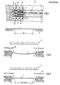
- 1 denotes a masking film, which has a frame 2, for. B. of silicon is anchored.
- the thickness of the mask film 1 is 1 to 5 ⁇ m.
- the mask film 1 is preferably held together with the anchoring frame 2 in a holding frame, which consists of an upper frame 3 and a lower frame 4, to form a mask.
- highly thermally conductive elastic layers 8, 9, for. B. can be arranged from an elastomer.
- the mask film 1 is held in the holding frame 3, 4 tension-free or with only a slight pretension.
- Upper frame 3 and lower frame 4 can be connected to each other by screws 5.
- the holder for the mask film 1 is formed by the anchoring frame 2 and the holding frame, consisting of the upper frame 3 and the lower frame 4.
- the bracket can also be formed only by the anchoring frame 2.
- the holding frame makes handling the mask easier.
- the mask film 1 can be biased so that its stretching is between 10 -5 and 10 -6 .
- ⁇ l denotes the change in length compared to the initial length l o
- the Output length 1 0 corresponds to the length at a reference temperature, eg room temperature.
- the holding frame 3, 4 made of a good heat-conducting material is held in the imaging device between disk-like jaws 6, 7 of a clamping frame.
- a good heat-conducting elastic layer 8, 9, for example made of an elastomer, can also be arranged between the jaws 6, 7 and the holding frame 3, 4.
- the jaws 6, 7 made of a good heat-conducting material can be provided with channels 10 through which a heating medium - if required also a cooling medium - can be passed. Heating wires could also be provided in the jaws 6, 7 of the clamping frame, if necessary in addition to the channels 10.
- the mask film 1 and the holding frame 3, 4 preferably have approximately the same expansion coefficient.
- the frame 3, 4 or the clamping jaws 6, 7 are heated to a temperature exceeding the temperature of the mask film 1, e.g. B. by passing a suitably heated heat transfer medium through the channels 10 of the jaws 6, 7 or by connecting the heating wires built into the jaws 6, 7 to an electrical power supply.
- Operating temperatures of 100 - 200 ° C are common in an ion projector. If one assumes a working temperature of 100 ° C., the frame 3, 4 or the clamping jaws 6, 7 are heated to a temperature of, for example, 110 °. In the case of an INVAR frame that holds a masking film with a diameter of 50 mm, this means, for example, an enlargement of 0.5 ⁇ m.
- FIG. 2 In the upper part of FIG. 2 there is a mask the mask film 1 and the anchoring frame 2 shown. A distance s is drawn on the mask foil. If the mask is now heated by an ion current 11 which - due to the arrangement of the aperture 12 - only hits the mask film 1, the mask expands and sags. This leads to distortions in the image. To switch this off, the frame 3, 4 is heated above the temperature of the mask film 1, as a result of which the film 1 is stretched. The distance s has been extended by ⁇ s. This extension can be optically corrected - if at all necessary - by changing the image ratio. Distortions, such as occur when the mask film sag, are excluded, since the mask film 1 is flat.
Landscapes
- Physics & Mathematics (AREA)
- General Physics & Mathematics (AREA)
- Health & Medical Sciences (AREA)
- Life Sciences & Earth Sciences (AREA)
- Atmospheric Sciences (AREA)
- Toxicology (AREA)
- Engineering & Computer Science (AREA)
- Environmental & Geological Engineering (AREA)
- Epidemiology (AREA)
- Public Health (AREA)
- Preparing Plates And Mask In Photomechanical Process (AREA)
- Exposure And Positioning Against Photoresist Photosensitive Materials (AREA)
- Exposure Of Semiconductors, Excluding Electron Or Ion Beam Exposure (AREA)
- Electron Beam Exposure (AREA)
- Processes Of Treating Macromolecular Substances (AREA)
- Crystals, And After-Treatments Of Crystals (AREA)
- Magnetic Heads (AREA)
Applications Claiming Priority (2)
| Application Number | Priority Date | Filing Date | Title |
|---|---|---|---|
| AT0331185A ATA331185A (de) | 1985-11-13 | 1985-11-13 | Verfahren zum stabilisieren von masken |
| AT3311/85 | 1985-11-13 |
Publications (3)
| Publication Number | Publication Date |
|---|---|
| EP0222737A2 true EP0222737A2 (fr) | 1987-05-20 |
| EP0222737A3 EP0222737A3 (en) | 1989-06-28 |
| EP0222737B1 EP0222737B1 (fr) | 1994-10-12 |
Family
ID=3548590
Family Applications (1)
| Application Number | Title | Priority Date | Filing Date |
|---|---|---|---|
| EP86890315A Expired - Lifetime EP0222737B1 (fr) | 1985-11-13 | 1986-11-13 | Procédé pour la stabilisation d'une membrane pour masque et cadre de support |
Country Status (5)
| Country | Link |
|---|---|
| US (1) | US4775797A (fr) |
| EP (1) | EP0222737B1 (fr) |
| JP (1) | JPH0766181B2 (fr) |
| AT (2) | ATA331185A (fr) |
| DE (1) | DE3650093D1 (fr) |
Cited By (3)
| Publication number | Priority date | Publication date | Assignee | Title |
|---|---|---|---|---|
| AT393334B (de) * | 1988-01-22 | 1991-09-25 | Ims Ionen Mikrofab Syst | Anordnung zur stabilisierung einer bestrahlten maske |
| EP0690347A1 (fr) * | 1994-06-30 | 1996-01-03 | Motorola, Inc. | Méthode lithographique par rayons X pour irradier un objet afin de réaliser un motif sur cet objet |
| WO2015007557A1 (fr) * | 2013-07-16 | 2015-01-22 | Carl Zeiss Smt Gmbh | Composant optique |
Families Citing this family (5)
| Publication number | Priority date | Publication date | Assignee | Title |
|---|---|---|---|---|
| GB2230784B (en) * | 1989-03-21 | 1992-11-18 | Ciba Geigy Ag | Process for modifying acrylate copolymers |
| JP3168952B2 (ja) * | 1997-09-03 | 2001-05-21 | 日本電気株式会社 | 電子ビーム描画用アパーチャ装置とその製造方法 |
| US7786607B2 (en) | 2004-02-19 | 2010-08-31 | Asml Holding N.V. | Overlay correction by reducing wafer slipping after alignment |
| DE602005012945D1 (de) * | 2005-07-20 | 2009-04-09 | Zeiss Carl Sms Gmbh | Teilchenstrahlbelichtungssystem und Vorrichtung zur Strahlbeeinflussung |
| CN105383151A (zh) * | 2015-12-01 | 2016-03-09 | 深圳市和誉达科技有限公司 | 一种网版的制作工艺 |
Family Cites Families (5)
| Publication number | Priority date | Publication date | Assignee | Title |
|---|---|---|---|---|
| DE2606169C2 (de) * | 1976-02-17 | 1983-09-01 | Polymer-Physik GmbH & Co KG, 2844 Lemförde | Elektronenaustrittsfenster für eine Elektronenstrahlquelle |
| AT371947B (de) * | 1979-12-27 | 1983-08-10 | Rudolf Sacher Ges M B H | Freitragende maske, verfahren zur herstellung derselben und verfahren zum maskieren von substraten |
| US4307556A (en) * | 1980-04-01 | 1981-12-29 | Laurel Bank Machine Co., Ltd. | Coin irregularity process machine for coin packaging machine |
| JPS57169244A (en) * | 1981-04-13 | 1982-10-18 | Canon Inc | Temperature controller for mask and wafer |
| AT383438B (de) * | 1981-12-04 | 1987-07-10 | Rudolf Sacher Ges M B H | Freitragende maske |
-
1985
- 1985-11-13 AT AT0331185A patent/ATA331185A/de not_active Application Discontinuation
-
1986
- 1986-11-13 JP JP27082286A patent/JPH0766181B2/ja not_active Expired - Lifetime
- 1986-11-13 DE DE3650093T patent/DE3650093D1/de not_active Expired - Fee Related
- 1986-11-13 AT AT86890315T patent/ATE112867T1/de not_active IP Right Cessation
- 1986-11-13 US US06/930,805 patent/US4775797A/en not_active Expired - Fee Related
- 1986-11-13 EP EP86890315A patent/EP0222737B1/fr not_active Expired - Lifetime
Cited By (6)
| Publication number | Priority date | Publication date | Assignee | Title |
|---|---|---|---|---|
| AT393334B (de) * | 1988-01-22 | 1991-09-25 | Ims Ionen Mikrofab Syst | Anordnung zur stabilisierung einer bestrahlten maske |
| EP0325575B1 (fr) * | 1988-01-22 | 1994-09-07 | IMS Ionen Mikrofabrikations Systeme Gesellschaft m.b.H. | Dispositif de stabilisation d'un masque illuminé |
| EP0690347A1 (fr) * | 1994-06-30 | 1996-01-03 | Motorola, Inc. | Méthode lithographique par rayons X pour irradier un objet afin de réaliser un motif sur cet objet |
| WO2015007557A1 (fr) * | 2013-07-16 | 2015-01-22 | Carl Zeiss Smt Gmbh | Composant optique |
| CN105474100A (zh) * | 2013-07-16 | 2016-04-06 | 卡尔蔡司Smt有限责任公司 | 光学部件 |
| US9915872B2 (en) | 2013-07-16 | 2018-03-13 | Carl Zeiss Smt Gmbh | Optical component |
Also Published As
| Publication number | Publication date |
|---|---|
| DE3650093D1 (de) | 1994-11-17 |
| US4775797A (en) | 1988-10-04 |
| ATA331185A (de) | 1994-05-15 |
| JPH0766181B2 (ja) | 1995-07-19 |
| JPS62118351A (ja) | 1987-05-29 |
| EP0222737A3 (en) | 1989-06-28 |
| ATE112867T1 (de) | 1994-10-15 |
| EP0222737B1 (fr) | 1994-10-12 |
Similar Documents
| Publication | Publication Date | Title |
|---|---|---|
| DE2819698C2 (de) | Verfahren zum Herstellen eines Festkörpermikrobauelementes und Vorrichtung zur Anwendung bei diesem Verfahren | |
| DE69229432T2 (de) | Probenhalter für Elektronenmikroskop | |
| DE69232896T2 (de) | Verfahren für anodische Bindung mit Lichtstrahlung | |
| DE69819971T2 (de) | Vorbehandelte Kristalle aus Lithiumniobat und Lithiumtantalat und das Verfahren zu ihrer Herstellung | |
| DE2924920A1 (de) | Verfahren zur herstellung grobkristalliner oder einkristalliner metalloder legierungsschichten | |
| DE102015107819B4 (de) | Niedrigtemperatur-Abdeckglasfritte und Verfahren zur Herstellung eines Verbund-Füllstoffs in einer Glasfritte | |
| DE3137441A1 (de) | Verfahren zum befestigen von optischen und elektrooptischen bauelementen | |
| EP0435999B1 (fr) | Capteur de temperature et son procede de production | |
| EP0222737A2 (fr) | Procédé pour la stabilisation d'une membrane pour masque et cadre de support | |
| DE1302005C2 (de) | Verwendung eines metallischen ueberzugs als grossflaechiger anschluss fuer plenare halbleiterbauelemente | |
| DE102020207099A1 (de) | Verfahren und Vorrichtung zur Herstellung eines optischen Elementes | |
| DE2558752C3 (de) | Verfahren zur Herstellung eines Schichrwiderstandes als Meßwiderstand für Widerstandsthermometer | |
| DE2638114A1 (de) | Verfahren zum fuellen von oeffnungen mit kristallinem werkstoff | |
| DE2832117A1 (de) | Gasentladungslaservorrichtung | |
| DE102020000902A1 (de) | Vorrichtung zum Produzieren von polykristallinem Silicium und polykristallines Silicium | |
| EP0785870B1 (fr) | Procede de modification de la courbure de corps composites plats anodiquement lies en verre et metal ou materiaux semi-conducteurs | |
| DE2900747A1 (de) | Verfahren zur herstellung einer halbleiteranordnung | |
| DE3784138T2 (de) | Quarz-quadrupol fuer massenfilter. | |
| DE4410315A1 (de) | Mikrosensor zur Messung der spezifischen Wärmeleitfähigkeit dünner Schichten | |
| EP0223770B1 (fr) | Dispositif pour éviter des déformations plastiques d'une feuille de masquage | |
| DE2621418C2 (de) | Verfahren und Vorrichtung zum Dotieren von Halbleiterplättchen | |
| DE2025376C3 (de) | Einkristall-Züchtungsverfahren für Bariumnatriumniobat und verwandte Verbindungen | |
| DE102021004175B3 (de) | Abstandsvorrichtung für Heizsystem zum Aufheizen von großflächigen Substraten, Heizsystem und Aufheizverfahren | |
| DE3718197A1 (de) | Verfahren zur herstellung eines thermistors mit negativem temperaturkoeffizienten | |
| EP0056972A1 (fr) | Procédé et installation pour la fabrication des éléments semiconducteurs selon des paramètres physiques déterminés |
Legal Events
| Date | Code | Title | Description |
|---|---|---|---|
| PUAI | Public reference made under article 153(3) epc to a published international application that has entered the european phase |
Free format text: ORIGINAL CODE: 0009012 |
|
| AK | Designated contracting states |
Kind code of ref document: A2 Designated state(s): AT BE DE FR GB IT NL SE |
|
| PUAL | Search report despatched |
Free format text: ORIGINAL CODE: 0009013 |
|
| AK | Designated contracting states |
Kind code of ref document: A3 Designated state(s): AT BE DE FR GB IT NL SE |
|
| 17P | Request for examination filed |
Effective date: 19891212 |
|
| RAP1 | Party data changed (applicant data changed or rights of an application transferred) |
Owner name: IMS IONEN MIKROFABRIKATIONS SYSTEME GESELLSCHAFT M Owner name: OESTERREICHISCHE INVESTITIONSKREDIT AKTIENGESELLS |
|
| 17Q | First examination report despatched |
Effective date: 19911021 |
|
| GRAA | (expected) grant |
Free format text: ORIGINAL CODE: 0009210 |
|
| AK | Designated contracting states |
Kind code of ref document: B1 Designated state(s): AT BE DE FR GB IT NL SE |
|
| PG25 | Lapsed in a contracting state [announced via postgrant information from national office to epo] |
Ref country code: IT Free format text: LAPSE BECAUSE OF FAILURE TO SUBMIT A TRANSLATION OF THE DESCRIPTION OR TO PAY THE FEE WITHIN THE PRE;WARNING: LAPSES OF ITALIAN PATENTS WITH EFFECTIVE DATE BEFORE 2007 MAY HAVE OCCURRED AT ANY TIME BEFORE 2007. THE CORRECT EFFECTIVE DATE MAY BE DIFFERENT FROM THE ONE RECORDED.SCRIBED TIME-LIMIT Effective date: 19941012 Ref country code: NL Effective date: 19941012 Ref country code: BE Effective date: 19941012 |
|
| PGFP | Annual fee paid to national office [announced via postgrant information from national office to epo] |
Ref country code: FR Payment date: 19941012 Year of fee payment: 9 |
|
| REF | Corresponds to: |
Ref document number: 112867 Country of ref document: AT Date of ref document: 19941015 Kind code of ref document: T |
|
| PGFP | Annual fee paid to national office [announced via postgrant information from national office to epo] |
Ref country code: GB Payment date: 19941013 Year of fee payment: 9 |
|
| PGFP | Annual fee paid to national office [announced via postgrant information from national office to epo] |
Ref country code: DE Payment date: 19941014 Year of fee payment: 9 |
|
| PG25 | Lapsed in a contracting state [announced via postgrant information from national office to epo] |
Ref country code: AT Effective date: 19941113 |
|
| REF | Corresponds to: |
Ref document number: 3650093 Country of ref document: DE Date of ref document: 19941117 |
|
| GBT | Gb: translation of ep patent filed (gb section 77(6)(a)/1977) |
Effective date: 19941101 |
|
| PG25 | Lapsed in a contracting state [announced via postgrant information from national office to epo] |
Ref country code: SE Effective date: 19950112 |
|
| ET | Fr: translation filed | ||
| NLV1 | Nl: lapsed or annulled due to failure to fulfill the requirements of art. 29p and 29m of the patents act | ||
| PLBE | No opposition filed within time limit |
Free format text: ORIGINAL CODE: 0009261 |
|
| STAA | Information on the status of an ep patent application or granted ep patent |
Free format text: STATUS: NO OPPOSITION FILED WITHIN TIME LIMIT |
|
| 26N | No opposition filed | ||
| PG25 | Lapsed in a contracting state [announced via postgrant information from national office to epo] |
Ref country code: GB Effective date: 19951113 |
|
| GBPC | Gb: european patent ceased through non-payment of renewal fee |
Effective date: 19951113 |
|
| PG25 | Lapsed in a contracting state [announced via postgrant information from national office to epo] |
Ref country code: FR Effective date: 19960731 |
|
| PG25 | Lapsed in a contracting state [announced via postgrant information from national office to epo] |
Ref country code: DE Effective date: 19960801 |
|
| REG | Reference to a national code |
Ref country code: FR Ref legal event code: ST |