EP0222943B1 - Codeur à mots à longueur variable - Google Patents
Codeur à mots à longueur variable Download PDFInfo
- Publication number
- EP0222943B1 EP0222943B1 EP85308006A EP85308006A EP0222943B1 EP 0222943 B1 EP0222943 B1 EP 0222943B1 EP 85308006 A EP85308006 A EP 85308006A EP 85308006 A EP85308006 A EP 85308006A EP 0222943 B1 EP0222943 B1 EP 0222943B1
- Authority
- EP
- European Patent Office
- Prior art keywords
- signal
- magnitude
- bit
- binary word
- word
- Prior art date
- Legal status (The legal status is an assumption and is not a legal conclusion. Google has not performed a legal analysis and makes no representation as to the accuracy of the status listed.)
- Expired
Links
- 230000003111 delayed effect Effects 0.000 claims description 12
- 230000001419 dependent effect Effects 0.000 claims 1
- 230000005540 biological transmission Effects 0.000 description 2
- 230000003044 adaptive effect Effects 0.000 description 1
- 238000006243 chemical reaction Methods 0.000 description 1
- 238000000034 method Methods 0.000 description 1
Images
Classifications
-
- H—ELECTRICITY
- H03—ELECTRONIC CIRCUITRY
- H03M—CODING; DECODING; CODE CONVERSION IN GENERAL
- H03M5/00—Conversion of the form of the representation of individual digits
- H03M5/02—Conversion to or from representation by pulses
- H03M5/04—Conversion to or from representation by pulses the pulses having two levels
- H03M5/14—Code representation, e.g. transition, for a given bit cell depending on the information in one or more adjacent bit cells, e.g. delay modulation code, double density code
- H03M5/145—Conversion to or from block codes or representations thereof
-
- H—ELECTRICITY
- H03—ELECTRONIC CIRCUITRY
- H03M—CODING; DECODING; CODE CONVERSION IN GENERAL
- H03M7/00—Conversion of a code where information is represented by a given sequence or number of digits to a code where the same, similar or subset of information is represented by a different sequence or number of digits
- H03M7/30—Compression; Expansion; Suppression of unnecessary data, e.g. redundancy reduction
- H03M7/40—Conversion to or from variable length codes, e.g. Shannon-Fano code, Huffman code, Morse code
- H03M7/42—Conversion to or from variable length codes, e.g. Shannon-Fano code, Huffman code, Morse code using table look-up for the coding or decoding process, e.g. using read-only memory
-
- H—ELECTRICITY
- H04—ELECTRIC COMMUNICATION TECHNIQUE
- H04J—MULTIPLEX COMMUNICATION
- H04J3/00—Time-division multiplex systems
- H04J3/16—Time-division multiplex systems in which the time allocation to individual channels within a transmission cycle is variable, e.g. to accommodate varying complexity of signals, to vary number of channels transmitted
- H04J3/1682—Allocation of channels according to the instantaneous demands of the users, e.g. concentrated multiplexers, statistical multiplexers
- H04J3/1688—Allocation of channels according to the instantaneous demands of the users, e.g. concentrated multiplexers, statistical multiplexers the demands of the users being taken into account after redundancy removal, e.g. by predictive coding, by variable sampling
Definitions
- the invention relates to variable word length coders for digital signals and is especially, but not exclusively, applicable to predictive differential pulse code modulation systems for video or voice transmission and/or storage.
- variable word length coder which has shorter words assigned to the inner levels around zero, where the probability of data generation is high.
- One known possibility is to apply the output of the coder, in parallel form, to a parallel to serial converter and thence to a serial buffer memory.
- the buffer memory must have a capacity and writing rate sufficient to accommodate the longest variable word length coded word at the basic system frequency. For example, if a clock frequency is 8 MHZ and the longest word is 25 bits long, then the rate of writing the data into the buffer memory varies between 8 megabits per second and 200 megabits per second. Accordingly, hardware to handle such a speed is difficult zu realize.
- difficulty arises in parallel to serial conversion when the size of the words at the input to the parallel to serial converter is inherently variable.
- An object of the present invention is to eliminate or at least mitigate these disadvantages.
- apparatus for variable word-length encoding of input signals comprising fixed length binary words comprises:
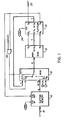
- Figure 1 is a schematic representation of a variable word length encoder deriving its input from a parallel buffer memory.
- an encoder for encoding binary words of fixed length into words of variable length comprises selection means in the form of a multiplexer (MUX) 10, having two input sets, denoted A and B, each of eight inputs; memory means in the form of a read-only memory (ROM) 12; and output delay means in the form of a flip-flop 14.
- MUX multiplexer
- ROM read-only memory
- output delay means in the form of a flip-flop 14.
- Six bit parallel signed binary words are supplied to the encoder from input storage means in the form-of a parallel buffer remory 16, which has an input bus 18 to receive such words from a suitable source (not shown).
- a typical source is the quantizer output of a predictive encoder as used in an adaptive differential pulse code modulation system.
- Table 1 illustrates, for levels ranging from -13 to +13, the signed binary representation of such a quantizer output.
- Each such binary word has one bit denoting its polarity and five bits representing its magnitude. It will be appreciated that although only thirteen levels are shown in the table, the five bits will give a range of 31 levels, and even greater ranges can be achieved merely by increasing the number of bits.
- the third column of table 1 shows a typical variable length word for each level. It will be noted that the zero level is unique in that its corresponding output word is a single '0' bit. All other variable output words have in common a start bit (1), a polarity bit (1 or 0), end bit (1) and an intervening series of zero bits, the number of which depends upon the numerical level. More specifically, the number of zero bits is one less than the level number. Thus, the variable length words representing level one have no zero magnitude bits (note that the zero in the plus one representation is a polarity bit) and the words representing level thirteen have twelve intervening zero bits. As mentioned in the introduction, the utility of the code is predicted upon the fact that the quantizer output remains close to zero because of the correlation between neighbouring elements of the voice or video signal being encoded. Therefore, on average the output word will be shorter than the corresponding six-bit input word.
- the binary words from the buffer memory 16 are applied by way of a six- line bus to inputs B i to B 6 of the multiplexer 10.
- the remaining two inputs of that set, 8 7 and 8 8 are maintained permanently at binary levels "0" and "1" respectively. This may be done by connecting inputs 8 7 and 8 8 to a low and a high voltage source, respectively. These two bits serve as a first control signal, as will be explained hereafter.
- the corresponding eight-bit words output from the multiplexer 10 are applied to the address inputs of the ROM 12. Each produces a nine-bit output word at outputs Q 0 -Q 8 respectively, of the ROM 12.
- Output Qo is coupled individually via the flip-flop 14 to the serial output terminal 22 of the encoder.
- ROM outputs Q 1 to Q 7 are applied by way of the flip-flop 14 to inputs A 1 to A 7 of the multiplexer 10.
- the most significant bit of the ROM output, Q 8 is coupled individually via the flip-flop 14 to the CLOCK-OUT input of the buffer memory 16, and to inputs A 8 and select (SLCT) of the multiplexer 10.
- the flip-flop 14 which is controlled by a clock 24, serves to delay or store the ROM output during any one bit period for application to the output 22 and multiplexer 10 during the next bit period.
- Levels "1" and “0" at its SLCT input cause the multiplexer 10 to connect input sets "B” and “A”, respectively, to the ROM address.
- Operation of the apparatus may be initiated by means of an OR gate 26 interposed between the flip-flop 14 and the SLCT input of the multiplexer 10, whereby the multiplexer 10 can be made to select inputs B to receive a new binary word.
- the apparatus has two basic modes of operation (i) and (ii) depending upon whether or not the binary word at the multiplexer's B inputs has a magnitude of zero.
- the feedback part of the ROM output, bits Q to Or. will comprise a magnitude part (00000), a sign bit (0), a control bit (0), and the most significant bit, Q 8 , will again be (1) as the multiplexer 10 will maintain selection of the B inputs for application to the ROM address and a new six-bit binary word will be clocked out of the buffer memory 16.
- a second control signal comprising a (0) as the most significant bit (generated by the ROM output in the preceding step) appears at the ROM address. So long as the associated magnitude is greater than unity, the corresponding ROM output will comprise the second control signal comprising a (0) in the most significant bit, a magnitude part having a numerical value of one less than that of the magnitude of the addressing word, and a (0) as the serial output Qo. Accordingly, the apparatus "counts down" the binary input word and in the process generates a series of zeros in the variable length output word.
- the corresponding ROM output comprises the first control signal comprising a (1) in the most significant bit again, a magnitude of zero, and a '1' as the serial output bit. This terminates the series of steps since the most significant bit Q 8 is (1), causing the multiplexer 10 to select inputs B again to input a new binary word from the buffer memory 16.
- the third step is also the last and no string of zeros representing magnitude is generated. It will be noted that for level plus one there is a single zero in the variable length output word. However, this zero represents polarity. The polarity-representing bit always appears as the second bit of the variable length output word and is therefore generated in the second step.
- the ROM output produces a (0) as the most significant bit, Os.
- the ROM produces a (1) as the second most significant bit 0 7 .
- the ROM address comprises a second control signal comprising a (0) in the most significant bit and a third control signal comprising a (1) in the second most significant bit.
- the remainder of the address is the six-bit word, its sign and magnitude bits unchanged, as it was reproduced by the ROM output in the first step.
- the corresponding ROM output in the second step comprises, the second control signal comprising a (0) in the most significant bit, a (0) in the second most significant bit, the magnitude part of the address word, unchanged, and a serial output bit, Qo, which is (1) or (0) depending upon the polarity of the word being encoded.
- the sign bit in the feedback signal can be with or without change because it is irrelevant after the completion of the second step.
- the sign bit Q 6 will be (0) regardless of its value at the input.
- the second step in the series can be omitted.
- the polarity bit might be elsewhere in a non-unity output word, rather than the second bit.
- the additional bit might characterize another feature of the word, for example, the additional bit might merely distinguish between words of similar probability of occurrence. Also, more than one additional bit might be used for these or other purposes.
Landscapes
- Engineering & Computer Science (AREA)
- Theoretical Computer Science (AREA)
- Computer Networks & Wireless Communication (AREA)
- Signal Processing (AREA)
- Compression, Expansion, Code Conversion, And Decoders (AREA)
- Vehicle Body Suspensions (AREA)
- Valve Device For Special Equipments (AREA)
- Valve-Gear Or Valve Arrangements (AREA)
Claims (4)
de sorte que, pour chaque mot binaire d'entrée d'amplitude non nulle, le dispositif produit une sortie comprenant une séquence de bits comportant un premier bit dans le premier état prescrit des deux états possibles suivi par (m-1 ) bits dans l'autre de deux états possibles, suivi par un bit final dans le premier état prescrit de deux états possibles, où m est l'amplitude du premier mot binaire d'entrée.
Priority Applications (5)
| Application Number | Priority Date | Filing Date | Title |
|---|---|---|---|
| CA000440742A CA1207911A (fr) | 1983-11-08 | 1983-11-08 | Codeur de mots de longueur variable |
| US06/551,145 US4568916A (en) | 1983-11-14 | 1983-11-14 | Variable word length encoder |
| EP85308006A EP0222943B1 (fr) | 1983-11-08 | 1985-11-04 | Codeur à mots à longueur variable |
| DE8585308006T DE3576027D1 (de) | 1983-11-08 | 1985-11-04 | Kodierer fuer woerter variabler laenge. |
| AT85308006T ATE50386T1 (de) | 1983-11-08 | 1985-11-04 | Kodierer fuer woerter variabler laenge. |
Applications Claiming Priority (2)
| Application Number | Priority Date | Filing Date | Title |
|---|---|---|---|
| CA000440742A CA1207911A (fr) | 1983-11-08 | 1983-11-08 | Codeur de mots de longueur variable |
| EP85308006A EP0222943B1 (fr) | 1983-11-08 | 1985-11-04 | Codeur à mots à longueur variable |
Publications (2)
| Publication Number | Publication Date |
|---|---|
| EP0222943A1 EP0222943A1 (fr) | 1987-05-27 |
| EP0222943B1 true EP0222943B1 (fr) | 1990-02-07 |
Family
ID=39615624
Family Applications (1)
| Application Number | Title | Priority Date | Filing Date |
|---|---|---|---|
| EP85308006A Expired EP0222943B1 (fr) | 1983-11-08 | 1985-11-04 | Codeur à mots à longueur variable |
Country Status (4)
| Country | Link |
|---|---|
| EP (1) | EP0222943B1 (fr) |
| AT (1) | ATE50386T1 (fr) |
| CA (1) | CA1207911A (fr) |
| DE (1) | DE3576027D1 (fr) |
Family Cites Families (1)
| Publication number | Priority date | Publication date | Assignee | Title |
|---|---|---|---|---|
| US4396906A (en) * | 1980-10-31 | 1983-08-02 | Sri International | Method and apparatus for digital Huffman encoding |
-
1983
- 1983-11-08 CA CA000440742A patent/CA1207911A/fr not_active Expired
-
1985
- 1985-11-04 EP EP85308006A patent/EP0222943B1/fr not_active Expired
- 1985-11-04 DE DE8585308006T patent/DE3576027D1/de not_active Expired - Fee Related
- 1985-11-04 AT AT85308006T patent/ATE50386T1/de not_active IP Right Cessation
Also Published As
| Publication number | Publication date |
|---|---|
| CA1207911A (fr) | 1986-07-15 |
| DE3576027D1 (de) | 1990-03-15 |
| ATE50386T1 (de) | 1990-02-15 |
| EP0222943A1 (fr) | 1987-05-27 |
Similar Documents
| Publication | Publication Date | Title |
|---|---|---|
| US4396906A (en) | Method and apparatus for digital Huffman encoding | |
| US4509038A (en) | Code-converting system for band compression of digital signals | |
| US4568916A (en) | Variable word length encoder | |
| US4237552A (en) | Time division multiplexed transmission systems for telephone or like signals with frequency band compression | |
| US4044347A (en) | Variable-length to fixed-length conversion of minimum-redundancy codes | |
| US3973081A (en) | Feedback residue compression for digital speech systems | |
| US5463699A (en) | Data compression | |
| EP0250049A1 (fr) | Codeur de canal | |
| US4366469A (en) | Companding analog to digital converter | |
| US4580129A (en) | Variable word length decoder | |
| US4503510A (en) | Method and apparatus for digital data compression | |
| US4841299A (en) | Method and apparatus for digital encoding and decoding | |
| US3588364A (en) | Adaptive encoder and decoder | |
| US3772682A (en) | Digital conversion from one pcm format to another | |
| US4037226A (en) | Pulse code modulation compressor | |
| US3646445A (en) | Adaptive extremal coding of analog signals | |
| US4827475A (en) | Transmitting a digital signal and an additional signal | |
| EP0222943A1 (fr) | Codeur à mots à longueur variable | |
| GB1569076A (en) | Digital transmission system using discrepancy line coding | |
| EP0222942A1 (fr) | Décodeur de mots à longueur variable | |
| US4736387A (en) | Quantizing apparatus | |
| US4792794A (en) | Differential pulse code modulation system with neutralization of direct current information | |
| JPS6338898B2 (fr) | ||
| US4534037A (en) | Method and apparatus for scrambled pulse-code modulation transmission or recording | |
| US5016279A (en) | Speech analyzing and synthesizing apparatus using reduced number of codes |
Legal Events
| Date | Code | Title | Description |
|---|---|---|---|
| PUAI | Public reference made under article 153(3) epc to a published international application that has entered the european phase |
Free format text: ORIGINAL CODE: 0009012 |
|
| 17P | Request for examination filed |
Effective date: 19870310 |
|
| AK | Designated contracting states |
Kind code of ref document: A1 Designated state(s): AT DE FR GB NL SE |
|
| 17Q | First examination report despatched |
Effective date: 19880218 |
|
| GRAA | (expected) grant |
Free format text: ORIGINAL CODE: 0009210 |
|
| AK | Designated contracting states |
Kind code of ref document: B1 Designated state(s): AT DE FR GB NL SE |
|
| REF | Corresponds to: |
Ref document number: 50386 Country of ref document: AT Date of ref document: 19900215 Kind code of ref document: T |
|
| REF | Corresponds to: |
Ref document number: 3576027 Country of ref document: DE Date of ref document: 19900315 |
|
| ET | Fr: translation filed | ||
| PG25 | Lapsed in a contracting state [announced via postgrant information from national office to epo] |
Ref country code: GB Effective date: 19901104 Ref country code: AT Effective date: 19901104 |
|
| PG25 | Lapsed in a contracting state [announced via postgrant information from national office to epo] |
Ref country code: SE Effective date: 19901105 |
|
| PLBE | No opposition filed within time limit |
Free format text: ORIGINAL CODE: 0009261 |
|
| STAA | Information on the status of an ep patent application or granted ep patent |
Free format text: STATUS: NO OPPOSITION FILED WITHIN TIME LIMIT |
|
| 26N | No opposition filed | ||
| PG25 | Lapsed in a contracting state [announced via postgrant information from national office to epo] |
Ref country code: NL Effective date: 19910601 |
|
| GBPC | Gb: european patent ceased through non-payment of renewal fee | ||
| NLV4 | Nl: lapsed or anulled due to non-payment of the annual fee | ||
| PG25 | Lapsed in a contracting state [announced via postgrant information from national office to epo] |
Ref country code: FR Effective date: 19910731 |
|
| PG25 | Lapsed in a contracting state [announced via postgrant information from national office to epo] |
Ref country code: DE Effective date: 19910801 |
|
| REG | Reference to a national code |
Ref country code: FR Ref legal event code: ST |
|
| EUG | Se: european patent has lapsed |
Ref document number: 85308006.7 Effective date: 19910705 |