EP0223032A2 - Method for making submicron mask openings using sidewalls and lift-off techniques - Google Patents
Method for making submicron mask openings using sidewalls and lift-off techniques Download PDFInfo
- Publication number
- EP0223032A2 EP0223032A2 EP86113666A EP86113666A EP0223032A2 EP 0223032 A2 EP0223032 A2 EP 0223032A2 EP 86113666 A EP86113666 A EP 86113666A EP 86113666 A EP86113666 A EP 86113666A EP 0223032 A2 EP0223032 A2 EP 0223032A2
- Authority
- EP
- European Patent Office
- Prior art keywords
- film
- substrate
- mesa
- method described
- sidewalls
- Prior art date
- Legal status (The legal status is an assumption and is not a legal conclusion. Google has not performed a legal analysis and makes no representation as to the accuracy of the status listed.)
- Ceased
Links
Images
Classifications
-
- H—ELECTRICITY
- H10—SEMICONDUCTOR DEVICES; ELECTRIC SOLID-STATE DEVICES NOT OTHERWISE PROVIDED FOR
- H10P—GENERIC PROCESSES OR APPARATUS FOR THE MANUFACTURE OR TREATMENT OF DEVICES COVERED BY CLASS H10
- H10P76/00—Manufacture or treatment of masks on semiconductor bodies, e.g. by lithography or photolithography
- H10P76/40—Manufacture or treatment of masks on semiconductor bodies, e.g. by lithography or photolithography of masks comprising inorganic materials
- H10P76/403—Manufacture or treatment of masks on semiconductor bodies, e.g. by lithography or photolithography of masks comprising inorganic materials for lift-off processes
-
- H—ELECTRICITY
- H10—SEMICONDUCTOR DEVICES; ELECTRIC SOLID-STATE DEVICES NOT OTHERWISE PROVIDED FOR
- H10P—GENERIC PROCESSES OR APPARATUS FOR THE MANUFACTURE OR TREATMENT OF DEVICES COVERED BY CLASS H10
- H10P76/00—Manufacture or treatment of masks on semiconductor bodies, e.g. by lithography or photolithography
- H10P76/40—Manufacture or treatment of masks on semiconductor bodies, e.g. by lithography or photolithography of masks comprising inorganic materials
- H10P76/408—Manufacture or treatment of masks on semiconductor bodies, e.g. by lithography or photolithography of masks comprising inorganic materials characterised by their sizes, orientations, dispositions, behaviours or shapes
- H10P76/4085—Manufacture or treatment of masks on semiconductor bodies, e.g. by lithography or photolithography of masks comprising inorganic materials characterised by their sizes, orientations, dispositions, behaviours or shapes characterised by the processes involved to create the masks
-
- Y—GENERAL TAGGING OF NEW TECHNOLOGICAL DEVELOPMENTS; GENERAL TAGGING OF CROSS-SECTIONAL TECHNOLOGIES SPANNING OVER SEVERAL SECTIONS OF THE IPC; TECHNICAL SUBJECTS COVERED BY FORMER USPC CROSS-REFERENCE ART COLLECTIONS [XRACs] AND DIGESTS
- Y10—TECHNICAL SUBJECTS COVERED BY FORMER USPC
- Y10S—TECHNICAL SUBJECTS COVERED BY FORMER USPC CROSS-REFERENCE ART COLLECTIONS [XRACs] AND DIGESTS
- Y10S438/00—Semiconductor device manufacturing: process
- Y10S438/942—Masking
- Y10S438/945—Special, e.g. metal
-
- Y—GENERAL TAGGING OF NEW TECHNOLOGICAL DEVELOPMENTS; GENERAL TAGGING OF CROSS-SECTIONAL TECHNOLOGIES SPANNING OVER SEVERAL SECTIONS OF THE IPC; TECHNICAL SUBJECTS COVERED BY FORMER USPC CROSS-REFERENCE ART COLLECTIONS [XRACs] AND DIGESTS
- Y10—TECHNICAL SUBJECTS COVERED BY FORMER USPC
- Y10S—TECHNICAL SUBJECTS COVERED BY FORMER USPC CROSS-REFERENCE ART COLLECTIONS [XRACs] AND DIGESTS
- Y10S438/00—Semiconductor device manufacturing: process
- Y10S438/942—Masking
- Y10S438/947—Subphotolithographic processing
-
- Y—GENERAL TAGGING OF NEW TECHNOLOGICAL DEVELOPMENTS; GENERAL TAGGING OF CROSS-SECTIONAL TECHNOLOGIES SPANNING OVER SEVERAL SECTIONS OF THE IPC; TECHNICAL SUBJECTS COVERED BY FORMER USPC CROSS-REFERENCE ART COLLECTIONS [XRACs] AND DIGESTS
- Y10—TECHNICAL SUBJECTS COVERED BY FORMER USPC
- Y10S—TECHNICAL SUBJECTS COVERED BY FORMER USPC CROSS-REFERENCE ART COLLECTIONS [XRACs] AND DIGESTS
- Y10S438/00—Semiconductor device manufacturing: process
- Y10S438/942—Masking
- Y10S438/948—Radiation resist
- Y10S438/951—Lift-off
Definitions
- This invention generally relates to methods for making submicron mask openings and more particularly, to such a method characterized by the use of sidewall, reactive-ion etching and image reversal lift-off techniques.
- a new technique has evolved to avoid the inherent optical limitations in the selective exposure of resist materials, as the mask opening size or width of the desired line patterns is reduced to the order of one micron or less for very high density integrated circuits.
- the new technique eliminates the use of photolithography to define the cited dimensions and substitutes a sidewall, reactive-ion etching (RIE) process whereby the dimensions are determined by the thickness of a deposited layer which can be controlled with great accuracy.
- RIE reactive-ion etching
- Submicron mask openings suitable for use with substrates of various types, including non-oxidizable substrates, are produced by a sidewall reactive-ion etching process including image reversal lift-off processing steps.
- a mesa of submicron width is formed on a substrate by sidewall-RIE technique.
- the substrate includes a layer of P+-doped polycrystalline silicon material covered by silicon dioxide and silicon nitride layers.
- the substrate in turn, is formed over an N ⁇ epitaxial silicon layer in which a bipolar transistor is to be made.
- the mesa comprises an underlying layer of silicon dioxide covered by silicon nitride.
- the mesa silicon oxide layer is undercut by isotropic etching to provide a lift-off profile and magnesium oxide (MgO) or other suitable RIE masking material is then deposited over the structure as by evaporation.
- MgO magnesium oxide
- the remaining SiO2 in the mesa support is etched away, lifting off the overlying Si3N4 and MgO layers to leave a submicron opening in the residual MgO film on the non-mesa areas of the structure.
- the substrate exposed through the opening is removed by further RIE to provide an emitter mask for the N ⁇ epitaxial layer of much smaller dimension and with significantly better dimensional control than is achievable using photolithographical methods.
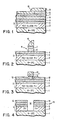
- Figs. 1-4 are simplified, cross-sectional views of the partial structures resulting at successive times during the execution of a preferred embodiment of the method of the present invention.
- the method of the present invention is for the formation of submicron holes in a wide variety of materials, it will be described in the context of materials used in making a submicron emitter mask opening for a polycrystalline base bipolar transistor.
- a transistor of such type is well known in the art and is described, for example, in U.S. Patent No. 4,252,582, issued on February 24, 1981 and assigned to the present assignee. Briefly, the transistor is formed in an epitaxial layer deposited on a monocrystalline semiconductor body. A doped polycrystalline layer (to form at least part of the extrinsic base area by outdiffusion into the epitaxial layer and to provide electrical circuit connection to said extrinsic base) is deposited over the epitaxial layer. Eventually, an emitter is formed centrally within the extrinsic base.
- an exemplary layered mask used in defining an emitter opening in a polycrystalline base transistor comprises P+-doped polycrystalline layer 2, SiO2 layer 3 and Si3N4 layer 4.
- the mask is formed on N epi layer 1 in which the transistor (not shown) is produced.
- Layers 2, 3 and 4 commonly are used in the fabrication of polycrystalline-base transistors but they form no necessary part of the present invention, in its broader aspect, other than to constitute a substrate 5 into which a submicron opening is to be made.
- the width of the desired submicron opening is determined in accordance with the sidewall-reactive ion etching technique of the aforementioned patent 4,209,349 by which the closely controlled thickness of a layer or layers deposited on the surfaces of a stepped structure is reactively ion etched to remove all of the deposited layer except along the vertical surface (sidewall) of the stepped structure. Accordingly, SiO2 layer 6, Si3N4 layer 7 and SiO2 stepped structure 8 are formed on substrate 5. The entire structure is covered by polycrystalline silicon layer 9 and then reactively ion etched to remove the layer 9 from all horizontal surfaces leaving it only at the sidewall 10 of stepped structure 8. The steps carried out to this point generally correspond to those described in patent 4,209,349 although the specific materials employed differ somewhat.
- structure 11 is used in a lift-off process to form a submicron opening in substrate 5 having the dimension and dimensional precision determined by the thickness of deposited layer 9 and without the use of any oxidation step (such as in patent 4,209,349) which would tend to form a "bird's beak" invading the sidewall structure and lessening the precision with which the width of the sidewall structure is maintained. This is achieved by first removing the polycrystalline silicon residue 10.
- the SiO2 layer 6 of structure 11 preferably is undercut by use of a selective etchant and a layer 12 of a suitable lift-off material such as MgO or polysilicon is deposited (as by evaporation) over the structure.
- a layer 12 of a suitable lift-off material such as MgO or polysilicon is deposited (as by evaporation) over the structure.
- the undercut SiO2 and the overlying Si3N4 7 and MgO 12 are removed by use of an isotropic etchant that selectively attacks the SiO2 layer 6 as is well understood in the lift-off processing art.
- the remaining MgO layer 12 then is used as a reactive ion etching mask for the successive removal of the exposed Si3N4, SiO2 and polycrystalline silicon layers 4, 3 and 2, respectively, to yield the structure 13 shown in Fig. 4.
- Structure 13 is compatible with state-of-the-art polycrystalline silicon base transistors where P+ polycrystalline layer 2 of structure 13 provides a base contact to an extrinsic base region (not shown) which is formed by outdiffusion of dopant from layer 2 into epi 1 and the intrinsic base and emitter regions (also not shown) are produced by respective ion implantations through opening 14 in structure 13.
Landscapes
- Bipolar Transistors (AREA)
- Drying Of Semiconductors (AREA)
Abstract
Description
- This invention generally relates to methods for making submicron mask openings and more particularly, to such a method characterized by the use of sidewall, reactive-ion etching and image reversal lift-off techniques.
- Various forms of photolithography have been employed in the making of mask openings or lines used in very large scale integrated circuit manufacture. Very small mask openings for emitter and other diffusion steps or very thin metallization patterns for chip device interconnections, for example, have been fabricated using resist materials selectively exposed by E-beam, X-ray or ion-beam irradiation through a photographically defined pattern.
- More recently, a new technique has evolved to avoid the inherent optical limitations in the selective exposure of resist materials, as the mask opening size or width of the desired line patterns is reduced to the order of one micron or less for very high density integrated circuits. The new technique eliminates the use of photolithography to define the cited dimensions and substitutes a sidewall, reactive-ion etching (RIE) process whereby the dimensions are determined by the thickness of a deposited layer which can be controlled with great accuracy.
- One example wherein a sidewall RIE process is used to define a narrow line pattern structure (in this case the length of an FET gate electrode) is given in U.S. Patent No. 4,430,791, issued on February 14, 1984 to Robert C. Dockerty and assigned to the present assignee. An example wherein a sidewall RIE process is used to define a small mask opening is given in U.S. Patent No. 4,209,349, issued on June 24, 1980 to Irving T. Ho et al. and assigned to the present assignee. With respect to the latter example, however, a thermal oxidation step is employed after the formation of a silicon nitride sidewall. The thermal oxidation tends to produce the well-known "bird's beak" beneath the nitride sidewall which can impact the precision of control of the resulting emitter window width when the nitride is subsequently removed. It would be advantageous to avoid the use of process steps tending to produce a "bird's beak" whereby the benefit of mask opening control inherent in the sidewall RIE process could be fully exploited without loss.
- U.S. Patent No. 4,274,909, issued on June 23, 1981 to K. Venkataraman et al. and assigned to the present assignee, teaches an alternative non-sidewall RIE process for making mask openings of the order of a micron or less. The process incorporates photoresist planarization and isotropic etching steps which are somewhat more difficult to control with precision than is the case with sidewall RIE.
- Submicron mask openings suitable for use with substrates of various types, including non-oxidizable substrates, are produced by a sidewall reactive-ion etching process including image reversal lift-off processing steps. In an exemplary embodiment for making submicron emitter mask openings for polycrystalline silicon base transistors, a mesa of submicron width is formed on a substrate by sidewall-RIE technique. The substrate includes a layer of P⁺-doped polycrystalline silicon material covered by silicon dioxide and silicon nitride layers. The substrate in turn, is formed over an N⁻ epitaxial silicon layer in which a bipolar transistor is to be made. The mesa comprises an underlying layer of silicon dioxide covered by silicon nitride. The mesa silicon oxide layer is undercut by isotropic etching to provide a lift-off profile and magnesium oxide (MgO) or other suitable RIE masking material is then deposited over the structure as by evaporation. The remaining SiO₂ in the mesa support is etched away, lifting off the overlying Si₃N₄ and MgO layers to leave a submicron opening in the residual MgO film on the non-mesa areas of the structure. The substrate exposed through the opening is removed by further RIE to provide an emitter mask for the N⁻ epitaxial layer of much smaller dimension and with significantly better dimensional control than is achievable using photolithographical methods.
- Figs. 1-4 are simplified, cross-sectional views of the partial structures resulting at successive times during the execution of a preferred embodiment of the method of the present invention.
- Although the method of the present invention is for the formation of submicron holes in a wide variety of materials, it will be described in the context of materials used in making a submicron emitter mask opening for a polycrystalline base bipolar transistor. A transistor of such type is well known in the art and is described, for example, in U.S. Patent No. 4,252,582, issued on February 24, 1981 and assigned to the present assignee. Briefly, the transistor is formed in an epitaxial layer deposited on a monocrystalline semiconductor body. A doped polycrystalline layer (to form at least part of the extrinsic base area by outdiffusion into the epitaxial layer and to provide electrical circuit connection to said extrinsic base) is deposited over the epitaxial layer. Eventually, an emitter is formed centrally within the extrinsic base.
- Referring to Fig. 1, an exemplary layered mask used in defining an emitter opening in a polycrystalline base transistor comprises P⁺-doped
polycrystalline layer 2,SiO₂ layer 3 and Si₃N₄ layer 4. The mask is formed on N epi layer 1 in which the transistor (not shown) is produced.Layers substrate 5 into which a submicron opening is to be made. - The width of the desired submicron opening is determined in accordance with the sidewall-reactive ion etching technique of the aforementioned patent 4,209,349 by which the closely controlled thickness of a layer or layers deposited on the surfaces of a stepped structure is reactively ion etched to remove all of the deposited layer except along the vertical surface (sidewall) of the stepped structure. Accordingly,
SiO₂ layer 6,Si₃N₄ layer 7 and SiO₂ stepped structure 8 are formed onsubstrate 5. The entire structure is covered by polycrystalline silicon layer 9 and then reactively ion etched to remove the layer 9 from all horizontal surfaces leaving it only at thesidewall 10 of stepped structure 8. The steps carried out to this point generally correspond to those described in patent 4,209,349 although the specific materials employed differ somewhat. - At this point, departure is made from the technique of patent 4,209,349. Whereas in the patent the stepped structure is retained and the sidewall is removed to define an opening adjacent the stepped structure, the present invention provides for the converse, i.e., the sidewall is retained and the stepped structure is removed at this time. Thus, after the reactive ion etching step, the SiO₂ structure 8 is etched away leaving the
sidewall 10 of polycrystalline silicon 9 standing alone as a mesa on top ofSi₃N₄ layer 7. Usingsidewall 10 as a mask,layers - In accordance with the present invention, structure 11 is used in a lift-off process to form a submicron opening in
substrate 5 having the dimension and dimensional precision determined by the thickness of deposited layer 9 and without the use of any oxidation step (such as in patent 4,209,349) which would tend to form a "bird's beak" invading the sidewall structure and lessening the precision with which the width of the sidewall structure is maintained. This is achieved by first removing thepolycrystalline silicon residue 10. Then, to assure ease of lift-off, theSiO₂ layer 6 of structure 11 preferably is undercut by use of a selective etchant and alayer 12 of a suitable lift-off material such as MgO or polysilicon is deposited (as by evaporation) over the structure. The undercut SiO₂ and theoverlying Si₃N₄ 7 andMgO 12 are removed by use of an isotropic etchant that selectively attacks theSiO₂ layer 6 as is well understood in the lift-off processing art. Theremaining MgO layer 12 then is used as a reactive ion etching mask for the successive removal of the exposed Si₃N₄, SiO₂ andpolycrystalline silicon layers structure 13 shown in Fig. 4.Structure 13 is compatible with state-of-the-art polycrystalline silicon base transistors where P⁺polycrystalline layer 2 ofstructure 13 provides a base contact to an extrinsic base region (not shown) which is formed by outdiffusion of dopant fromlayer 2 into epi 1 and the intrinsic base and emitter regions (also not shown) are produced by respective ion implantations through opening 14 instructure 13. - It will be noted that the details of the depositions made to produce the structure of Fig. 1, of the etchings to provide structure 11 of Fig. 2 and of the lift-off process to yield the
final structure 13 of Fig. 4 have been alluded to in general terms only inasmuch as the individual respective processes are separately well understood in the art. Moreover, the identity of each individual layer used is of no critical moment to the practice of the present invention so long as compatibility with the other layers is maintained, consistent with the etching steps involved in fabricating the sidewall structure 11 of Fig. 2 and in producing the residual lift-offstructure 13 of Fig. 4. - While the invention has been particularly shown and described with reference to the preferred embodiments thereof, it will be understood by those skilled in the art that various changes in form and detail may be made therein without departing from the spirit and scope of the invention.
Claims (10)
forming by reactive ion etching sidewall technique a mesa on said substrate,
depositing a film on the top of said substrate and on the top of said mesa but not on the sidewalls of said mesa,
completely removing said mesa and said film on the top thereof by selectively attacking the sidewalls of said mesa but not said film so that said film remains on the top of said substrate solely at locations other than at said mesa, and
selectively etching said substrate using said film as an etching mask thereby forming said opening.
Applications Claiming Priority (2)
| Application Number | Priority Date | Filing Date | Title |
|---|---|---|---|
| US06/799,053 US4654119A (en) | 1985-11-18 | 1985-11-18 | Method for making submicron mask openings using sidewall and lift-off techniques |
| US799053 | 1985-11-18 |
Publications (2)
| Publication Number | Publication Date |
|---|---|
| EP0223032A2 true EP0223032A2 (en) | 1987-05-27 |
| EP0223032A3 EP0223032A3 (en) | 1990-06-27 |
Family
ID=25174932
Family Applications (1)
| Application Number | Title | Priority Date | Filing Date |
|---|---|---|---|
| EP86113666A Ceased EP0223032A3 (en) | 1985-11-18 | 1986-10-03 | Method for making submicron mask openings using sidewalls and lift-off techniques |
Country Status (8)
| Country | Link |
|---|---|
| US (1) | US4654119A (en) |
| EP (1) | EP0223032A3 (en) |
| JP (1) | JPS62126637A (en) |
| CN (1) | CN86107855B (en) |
| AU (1) | AU576086B2 (en) |
| BR (1) | BR8605249A (en) |
| CA (1) | CA1227456A (en) |
| IN (1) | IN168426B (en) |
Cited By (1)
| Publication number | Priority date | Publication date | Assignee | Title |
|---|---|---|---|---|
| EP0369053A1 (en) * | 1988-11-17 | 1990-05-23 | International Business Machines Corporation | Method of manufacturing masks with structures in the submicrometer region |
Families Citing this family (12)
| Publication number | Priority date | Publication date | Assignee | Title |
|---|---|---|---|---|
| US4842633A (en) * | 1987-08-25 | 1989-06-27 | Matsushita Electric Industrial Co., Ltd. | Method of manufacturing molds for molding optical glass elements and diffraction gratings |
| US5858256A (en) * | 1996-07-11 | 1999-01-12 | The Board Of Trustees Of The Leland Stanford, Jr. University | Method of forming small aperture |
| US5956583A (en) * | 1997-06-30 | 1999-09-21 | Fuller; Robert T. | Method for forming complementary wells and self-aligned trench with a single mask |
| US20060191863A1 (en) * | 2005-02-25 | 2006-08-31 | Benjamin Szu-Min Lin | Method for fabricating etch mask and patterning process using the same |
| KR101291766B1 (en) * | 2007-06-07 | 2013-08-01 | 도쿄엘렉트론가부시키가이샤 | Patterning method |
| JP2009094125A (en) * | 2007-10-04 | 2009-04-30 | Elpida Memory Inc | Manufacturing method of semiconductor device |
| JP2013004669A (en) * | 2011-06-15 | 2013-01-07 | Toshiba Corp | Pattern formation method, electronic device manufacturing method and electronic device |
| CN105226002B (en) * | 2014-07-04 | 2019-05-21 | 北大方正集团有限公司 | Autoregistration slot type power device and its manufacturing method |
| US10720670B2 (en) | 2018-02-08 | 2020-07-21 | International Business Machines Corporation | Self-aligned 3D solid state thin film battery |
| US11056722B2 (en) | 2018-02-08 | 2021-07-06 | International Business Machines Corporation | Tool and method of fabricating a self-aligned solid state thin film battery |
| US10679853B2 (en) | 2018-02-08 | 2020-06-09 | International Business Machines Corporation | Self-aligned, over etched hard mask fabrication method and structure |
| JP2024119252A (en) * | 2023-02-22 | 2024-09-03 | 東京エレクトロン株式会社 | SUBSTRATE PROCESSING METHOD, SUBSTRATE PROCESSING SYSTEM, AND PROTECTIVE FILM |
Family Cites Families (11)
| Publication number | Priority date | Publication date | Assignee | Title |
|---|---|---|---|---|
| US3982943A (en) * | 1974-03-05 | 1976-09-28 | Ibm Corporation | Lift-off method of fabricating thin films and a structure utilizable as a lift-off mask |
| US4209349A (en) * | 1978-11-03 | 1980-06-24 | International Business Machines Corporation | Method for forming a narrow dimensioned mask opening on a silicon body utilizing reactive ion etching |
| US4274909A (en) * | 1980-03-17 | 1981-06-23 | International Business Machines Corporation | Method for forming ultra fine deep dielectric isolation |
| JPS57130431A (en) * | 1981-02-06 | 1982-08-12 | Fujitsu Ltd | Manufacture of semiconductor device |
| US4387145A (en) * | 1981-09-28 | 1983-06-07 | Fairchild Camera & Instrument Corp. | Lift-off shadow mask |
| US4430791A (en) * | 1981-12-30 | 1984-02-14 | International Business Machines Corporation | Sub-micrometer channel length field effect transistor process |
| JPS5870534A (en) * | 1982-09-27 | 1983-04-27 | フエアチアイルド・カメラ・アンド・インストルメント・コ−ポレ−シヨン | Method of forming lift-off shadow mask |
| DE3242113A1 (en) * | 1982-11-13 | 1984-05-24 | Ibm Deutschland Gmbh, 7000 Stuttgart | METHOD FOR PRODUCING A THIN DIELECTRIC INSULATION IN A SILICON SEMICONDUCTOR BODY |
| US4572765A (en) * | 1983-05-02 | 1986-02-25 | Fairchild Camera & Instrument Corporation | Method of fabricating integrated circuit structures using replica patterning |
| KR890003903B1 (en) * | 1983-06-29 | 1989-10-10 | 가부시끼가이샤 히다찌세이사꾸쇼 | Pattern forming method |
| US4575924A (en) * | 1984-07-02 | 1986-03-18 | Texas Instruments Incorporated | Process for fabricating quantum-well devices utilizing etch and refill techniques |
-
1985
- 1985-11-18 US US06/799,053 patent/US4654119A/en not_active Expired - Fee Related
-
1986
- 1986-05-22 CA CA000509770A patent/CA1227456A/en not_active Expired
- 1986-06-13 AU AU58846/86A patent/AU576086B2/en not_active Ceased
- 1986-10-03 EP EP86113666A patent/EP0223032A3/en not_active Ceased
- 1986-10-15 JP JP61243327A patent/JPS62126637A/en active Granted
- 1986-10-28 BR BR8605249A patent/BR8605249A/en not_active IP Right Cessation
- 1986-11-14 CN CN86107855A patent/CN86107855B/en not_active Expired
- 1986-12-03 IN IN937/MAS/86A patent/IN168426B/en unknown
Cited By (2)
| Publication number | Priority date | Publication date | Assignee | Title |
|---|---|---|---|---|
| EP0369053A1 (en) * | 1988-11-17 | 1990-05-23 | International Business Machines Corporation | Method of manufacturing masks with structures in the submicrometer region |
| US5055383A (en) * | 1988-11-17 | 1991-10-08 | International Business Machines Corporation | Process for making masks with structures in the submicron range |
Also Published As
| Publication number | Publication date |
|---|---|
| CN86107855A (en) | 1987-08-19 |
| AU5884686A (en) | 1987-05-21 |
| JPH0543287B2 (en) | 1993-07-01 |
| AU576086B2 (en) | 1988-08-11 |
| BR8605249A (en) | 1987-07-28 |
| IN168426B (en) | 1991-03-30 |
| JPS62126637A (en) | 1987-06-08 |
| CN86107855B (en) | 1988-06-29 |
| US4654119A (en) | 1987-03-31 |
| CA1227456A (en) | 1987-09-29 |
| EP0223032A3 (en) | 1990-06-27 |
Similar Documents
| Publication | Publication Date | Title |
|---|---|---|
| US4549927A (en) | Method of selectively exposing the sidewalls of a trench and its use to the forming of a metal silicide substrate contact for dielectric filled deep trench isolated devices | |
| US5330617A (en) | Method for etching integrated-circuit layers to a fixed depth and corresponding integrated circuit | |
| US4654119A (en) | Method for making submicron mask openings using sidewall and lift-off techniques | |
| EP0395330B1 (en) | Method of forming an oxide liner and active area mask for selective epitaxial growth in an isolation trench | |
| US3771218A (en) | Process for fabricating passivated transistors | |
| KR890003382B1 (en) | Manufacturing Method of Dielectric Separation Complementary IC | |
| US4775644A (en) | Zero bird-beak oxide isolation scheme for integrated circuits | |
| KR20010003670A (en) | Method for forming alignment key of semiconductor device | |
| EP0120614B1 (en) | Method of manufacturing a semiconductor device having isolation regions | |
| JPH1145863A (en) | Method of ion implantation on a substrate | |
| JPS59182538A (en) | Semiconductor device and manufacture thereof | |
| EP0302647A1 (en) | Aluminum plug using insulating sidewall space | |
| US20010051386A1 (en) | Method of manufacturing a semiconductor device | |
| JP2705187B2 (en) | Semiconductor element manufacturing method | |
| JP3042804B2 (en) | Element isolation method and semiconductor device | |
| JPS59191333A (en) | Manufacture of semiconductor device | |
| JPH02283029A (en) | Manufacture of semiconductor device | |
| KR100302616B1 (en) | Manufacturing method for mos transistor | |
| JPH06318576A (en) | Dry etching | |
| JPS6194326A (en) | Manufacture of semiconductor element | |
| JPS61124174A (en) | Manufacture of semiconductor device | |
| JPS58217499A (en) | Fine working method of thin film | |
| JPH0613459A (en) | Element isolating method and semiconductor device | |
| JPH05129253A (en) | Method for manufacturing semiconductor device | |
| JPH05167067A (en) | Manufacture of semiconductor device |
Legal Events
| Date | Code | Title | Description |
|---|---|---|---|
| PUAI | Public reference made under article 153(3) epc to a published international application that has entered the european phase |
Free format text: ORIGINAL CODE: 0009012 |
|
| AK | Designated contracting states |
Kind code of ref document: A2 Designated state(s): DE FR GB IT NL |
|
| 17P | Request for examination filed |
Effective date: 19870818 |
|
| PUAL | Search report despatched |
Free format text: ORIGINAL CODE: 0009013 |
|
| AK | Designated contracting states |
Kind code of ref document: A3 Designated state(s): DE FR GB IT NL |
|
| 17Q | First examination report despatched |
Effective date: 19910403 |
|
| STAA | Information on the status of an ep patent application or granted ep patent |
Free format text: STATUS: THE APPLICATION HAS BEEN REFUSED |
|
| 18R | Application refused |
Effective date: 19920613 |
|
| RIN1 | Information on inventor provided before grant (corrected) |
Inventor name: COOK, ROBERT KIMBALL Inventor name: SHEPARD, JOSEPH FRANCIS |