EP0223557A2 - Commande d'affichage dans un système de traitement de données - Google Patents
Commande d'affichage dans un système de traitement de données Download PDFInfo
- Publication number
- EP0223557A2 EP0223557A2 EP86308825A EP86308825A EP0223557A2 EP 0223557 A2 EP0223557 A2 EP 0223557A2 EP 86308825 A EP86308825 A EP 86308825A EP 86308825 A EP86308825 A EP 86308825A EP 0223557 A2 EP0223557 A2 EP 0223557A2
- Authority
- EP
- European Patent Office
- Prior art keywords
- pixel
- data
- memory
- instruction
- user
- Prior art date
- Legal status (The legal status is an assumption and is not a legal conclusion. Google has not performed a legal analysis and makes no representation as to the accuracy of the status listed.)
- Ceased
Links
- 238000012545 processing Methods 0.000 title claims abstract description 21
- 230000006870 function Effects 0.000 claims description 18
- 230000004044 response Effects 0.000 claims description 5
- 230000008520 organization Effects 0.000 claims description 3
- 230000007246 mechanism Effects 0.000 abstract description 9
- 230000002708 enhancing effect Effects 0.000 abstract 1
- 238000000034 method Methods 0.000 description 41
- 238000012546 transfer Methods 0.000 description 27
- 230000008569 process Effects 0.000 description 19
- 239000003086 colorant Substances 0.000 description 18
- 230000000694 effects Effects 0.000 description 16
- 238000006073 displacement reaction Methods 0.000 description 13
- 238000010586 diagram Methods 0.000 description 11
- 238000004891 communication Methods 0.000 description 7
- 238000003491 array Methods 0.000 description 6
- 230000008859 change Effects 0.000 description 4
- 238000010926 purge Methods 0.000 description 4
- 238000013461 design Methods 0.000 description 3
- 238000013507 mapping Methods 0.000 description 3
- 238000005457 optimization Methods 0.000 description 3
- 239000013598 vector Substances 0.000 description 3
- 230000009471 action Effects 0.000 description 2
- 238000013459 approach Methods 0.000 description 2
- 230000008901 benefit Effects 0.000 description 2
- 239000000872 buffer Substances 0.000 description 2
- 230000000873 masking effect Effects 0.000 description 2
- 239000007787 solid Substances 0.000 description 2
- 238000003860 storage Methods 0.000 description 2
- 238000013519 translation Methods 0.000 description 2
- 230000014616 translation Effects 0.000 description 2
- 230000003416 augmentation Effects 0.000 description 1
- 230000004397 blinking Effects 0.000 description 1
- 230000003139 buffering effect Effects 0.000 description 1
- 238000004364 calculation method Methods 0.000 description 1
- 230000015556 catabolic process Effects 0.000 description 1
- 238000006243 chemical reaction Methods 0.000 description 1
- 230000000295 complement effect Effects 0.000 description 1
- 238000010276 construction Methods 0.000 description 1
- 238000006731 degradation reaction Methods 0.000 description 1
- 238000010894 electron beam technology Methods 0.000 description 1
- 239000000284 extract Substances 0.000 description 1
- 238000005286 illumination Methods 0.000 description 1
- 230000003993 interaction Effects 0.000 description 1
- 239000000463 material Substances 0.000 description 1
- 230000005012 migration Effects 0.000 description 1
- 238000013508 migration Methods 0.000 description 1
- 239000000203 mixture Substances 0.000 description 1
- 230000001343 mnemonic effect Effects 0.000 description 1
- 238000005192 partition Methods 0.000 description 1
- 230000000717 retained effect Effects 0.000 description 1
- 230000002441 reversible effect Effects 0.000 description 1
- 230000011664 signaling Effects 0.000 description 1
- 230000001629 suppression Effects 0.000 description 1
- 208000011580 syndromic disease Diseases 0.000 description 1
- 230000009466 transformation Effects 0.000 description 1
Images



Classifications
-
- G—PHYSICS
- G09—EDUCATION; CRYPTOGRAPHY; DISPLAY; ADVERTISING; SEALS
- G09G—ARRANGEMENTS OR CIRCUITS FOR CONTROL OF INDICATING DEVICES USING STATIC MEANS TO PRESENT VARIABLE INFORMATION
- G09G5/00—Control arrangements or circuits for visual indicators common to cathode-ray tube indicators and other visual indicators
- G09G5/14—Display of multiple viewports
Definitions
- This invention relates generally to digital data systems, and more particularly to techniques for managing the display of data by such systems in an environment wherein a single display device may provide for a plurality of logical displays functioning independently of each other.
- Each logical display is known as a "window". Windows may all be displayed concurrently in their entirety, or some windows may be partially or completely covered by other windows.
- Windows may be thought of as independent logical displays co-existing on (or multiplexed onto) one physical display.
- An analogy is several sheets of paper on a desktop; they may be arranged so that all are simultaneously visible, or as they are manipulated some may completely cover (obscure) or partially cover (occlude) others. When obscured or occluded sheets are again uncovered, they still contain all the information that was temporarily invisible.
- Windows on a display may likewise be manipulated so that some are sometimes partially or completely invisible on the display -- i.e., they present the appearance of being "covered” by other windows.
- a good embodiment permits the data in windows to be manipulated even while the affected windows or portions of windows are not visible on the screen, with subsequent "uncovering” revealing the manipulations that were performed on a window while invisible.
- Windowing has heretofore been accomplished primarily by software. While such an implementation of windowing can provide sufficient capability, it does so at the expense of computational overhead.
- the user's requests taking the form of software calls, must go through levels of interpretation by software in order to derive a series of machine-language instructions that the system can execute, even for wholly visible windows.
- the software the user calls must be trusted software, since it requires a global perspective of all operations (both visible and invisble) performed to all logical displays. For example, one user may want to occlude another user's window; this requires reading the window to be occluded from the display memory and writing it ordinary system memory, then updating the appropriate display database to reflect the occlusion.
- the present invention discloses a method of managing displays of a data system which includes users, a window manager, memory, a processor, a display, and a display interface.
- the processor is capable of executing machine language instructions that may directly (i.e., without intervening interpretation by software) manipulate displayed data.
- the method comprises providing a series of such instructions and providing a set of form descriptors, form descriptor identifiers, and operating system keys which describe ownership and the characteristics of windows on the display.
- the processor takes each such instruction along with the form identifier and operating system key of the user and in turn, tries to associate it with a form descriptor.
- the processor If the processor discovers a match, it then determines the previous state of the display from the form descriptor, and assembles a new set of data to which the display interface is responsive to produce the modified display specified by the instruction. If an association can't be made, then a fault occurs to the operating system.
- GIS Graphics Instruction Set
- U.S. Patent Application 623,908 EP 85 305 716.4
- GIS II refers to this invention.
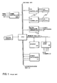
- the Central Processing Unit (CPU) 101 is the basic seat of intelligence in the computer and, as is indicated by its being depicted at the hub of all the other elements, is called upon to control all information transfers between those other elements.
- CPU 101 is connected to memory 102 by memory bus 103, and must control all transfers over memory bus 103.
- System console 104 connects directly into CPU 101, which must control all transfers to system console 104.
- CPU 101 is connected to the external world by I/O bus 105, which connects to I/O controllers 108, through which transfers may be made to I/O devices 109: communications controller 106, through which transfers may be made to communication lines 107; and interprocessor controller 110, through which transfers may be made to other processors 111 comprising the distributed computer network.
- the controllers 106, 108, and 110 may be provided with some limited intelligence to control low-level details of transfers effected through them, but CPU 101 must provide all high-level control, setting up the controllers and overseeing returns of status information from them.
- interprocessor bus 112 may be provided to interface with other processors 111; this may relieve some of the load on I/O bus 105, but does nothing to eliminate the problem of overhead on CPU 101.
- Video RAMs 113 may be provided to contain "bit maps" of screen information for user terminals.
- CPU 101 provides bit map data and stores it in the RAMs in a form in which it may be displayed on user terminals.
- Graphics memory is composed of thirty-two 64K Video RAMs (VRAMs) 113 and is organized into a 1K x 1K x 2 space.
- RS-343A monitor timing allows display of the entire array.
- Palette I/O and other local operations are transacted through "Graphics Space", actually encoded as the IOC Auxilliary Processor (AP) Communication channel.
- AP Auxilliary Processor
- display memory timing and control logic 202 will arbitrate for the Memory Bus 103 as a requestor.
- the 64K double-word video memory 113 is manipulated by the CPU as normal system memory.
- the screen is generated from a logical bit-map packed within a linear array of double-words which are ordered in the classical sense of left-to-right and top-to-bottom. Two bit pixels will be packed left-to-right with their most significant bits toward the double-word most significant bit.
- VRAM random access cycles are essentially identical with those of standard DRAMs. Their unique characteristic is the ability to transfer an entire 256 bit row of internal storage to a serial shift register 203 in one special access. This register may then be clocked independently of further random access activity. Additional controls allow multiplexing four 64 bit sections of this row register to aid in configurability.
- Dot and CRT timing is derived from a local oscillator operating at approximately 44 MHz. Due to the independent nature of VRAM serial clocking, no explicit synchronization with existing memory timing, other than the arbitration for register-transfer cycles, is required. Relatively simple multiplexing is all that is required to pass pixel values to the palette.
- the above capabilities can be satisfied by an intelligent micro-controller 206 (uC), the Intel 8051 being the best choice in that minimal cost and CEQs will result, although an 8031/2732 EPROM implementation is also possible.
- a Memory Bus Arbiter 202 will grant the register-transfer, graphics, and palette cycles requested by the display memory uC.
- Standard protocol will be implemented in a PAL-based state machine.
- ERCC syndrome bits will be generated logically for all reads both as an economical measure and due to the circumstance that VRAM outputs remain tri-stated during register-transfer cycles.
- Microcode will implement AP protocol via UABA references to write palette data and initiate any required commands.
- the Palette 204 is organized as a 4 x 2 x 2 array arranged within a single double-word of storage. Two-bit Palette data written through the AP Graphics Space will encode the desired gray level to be associated with a given pixel value for each phase of the blink clock. Although direct reading of this register is not available, Microcode maintains an image of it in a single scratchpad location.
- the EDH13400 208 is actually a tri-DAC of which only the green channel will be driven. It not only performs sync-mixing, but is capable of direct 75-Ohm drive.
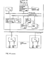
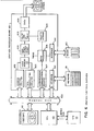
- the system is seen to comprise a central processing unit (CPU 101), memory (102), video interface 320 consisting of video rams 113, video driver circuitry 324, and a video display 322.
- User software 307 and 309 which is resident in memory (102) may include all manner of software entities, including CPU instructions to manipulate the logical displays (311, 313, and 315) or software calls for windowing services.
- Such software calls invoke windowing software 317 also resident in memory (102) which interprets the user's calls and in turn may present to the CPU instructions which will result in carrying out the user's requests or call system software to carry out the user's requests.
- the windowing software 317 may interrogate the display databases 311, 313 or 315 to determine the previous state of the display, and will update the display database so that it reflects any changes brought about by the current call from user software.
- machine language instructions presented to CPU 101 by software are decoded by element 303 which, regardless of whether by "hard-wired” or microcoded means, directs arithmetic and logic unit (ALU) 305 in executing the instructions.
- ALU arithmetic and logic unit
- the descriptive information in display databases 311, 313, 315 is then used to create a new screen bitmap 113, which would then contain a "screen image" of the display screen as it should now appear, reflecting the manipulations called for by the current calls from user software.
- Display interface 324 (regardless of whether by programmed I/O or Direct Memory Access means) reads and processes the bit map to generate appropriate signals to display 322 causing it to display the information specified in bit map 113.
- bit map is used herein by convention, and may denote a character map for a character-oriented display, or a pixel map for a pixel-oriented display:
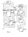
- CPU 101 is no longer configured at the hub of all the other elements.
- Over Local Memory Bus (LMB) 403 CPU 101 can communicate with integrated I/O and system console processor (ISC) 402, and memory control and I-Bus interface (MCU) 401, both of which contain sufficient intelligence to oversee their respective functions without close supervision by CPU 101.
- ISC system console processor
- MCU memory control and I-Bus interface
- MCU 401 determines whether memory locations requested by CPU 101 are in local memory or not; if not, MCU 401 automatically performs the requested memory reference via I-Bus 404 in the memory associated with another computer on the network.
- All memory locations within the distributed system are accessible to any CPU -- a CPU may read from or write to a memory location associated with another CPU on the distributed system with the same facility with which it may access any of the memory locations associated with itself. All memory access requests from a CPU 401 are passed over LMB bus 403 to MCU 401, which determines from the memory address whether the desired location is associated with the local processor (the processor containing the CPU and MCU) or one of the other processors comprising the network.
- MCU 401 accesses the local memory 102 (or video RAM 113, as appropriate) over memory bus 405 performing the requested read or write and obtaining data from CPU 101 over LMB bus 403 (if a write) or passing data to CPU 101 over LMB bus 403 (if a read). If the latter, MCU 401 passes the request over I-Bus 404 whence the MCU 401's of all other processors on the system examine the memory address; the processor having that address within its local memory performs the memory access, the data being passed over I-Bus 404 between the MCU 401 of the processor having the memory address and the MCU 401 of the requesting processor.
- An arbitration scheme is provided to ensure that no processor can monopolize the I-Bus and that no processor can be deprived of the use of the I-Bus. This scheme is based on a rotating priority, wherein the processor that has just used the bus is given lowest priority and must wait till other requesting processors have used the bus before it can use the bus again.
- ISC 402 contains a microprocessor and is provided to relieve CPU 101 of detail-level oversight of data transfers between the computer and I/O devices 109, communication lines 107, and system console 104.
- LMB bus 403 is provided so that communication between CPU 101, ISC 402, and MCU 401 can take place without contention from any of the memory devices 102 or 113.
- VCU 406 is provided ahead of the video RAMs 113 to relieve CPU 101 of much of the detailed work of modifying bitmaps for controlling displays on user terminals.
- VEU 407 may optionally be provided to expand the pixel size from 8 to 24 bits.
- VEU 407 includes additional VRAM chips, but does not result in the creation of more VRAM locations-- it merely expands the size of the existing locations.
- each computer is a 32-bit computer and is embodied on a single 15"x15" printed circuit board.
- Each board contains its own LMB Bus 403 which does not leave the board.
- Each board has a connection to I-Bus 404.
- Each board has a Memory Bus 405 which may leave the board and connect to optional expansion memory and video memory boards; up to 2 MBytes of memory may be accommodated on the processor board and are connected to Memory Bus 405; additional memory and video memory boards may be connected to the processor board's Memory Bus 405 to expand each computer's memory capacity.
- I-Bus 404 is made up of backplane wiring and interconnects all the computers plugged into the cabinet to form a distributed computer network.
- the sixteen computers may share a total memory space of 512 MBytes. As described above, any of the computers may access any location of the 512 MBytes, which may thus be regarded as a "global address space".
- the Memory portion of the CPU contains the main memory control unit (MCU 401) and 2 Megabytes of main memory 102 itself.
- the MCU 401 also provides the control for an expansion memory bus 405 (called the MEM Bus) and the control for the global I-Bus 404.
- the MEM Bus 405 is also the connection for bit mapped video screens that are attached to the main memory address space.
- the only communication path between the CPU portion or I/O portion and Memory portion of the board is the LMB 403.
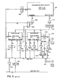
- the Memory portion is entirely controlled by two gate arrays (see figure 5): CMOS-MEM gate array 561 and Bipolar-MEM gate array 562. These two gate arrays are basically traffic directors and error checking devices which control all the interactions that take place among the LMB 403, and I-Bus 404 and the MEM Bus 405.
- the LMB 403 and the I-Bus 404 are the two busses that can initiate memory operations.
- the LMB 403 initiates all local memory accesses while the I-Bus 404 initiates all accesses of this particular node from other global nodes.
- the MEM bus 405 is essentially an internal bus to this memory portion which carries the actual address and data of the local RAM's themselves. This bus is "raw", unaligned, uncorrected data which is stored in the RAMs themselves.
- This MEM Bus has expansion capability so that up to 16 Mbytes can be addressed by this MCU (the two gate arrays) without adding more control. Thus, the MEM bus goes off-board so that additional memory can be added either in the form of standard DRAMs or in the form of memory mapped graphics.
- the MCU 401 (combination of CMOS 561 and Bipolar MEM 562 gate arrays) recognizes the start of the memory operation. It then makes a determination of whether the reference was a local reference - i.e. to this node - or a global reference. Assuming it was local, the MCU generates the proper RAS and CAS (row address and column address) lines to access the required data. (The RAS and CAS lines are part of the MEM Bus 405). Either the memory array on the board itself (2 Mbytes) or an external expansion memory on the MEM Bus 405 will respond with the data.
- the MCU 401 now directs that data back onto the LMB 403 and signals the processor 101 that the data is available. If the data required aligning or correcting, the MCU 401 would have taken the data into the gate arrays themselves, manipulated it as required, and rebroadcast the data back onto the LMB 403 prior to signaling the processor 101.
- the MCU would not have issued the reference on the MEM bus 405. Rather, the MCU would have begun arbitrating and re-initiating the reference onto the I-Bus 404.
- the responding I-Bus node 111 will return aligned, corrected data back via the I-Bus 404 at which time the MCU 401 will direct the data back onto the LMB 403, buffering the data as necessary.
- VCU 406 provides high resolution color graphics (1280 x 1024), using 8 bits per pixel.
- Video Expansion Unit (VEU) 407 may optionally be included to expand the pixel size to 24 bits, giving the effect of a 24-bit VCU 406.
- VEU 407 includes augmentation of VRAMs 113; this does not provide additional VRAM locations, but expands the size of the existing locations from 8 to 24 bits.
- VCU 406 drives a 60 hertz non-interlaced 19" color monitor.
- the video outputs to the monitor are RGB (RED-GREEN-BLUE) sync-on-GREEN with 75 ohm drive impedance.
- Pixel data retrieved from VRAMs 113 are not written to the screen directly, but are input to a table lookup function.
- the table contained in a separate RAM and known as a "palette", outputs a 24-bit number.
- Eight of the 24 bits are converted from digital to analog to provide the RED video signal, eight provide the BLUE, and eight provide the GREEN. There are thus 2 ** 24 (two to the 24th power) or 16 million colors which can be displayed.
- 8-bit pixels can display any 256 of the 16 million colors at any given time; the selection of which 256 may be altered by reloading the palette RAM.
- 24-bit pixels can display any of the 16 million colors; the correspondence of pixel value to color may be altered by reloading the palette RAM.
- VEU 407 must be used in conjunction with VCU 406 and connects to VCU 406 via 44 signals on the backplane. It provides an additional 16 bits per pixel bringing the total bits per pixel of the graphics display from 8 to 24. VEU 407, having circuitry analogous to that in VCU 406, will not be described in detail.
- Pixel data from the host computer may be written directly into VRAMs 113, or may be combined according to various Boolean rules (discussed later) with data previously in VRAMs 113.
- VCU 406 may be operated in "pixel mode” or "plane mode".
- Pixel mode provides more flexibility, since any of a great number of colors may be drawn at any screen position, but requires the host to forward every bit of every pixel of a desired display.
- Plane mode is provided to enhance performance, at the expense of limiting the number of colors that can be displayed for a given palette loading to 9 for VCU 406/8 or to 25 for VCU 406/24.
- Plane mode effects "planes" or “layers” of displays (eight planes for VCU 406/8, 24 planes for VCU406/24) wherein the color of each plane need be specified only once, “higher” planes may obscure “lower” planes, and the host need only send a single bit (denoting "ON” or "OFF") for each pixel position of each plane. For example, if it is desired to display a bar graph in which:
- the desired bar graph is now displayed on the screen. Although some of the data is obscured (namely, the portions of the yellow bars that are under red labels; the portions of the green grid that are under yellow bars; the portions of the blue background that are under green grid lines) it is still present in VRAMs 113 and will again become visible when the overlaying data is removed. For example, if zero-bits are sent to the third plane, thus erasing the red labels, the yellow bars will again be fully visible with no need to reconstruct any portion of them; likewise, if zero-bits are sent to the second plane to erase the yellow bars, the green grid will again be fully visible without having to reconstruct it.
- VCU 406 and VRAMs 113 are contained on a circuit board (Graphics Processor Board 301) which is a 15" x 15" 6 layer board with etch width of 8 mils and etch spacing of 8 mils.
- the board contains the following major components:
- NMIs non-maskable interrupts
- the mouse can interrupt the host as fast as every 33 milliseconds.
- Servicing of the mouse, which includes cursor plotting/replotting, should require no more 50 microseconds out of every 33 milliseconds of time. This is a total of .15% of the host's cpu time when the mouse is moving, which relatively speaking, is not often.
- the keyboard constantly interrupts the host at an interval of 80 milliseconds.
- the time required to service the keyboard when it is idle is about 25 microseconds, a total of .03% of the hosts cpu time. If the keyboard is not idle, the time to service it is about 400 microseconds. With a typist who can type 60 words/minute (a word being 6 characters), the interrupt load is equal to about .12% of the hosts cpu time.
- VCU 406 can be used to pace the color palette updates.
- VCU 406 only updates palettes during vertical blanking. It takes 6 frames to fully update the 3 256-color palettes. Multiple attempts by the system to update the palettes in less than one frame will not be realized.
- the system can use the vertical blanking interrupt to indicate that VCU 406 has updated the palettes, and to issue another update if required. Since this function can be done via setting a flag, the time to service the interrupt is considered negligible.
- Total load on the system worst case, including both mouse and keyboard, is estimated to be approximately .27% of the total CPU time.
- pixel data is sent from the host CPU over Memory Bus 405, is processed by the Graphic Data Processors 714, and eight-bit pixels are stored in "bit map" form in VRAMs 113.
- GDPs 714 have the capability, in response to commands from the the host CPU, to extract bit map data from VRAMs 113, perform manipulations upon it, and return it to VRAMs 113.
- Writing to VRAMs from the host is known as an "external” access”; the latter case is called an “internal” access.
- Circuitry 604 extracts bit map data from VRAM's 113 and transforms each pixel to a desired video representation as directed by palette 609 under control of palette lookup table 605.
- Digital- to-analog converters (DACs) 606 transform the video representations to red, green, and blue video signals which are forwarded to the video monitor for display.
- Plane mode data follows essentially the same path as pixel mode data, but is handled differently, as shown in Figure 8.
- a representation of the character "A" (element 815) is shown as it might appear in a "font” of characters (fonts, well known to those in the art, may be thought of as prestored bitmaps of often-used graphic entities).
- the prestored plane-mode (one bit per pixel) bitmap for "A" is shown as element 816.
- the color denoted by foreground register 819 will be displayed at the corresponding screen position; where it contains a 0, the color denoted by background register 818 will be displayed.
- the discussion of the bar graph example in section 5.1 did not consider use of these registers; they enhance flexibility by permitting, for example, red labels on a black background on the yellow bars. It is assumed here that the background register contains a value denoting the yellow of the bars and that the foreground register contains a value denoting the desired red of the labels.
- the video memory (VRAMs 113) contains video information which is continuously displayed on the screen.
- the smallest picture element that is addressable in the video memory is called a pixel.
- Each pixel contains information that corresponds to a value that the pixel can take on.
- a pixel is represented by 8 bits of video memory, and can take on any one of 256 possible values.
- a pixel is represented by 24 bits of video memory, and can take on any one of 16,777,216 (written as 16M for future discussion) possible values.
- This section of the video memory can be used to store temporary pictures, icons, character fonts, or small windows of data.
- Each bit of the pixel is called a 'plane'.
- VCU 406/8 When configured as an 8 bit per pixel controller (VCU 406/8) there are 8 planes.
- VCU 406/24 When configured as a 24 bit per pixel controller (VCU 406/24), there are 24 planes.
- the pixel plane bits are passed to the address field of a high speed RAM lookup table.
- the data returned by the RAM is then passed to the video output stage.
- This table allows the pixel information stored in the video memory to be redefined before being displayed on the screen.
- This RAM is called the color palette.
- VCU 406/8 8 bits of information are placed on the RAM address lines and 24 bits of data are returned. Because each pixel is 8 bits wide, it can take on any one of 256 values.
- the colors represented by the values can be chosen from a range of 16,777,216.
- VCU 406/24 with respect to the color palettes, is essentially 3 VCU 406/8 designs in parallel.
- VCU 406 is designed to read and write the video memory on pixel boundaries. To accomplish this, VCU 406 manipulates the data internally. Furthermore, on write cycles, VCU 406 performs a read-modify-write cycle internally. MCU 406 , the M-bus controller, is also capable of performing read-modify-write cycles, but cannot manipulate the data in the same manner as VCU 406. VCU 406 expects only simple reads and writes via the M-bus. If MCU 406 performs a read-modify-write to VCU 406, indeterminate results will occur.
- VCU 406 is capable of the following types of video memory accesses:
- the format in which the data is packed is BLOCK form - the 32 bit data word contains 4 consecutive 8 bit pixels for VCU 406/8; and 1 right justified 24 bit pixel for VCU 406/24 for video memory accesses.
- a special character write contains 32 consecutive pixels in a doubleword access and is independent of the bits per pixel.
- Video memory to video memory accesses do not use the M-bus.
- INTERNAL READ data is read from the video memory and stored in an on-board register.
- the transfer of data is not bandwidth limited by the M-bus to 32 bits per access; but rather limited to the bandwidth of the video memory data lines.
- VCU 406 it is 32 times the number of planes per pixel. This yields a transfer rate of 256 bits per transfer for VCU 406/8 and 768 bits per transfer for VCU 406/24. In both cases, this translates to 32 pixels per transfer.
- the SOURCE registers are normally used as pointers to a row and a column of the window to be moved or drawn.
- VCU 406 can use either pair of registers to read or write. This allows for easy handling of block moves and logic operations from video memory to video memory.
- window moving in either the X or the Y plane oan be accomplished much more efficiently because only one coordinate address needs to be sent after the initial X and Y address is loaded.
- SOURCE and the DEST registers can be used for reading and writing. Labels "source” or “dest” are used for clarity only, although SOURCE register normally holds the top right coordinate of the window to be read and DEST register normally holds the top right coordinate of the window to be written.
- PIXEL operations may be used to draw lines, circles, and other pixel-by-pixel graphics efficiently.
- Pixel read and pixel write are just special cases of BLOCK READ and BLOCK WRITE respectively.
- All accesses are double word accesses. However, if the pixel enable register contains a value of 00000001 (hex) then on a host write access, a pixel write is accomplished. The pixel to be written must always be right justified. Similarly, on a host read, the right most pixel of the double word read from the video memory is the pixel addressed, the rest of the pixels must be masked out by the host CPU. Note that the PIXEL ENABLE register is used by VCU 406 only on a write cycle.
- PIXEL accesses require the setup of the following registers:
- a double word access will access either 4 consecutive pixels on VCU 406/8 or 1 pixel on VCU 406/24.
- each pixel is 8 bits wide, so 4 pixels will fit into a double word.
- each pixel is 24 bits wide, so only 1 pixel will fit in a double word. This 24 bit pixel is RIGHT JUSTIFIED in the 32 bit double word. Note that, setting or clearing of the video memory is faster if a special character write access is performed instead.
- BLOCK addressing may be used when it is required to move or draw a large rectangular blocks of graphics memory more efficiently.
- CHRBLT, 2DLINE,and BITBLT instructions use BLOCK transfers. Note that BLOCK accesses are NOT limited to double word boundaries of pixels, but are limited to pixel boundries.
- VEU 407 is very similar in hardware design to VCU 406. The following paragraphs describe those differences.
- VEU 407 There is no address generation, refresh control, or X and Y source and destination register sections on VEU 407.
- the address that goes to the video RAMs is passed via a cable to the VEU 407 board from the VCU 406 board.
- VEU 407 There are two video output chains (shifters, etc.) and twice as much memory (128 video RAMs) on VEU 407 as there is on VCU 406. Note that this memory does not yield any additional locations, but expands the size of the existing locations. There are only two DACs on VEU 407, one per video output stage.
- VCU 406 There exists a jumper cable that is connected on the backplane when both VC U 406 and VEU 407 are present in a system.
- This cable passes signals from VCU 406 to VEU 407 and vice-versa.
- One of the signals on the cable tells the VCU 406 board that a VEU 407 is connected so that it (VCU 406) configures itself appropriately.
- the RED gun and GREEN gun cables are connected to the VEU 407 slot.
- the BLUE gun, keyboard cable, and mouse cable are connected to the VCU 406 slot.
- CPU is meant to be the data processing system, and includes, but is not limited to, the parts of the data processing system depicted in fig. 9.
- the method of the present invention uses significantly less of the processing power of a given machine, or permits implementation of windowed displays on a smaller, less powerful machine than is possible for a prior art implementation.
- the method of the present invention is depicted in fig. 4, but fig. 4 does not purport to depict all elements of a data system, but only those elements necessary to generate and produce displays.
- the data system is again seen (see fig. 4) to comprise a CPU (101), memory bus controller and interface (401), a memory bus (404), memory (403), a video control unit (405), a video expansion unit (406), video rams (407) and a display (408).
- the display is a pixel-oriented video monitor and not a character-oriented terminal.
- a display interface is used that is appropriate to drive the video monitor.
- User software is not constrained to software calls for manipulating the displays, but may now also contain instructions which will directly stimulate CPU 201 for that purpose.
- User software is always constrained to manipulate logical displays, which may or may not be on the physical display.
- user software 311 must make software calls to a piece of system software called the window manager 317, to produce form descriptors. This is usually not a frequent operation, and can be slow. A user may not provide her own form descriptors, but must have the window manager provide them for her. The user then uses a unique form identifier returned to the user by the window manager that represents the form descriptor created for her. This is necessary in a multi-user, multi-program, or multi-process environment to arbitrate among the various users, programs, or processes that are contending for window space on the same physical screen.
- Each user graphics instruction (for writing into windows) are presented by user software (307, 309) to CPU (101) where they are interpreted by the microcode unit (303), which in response to each instruction fetches an appropriate sequence of microinstructions to direct ALU (305) in performing the instruction.
- Each such user graphics instruction must contain a user form identifier.
- the current operating system key for the user currently running on the CPU. (The operating system key was set when the user was given the CPU via the SBR management instructions. In a different embodiment, this key can be generated differently, as long as it uniquely identifies all users in the system and can be agreed upon by the hardware and system software).
- the microcode searches the forms entry cache looking for a matching form identifier/operating system key pair.
- a forms cache miss fault is generated, basically calling system software to resolve the fault.
- the operating system must then search its list of valid forms for this particular user to determine if a new form must be loaded into the cache (using the WGLFORM instruction) or if the user attempted to reference an illegal form.
- the form descriptor address is gotten from the form id cache.
- the form descriptor address is then used to see if the form descriptor is encached in the form descriptor cache. (In the preferred embodiment, the form descriptor is actually encached both on the CPU 101 and the Video Control Unit 406. In other embodiments, the descriptor may be wholly encached on either the CPU or VCU, or not cached at all. Also note, that other descriptors, related to the form such as the rectangle, attribute and cursor descriptors are also cached to differing degrees). If the form descriptor is not cached, then it is read from memory 102 into the form descriptor cache. After the form descriptor is in cache, the graphics instruction can proceed.
- This cache can be a high speed scratch pad memory used by the CPU, or it can be wholly implemented on a graphic processor board.
- Some form of caching will be necessary to store the form id, operating system key, form descriptor address triples to avoid faulting to the system software on every user graphics instruction. This caching could be a known location in main memory, or high speed scratch pad space in the CPU.
- the reading of the form into the internal cached form consists of calculating screen-global coordinates from window-local coordinates provided by the system in the form descriptor. (The user is not required to know where on the screen her window is located, and can only find out by asking the window manager software).
- a window positioned on a screen is depicted.
- a user-specified origin "O" (1007) (the user may specify coordinates in the window relative to this origin) and a point "P" (1008) at which the user may wish to operate.
- Listed on fig. 10 are the global coordinates of the corners of the screen, and the global and local coordinates (relative to the upper left corner (ULC) of the window) of points of interest of the window: its four corners E,F,G,H.
- the system is required to specify the height and width of the window (in pixels), and the local coordinates relative to the user's origin "O" of the window's ULC. Note that this implicitly specifies the location of the origin "O".
- Fig. 11 depicts a form descriptor in system form.
- the transformation spoken of consists in calculating and filling in the global coordinates of the window's ULC (1009 and 1010) and a pointer to global 0,0 (1007). Since the form descriptor can now be encached as a forms cache entry, there is no need to recalculate such information on subsequent references to the same window, unless the window's global ULC changes.
- Every bitmap employs a global coordinate system within which individual windows are allocated.
- Each form defines its own local (internal) system that is independent of the location of the window within the containing bitmap.
- Display-affecting instructions are written in terms of local coordinates; translation to global coordinates is performed when the instructions are executed.
- a form descriptor contains both local (1103, 1104) and global (1101, 1102) designations of the form's Upper Left Corner (ULC), point E (1003).
- the encached form descriptor supplies vectors AE (E's global coordinates 1101,1102) and OE (E's local coordinates 1103, 1104). Instruction inputs supply vector OP (P's local coordinates: XL,YL relative to the user supplied origin 1007).
- the vector AP is calculated internally.
- the cache then always contains the transformed versions of the "n” most recently used forms descriptors. This can greatly accelerate execution, since in practice many forms will often be used repetitively. (The determination of the value of "n” is left to the designers of a particular embodiment).
- bitmap 1007 contains an image of what is to be displayed on the screen
- execution of the present instruction may be regarded as complete when the bitmap is updated to contain the new display information specified by the current instruction.
- Translating the bit map 1007 to a visible display is a function of display interface 324, the timing of which is asynchronous to the timing of instruction execution.
- bitmap 1007 is contained in VRAM's (video random access memory chips). Depending on the particular embodiment, the VRAM's may or may not be accessible to the ALU just as any other portion of main memory.
- the method will not permit a user to write outside of the window he has referenced.
- the system software is responsible for defining the size of the user's window, by specifing in the form descriptor the bounding rectangle 1105, 1106, 1107, 1108 that the user's references must stay within. For example, if a user instruction specified a horizontal line 400 pixels long in window 1002 that is only 250 pixels wide, only that portion of the line that fits within the window is written to the window 1002, and the rest is ignored. This is known as "clipping". The user is NOT informed that the clipping has been performed; further, the user does not need to know this. If the user was to be informed, then parallel operation of the graphics subsystem would greatly be limited, since the CPU would have to 'wait' for the graphics instruction to nearly complete to determine if clipping information needs to be returned.
- rectangles must always be rectangular in shape -- i.e., the method does not allow consideration of the occluded rectangle and the L-shaped remainder, but requires division of the L-shaped remainder into two rectangles, B2 and B3.
- the system software creates a descriptor describing each pane. This descriptor is known as a rectangle descriptor. Form descriptors describe the entire window, whereas rectangle descriptors describe only an area of the window. See appendix B, section 1.4, for a detailed description of the rectangle description.
- a form descriptor for a window essentially comprises a list of pointers to the rectangle descriptors that make up that window.
- these pointers are kept by using a linked list, anchored in the form descriptor for the window, using physical addresses. It is interesting to note that the form descriptor can easily change shape and size since a size field is part of the descriptor, and that only the operating system software uses the form descriptor, not user software.
- fig. 13 which depicts the forms descriptor 1301 for Window B 1201 that reflects the occlusion situation depicted in Fig. 12, it is seen that the window has been broken into three rectangles (or panes) 1306, 1308, 1310.
- the window manager software when told to move window B 1201 over the top of window A 1202, divides window B 1201 into the proper number of rectangles, creating new rectangle data descriptors, allocating virtual bitmap space (more properly, virtual rectangles) and copying the data from the physical display into memory as necessary.
- the triple form identifier / os key / form descriptor address is purged from the CPU; then any references the user attempts to make will result in a cache miss fault.
- the window manager (with help from system software) will pend the user's path (by not reloading the cache and resuming the fault) until the window manager has finished modifying the window.
- a cursor 1207 is shown. Since the cursor is not part of a user's window proper, users do not need to be aware of where it is. Consequently, drawing over the top of the cursor should not destroy it, or make it invisible. Users can still have 'user' cursors that are not allowed to leave the window. This is very useful when providing a terminal like interface within a window.
- descriptor for a window is a pointer 1109 to a cursor descriptor 1303.
- Cursors may be visible or invisible; if invisible the CPU knows it can safely ignore any intersections.
- microcode When an operation initiates, microcode must determine whether it can do the operation, and whether it can handle the forms on which it must operate. If the answer is no in either case, the instruction must fault to system software before it produces any side effects.
- a fault handler address is supplied in segment zero. The fault handler will determine what operation must be performed (load a form descriptor, moving a cursor, provide attribute information, or invalidate a reference), by using user and privileged instructions if necessary.
- the invoking program is resumed via WDPOP. For more details, see Appendix B, section 4.
- system software will receive the fault, it may then pass that information onto the window manager to handle.
- the window manager does not need to be a part of the system software proper, but is nonetheless, still a trusted part of the operating system.
- microcode When a graphics instruction starts, microcode must determine if the instruction is defined. If it isn't, an Undefined Instruction Trap (UIT) is performed and control is passed to the user provided Emulator routine.
- UAT Undefined Instruction Trap
- This routine's address is the 2nd and 3rd words of the instruction, which holds a program counter-relative offset (non-indirectable), of a software emulator/fault handler.
- the process performs a LPSHJ to the routine.
- the emulator handler can then emulate the function, and return via an WPOPJ instruction. Recursive traps are thus supported implicitly.
- the present embodiment uses a pixel value as simply an index into a palette.
- a palette is a special hardware map, which translates pixel values to (digital) beam intensities. Privileged instructions exist to set and retrieve pixel-to-color translations, i.e., load and store the palette.
- the palette Since the palette is a resource to be shared by more than one user, it must be protected by the system. This is accomplished by making the palette instructions privileged. System software is responsible for dividing the palette up into as many pieces as possible so that all users sharing the physical device can have as many useful 'colors' as possible.
- the form descriptor When the form descriptor is created for the user, the range of possible palette entries that the user can use is specified by bit mask in the forms descriptor called the op mask.
- the CPU When the user writes a pixel (via a write pixel or bitblt instruction) onto the physical bitmap, the CPU masks the users pixel bits by using this op mask, by masking the cooresponding pixel on the physical bitmap using the one's complement of the op mask, then ORing the user's pixel with bitmap pixel. If a combination rule was specified, or if the user specified a global operation mask, this is applied. (NOTE that masking is a transitive operation, leaving the designers to change the order). Optimizations are possible due to different combination rules and attributes the user has specified. See combinations rules and attributes in appendix A for more details.
- the system software must precharge, by using an WGRFLOOD instruction, each portion of the physical bitmap with the user number before the user can effectively use that area. In future embodiments, this could be moved into hardware, by including the user number to the forms descriptor.
- a side effect of this mechanism is that when rectangles are occluded, and moved off the physical bitmap onto a virtual bitmap, only the exact number of bits per pixel that the user can use is required. Using the previous example, then when a rectangle is virtualized, it only requires 4 bits/pixel, half the space required when on the physical bitmap.
- the palette can be split into asymetric partitions by giving different users different size masks. For example, if one user requires 32 colors, then it would have a five bit mask. Using this technique, the only real restriction is that the user always receives a power of two colors. This makes sense, since the user must always use a whole number of bits to represent a pixel.
- the present embodiment provides a blink clock.
- the blink clock provides a stimulus to switch between two palettes with a 50% duty cycle at a fixed rate of about 1.0-1.5 Hz. Entries in the two palettes are specified separately. This allows a given pixel value to alternate between two colors (or levels of intensity on a mono-chrome display).
- the chart below shows some of the effects possible when using this palette scheme for two-bit pixels.
- Attributes are stored in the attribute descriptor 1305, 1312 whose address is kept in the form descriptor 1110. Individual attributes are referenced by an index number into the attribute descriptor. Currently, all attributes are 32-bit quantities. These attributes are set by the WGWRATTR instruction, and read by the WGRDATTR which are non-privileged instructions.
- each bit in the source pixel VALUE is combined with the corresponding bit in the destination pixel VALUE, to form the new destination pixel VALUE.
- a standard Boolean function is used to specify the logical operation used for each bit position.
- the operation mask selects which pixel bits are modified by the operation. A zero means “do not do anything to this bit,” while a one means “operate on this bit using RULE.”
- the COMBINATION RULE is applied on a bit-by-bit basis to each bit in the source pixel and destination pixel.
- the RULEs are defined as follows: Those RULEs with a dash in the interpretation column are seldom used and have no particularly meaningful interpretation. (The exclusive nor, XNOR, operation is also known as the equivalence, EQV, operation.)
- Linestyle word combined with the Line Control word is a way of drawing other than solid lines.
- the line style word is specified as a bit string of length 32, it controls which color (foreground or background) to use when drawing the line. For each draw position, the leftmost bit in the linestyle is examined. If set, the foreground color (pixel) is planted; if clear, the background color (pixel) is planted. The linestyle is rotated left one bit position, and the next draw position is computed.
- the line foreground color, line background color and line control word are set by using the WGWRATTR (write attribute) instruction.
- WGWRATTR write attribute
- the Line Control word is used to determine whether to use the foreground and/or background colors, and to join multiple lines. In the current embodiment, only four line control characteristics are defined: suppress leading or trailing pixel, suppress foreground or background color.
- a font organization has been chosen that uses one bit per pixel bitmap. Character drawing is controlled in a manner similar to the linestyle process. There is a character foreground and background color as well as a character control word.
- a character drawn by WGCHRBLT from the character bitmap onto the actual target bitmap.
- the bit is set the foreground color (pixel) is planted; if the bit is reset the background color (pixel) is planted onto the target bitmap.
- the character control word is used to determine whether to use the foreground and/or background colors. For more details on character attributes see Appendix A, section 1.4.
- the Character Block Transfer (WGCHRBLT) instruction allows for arbitrary font specification.
- Drawing a line is an important part of technical computer graphics. It is used in CAD/CAM packages, architectural design packages, and business graphics packages. Since this operation is performed so often, special instructions are provided. Both continuous (LINESEG) and incremental (BRESENHAM STEP) forms of line drawing are included. Lines can be drawn closed, half-open, or fully open. The actual algorithm must be reversible so as to make things such as line erasure precise.
- This access method deals with individual pixels and rectangular areas of them. It can serve as the foundation of higher-level accessing methods, so that users can create their own display manipulation instructions (for image manipulation, conic section generation, etc). Read Pixel and Write Pixel operators allow direct access to pixels. Although only these two operations are strictly necessary to do the job, higher level operations are much more common.
- a Bit Block Transfer (often abbreviated 'BITBLT') operator is a very useful pixel-level operator. It is essentially a rectangular combination and assignment function. This is done especially when scrolling windows, moving windows around, creating and destroying windows that obscure other windows. A special rectangular fill operation is also useful for dealing with clearing screens and repartitioning windows.
- BITBLT is the only operation that takes two forms, since certain restrictions are placed on source and target forms. Source logical pixels will be padded or chopped to conform to the target form's parameters.
- All Graphics Instructions share a common instruction stream format.
- the first 16-bit word of all such instructions is octal 107151 (hexadecimal 8E69, Nova ADDOL# 2,0,SKP).
- the next two 16-bit words hold a program counter-relative offset (non-indirectable), of a software emulator handler.
- the fourth 16-bit word contains a small, unsigned integer sub-opcode that specifies the particular function to be performed.
- the instruction set is broken into two parts: privileged (system) instructions, and non-privileged (user) instructions.
- privileged system
- non-privileged user instructions.
- the following table lists the mnemonic, brief description and the decimal sub-code.
- Non-privileged instructions See appendices A (non-privileged) and B (privileged) for detailed descriptions of these instructions.
- Attributes are stored in the Form Descriptor and are referenced by an index number. Currently, all attributes are 32-bit quantities. These attributes are set by the WGWRATTR instruction
- the operation mask and combination rule are attributes used to specify how pixels are to be combined for any instruction that writes to a FORM. These attributes are set by the WGWRATTR command.
- each bit in the source pixel VALUE is combined with the corresponding bit in the destination pixel VALUE, to form the new destination pixel VALUE.
- a standard Boolean function is used to specify the logical operation used for each bit position. This function is called the COMBINATION RULE, or simply RULE.
- the OPERATION MASK selects which pixel bits are modified by the operation. A zero means “do not do anything to this bit,” while a one means “operate on this bit using RULE.”
- the COMBINATION RULE is applied on a bit-by-bit basis to each bit in the source pixel and destination pixel.
- the RULEs are defined as follows: Those RULEs with a dash in the interpretation column are seldom used and have no particularly meaningful interpretation. (The exclusive nor, XNOR, operation is also known as the equivalence, EQV, operation.)
- DEST_PIXEL [OPERATION_MASK AND (SOURCE_PIXEL RULE DEST_PIXEL)] + [OPERATION_MASK AND DEST_PIXEL]
- the visible effect of applying a RULE during an instruction depends on the assignment of COLORs to the VALUEs of the source and destination pixels.
- LINESTYLE together with the LINE CONTROL WORD are used to give a line a texture.
- LINESTYLE is a string of 32 bits that define a pattern (solid, dotted, dashed, etc.). As WGPLINE draws each pixel, it looks at each bit in the LINESTYLE, going from the most significant bit (MSB) to the least significant bit (LSB). If the selected LINESTYLE bit is 1 for a given pixel, then the pixel is planted with the LINE FOREGROUND COLOR. If the selected LINESTYLE bit is 0 for a given pixel, then the pixel is planted with the LINE BACKGROUND COLOR. When the LSB of the LINESTYLE is reached, the processor returns to the MSB of the LINESTYLE. This process starts at the first pixel of the the first line segment, to the last pixel of the last line segment.
- the LINE CONTROL WORD is used to suppress the FOREGROUND and/or BACKGROUND colors when drawing a polyline. It is also used to suppress the initial and/or final endpoint of the polyline. Suppression of a pixel means that it will be left unaffected by the instruction.
- the WGCHRBLT CONTROL WORD is used to suppress the FOREGROUND and/or BACKGROUND colors when character plotting.
- the GIS provides a mechanism for future expansion to include instructions in addition to those listed here. If the processor encounters a graphics instruction with an unknown sub-opcode or if it cannot process the instruction for some other reason, it performs an unknown-graphics-instruction trap. This trap makes the processor perform an LPSHJ instruction function. Then, the undefined graphics instruction can be emulated by software, or some other appropriate action can be taken. Return from software is by the WPOPJ instruction.
- Each GIS instruction has an emulator associated with it.
- the address of this emulator is given as a PC-relative displacement in the instruction itself (Bits 16-47).
- the processor pushes PC+4 on the wide stack. Calculates the effective address of the emulator routine. Loads the PC with the effective address. Continues sequential operation at the word addressed by the updated PC.
- All GIS instructions are interruptable and restartable, with an interrupt latency of about 15 microseconds.
- a GIS instruction saves their current state on the wide stack, and takes the interrupt, storing the program counter value for the currently executing GIS instruction in locations 2 and 3 of segment 0.
- Control passes to the address specified by location 1 of segment 0.
- Bit 2 (IRES) of the Processor Status Register (PSR) is set to 1 when a GIS instruction is interrupted.
- AC1 contains the key to the FORM DESCRIPTOR of the FORM containing the pixel.
- AC2 contains a pointer to the X and Y coordinates of the pixel in the FORM.
- ACO contains the pixel VALUE as a 32-bit number, right justified and zero extended; otherwise, ACO is unchanged.
- ACO contains the right-justified VALUE to be written into the FORM.
- AC1 contains the key to the FORM DESCRIPTOR of the FORM containing the pixel.
- AC2 contains a pointer to the X and Y coordinates of the pixel in the FORM.
- This instruction uses the OPERATION MASK and COMBINATION RULE when planting pixels.
- ACO contains the right-justified VALUE to be written into the FORM. This is an nonnegative 32-bit integer.
- AC1 contains the key to the FORM DESCRIPTOR of the FORM containing the pixel(s).
- AC2 contains a pointer to the packet describing the rectangular area in the FORM.
- This instruction uses the OPERATION MASK and COMBINATION RULE when planting pixels.
- ACO contains the number of line segments in the poly line
- AC1 contains the key to the FORM DESCRIPTOR of the FORM to draw the line segments in.
- AC2 contains a pointer to a packet containing coordinates of two or more endpoints.
- This instruction uses the OPERATION MASK and the COMBINATION RULE when planting pixels.
- ACO contains the key to the source FORM DESCRIPTOR.
- AC1 contains the key to the destination FORM DESCRIPTOR.
- AC2 contains a pointer to the packet describing the rectangular area in the source and destination FORM.
- a RECTANGLE is defined by a POINT specifying the upper lefthand corner and the X and Y EXTENT of the rectangle within a FORM.
- the RECTANGLE is a list of 2 signed and 2 unsigned 32-bit integers.
- the X-coordinate is the first double word in the list
- the Y-coordinate is the second
- the X EXTENT is the third
- the Y EXTENT the fourth.
- the source RECTANGLE must be contained within the source FORM and must fit inside the destination FORM when moved. If it does not lie entirely within one of the FORMs, the WGBITBLT instruction will cause the RECTANGLE to be clipped so that it does fit in either FORM. This instruction will not write to pixels on the FORM that are write inhibited.
- This instruction uses the OPERATION MASK and the COMBINATION RULE when planting pixels.
- the SOURCE FORM must be 1-bit per pixel.
- ACO contains the key to the FORM DESCRIPTOR of the SOURCE FORM.
- AC1 contains the key to the FORM DESCRIPTOR of the DESTINATION FORM.
- AC2 contains a pointer to the packet describing the rectangular area in the source and destination FORM.
- This instruction uses the OPERATION MASK and the COMBINATION RULE when planting pixels.
- the source RECTANGLE must be contained within the source FORM and must fit inside the destination FORM when moved. If it does not lie entirely within one of the FORMs, the WGCHRBLT instruction will cause the RECTANGLE to be clipped so that it does fit in either FORM. This instruction will not write to pixels on the FORM that are write inhibited.
- ACO contains the attribute index.
- AC1 contains the key to the FORM DESCRIPTOR.
- AC2 contains a word pointer to store the attribute.
- ACO contains the attribute index.
- AC1 contains the key to the FORM DESCRIPTOR.
- AC2 contains a word pointer to read the attribute from.
- the data structures described here constitute a contract between operating systems and microcode for implementing GIS II. This set of information is the sum total required by microcode from operating systems.
- An operating system can determine that GIS II microcode exists on the system. If an operating system is only concerned with the existence or non-existence of GIS II, it can attempt to issue a GIS II instruction (WGPFORMS is fairly harmless). If the instruction generates a UIT (Unimplemented Instruction Trap) or transfers control to its error handler, the operating system can assume that GIS II does not exist on the system. If the instruction executes, the operating system can assume that GIS II does exist. If an operating system is concerned with the level of GIS II support (which instructions are supported, what level of optimization exists, etc), there is currently no way to find this out.
- UIT Unimplemented Instruction Trap
- the maximum size of any data structure is one page.
- a form is the object upon which all GIS operations are performed.
- the Form Descriptor describes the form itself and points to related databases (cursor descriptor and attributes).
- the Form Descriptor is created in response to a user request.
- the Bounding Rectangle encompasses all rectangles on the rectangle list for the form.
- the ULC of the bounding rectangle is equal to the ULC of the uppermost, lefthand rectangle in the rectangle list.
- the extents of the bounding rectangle are the sum of the extents of the rectangles in the rectangle. list. Tiling a form with rectangles is described in the next section.
- the Form Mask defines the pixel depth of the bitmaps associated with a form. For a bitmap with "n" bits per pixel, the low-order "n” bits of the Form Mask are set to one. The remaining bits in the Form Mask are set to zero.
- the Form Mask is ANDed with the Operation Mask (contained in the Attribute Block) to produce a mask that determines which bits within a pixel should be operated upon.
- the ULC of the virtual bitmap always corresponds to the ULC of the form, regardless of the local coordinate system established for the form.
- the form has only a physical bitmap associated with it, the virtual bitmap portion of the Form Descriptor will be filled with zeros.
- An "empty" bitmap description will never be used by microcode so long as no rectangles on the form's rectangle list refer to the non-existent bitmap. If a rectangle does refer to a non- existant bitmap, the results are undefined. Microcode will probably trap.
- Attribute Block Values such as foreground color and line style are stored in the Attribute Block. Initially, the Attribute Block is filled with a set of default values. All of these values can be examined by the user with the WGRDATTR (Read Attribute) instruction and altered with with the WGWRATTR (Write Attribute) instruction.
- the Attribute Block is created when a Form Descriptor is created.
- Attribute Block when drawing characters.
- a Rectangle Descriptor describes one of the set of rectangles that make up a form.
- a rectangle can reside entirely on the physical bitmap, entirely on the virtual bitmap, or on neither bitmap.
- Bits #0, #1, and #2 are mutually exclusive. Exactly one bit can be set.
- a cursor is some pattern that is drawn on the bitmap screen to represent the position of a pointing device.
- the first type is an image, such as an arrow. This cursor is defined by the rectangle that contains the visible portion of the image.
- the second type of cursor is a cross-hair. This cursor is defined by the endpoints of the horizontal and vertical lines that form the cross-hair. In the case of a full-screen cross-hair, the horizontal and vertical lines always span the entire width and height (respectively) of the bitmap screen. The endpoints of a full-screen cross-hair are always on the edge of the bitmap screen. In the case of a cross-hair that is simply very large, the cross-hair may be clipped to the edge of the bitmap screen. The endpoints of a large cross-hair define the visible portion of the cross-hair.
- the Cursor Descriptor is used by the microcode to determine if a given GIS operation could intersect the cursor. If no intersection is possible, microcode can perform the GIS operation directly. If an intersection could occur, microcode must ask the operating system to erase the cursor before the GIS operation can be performed.
- Microcode must access the Cursor Descriptor in two stages. The first access retrieves the Flags word. If the cursor is invisible, microcode must not attempt to access the rest of the descriptor. If the cursor is visible, microcode reads in the rest of the descriptor based on the type of cursor.
- Only one of the cursor type bits may be set at any one time. Setting both of these bits will produce undefined results.
- the target form In order for a GIS II instruction to operate on a form, the target form must be loaded into the Form Cache. If the target form is not in the Form Cache, microcode will generate a "Form Cache Miss” fault (GIS II faults are described in more detail later).
- GIS II faults are described in more detail later.
- the operating system controls access to forms by loading or not loading a particular form into the Form Cache in response to a "Form Cache Miss" fault.
- a form is uniquely identified in the Form Cache by a cache tag consisting of the address of the Form Descriptor and two keys.
- the first key is the user's form ID. This is the number that is supplied on a GIS II instruction.
- the second key is some process-specific number chosen by the operating system. For MV-class machines, this number is the contents of the Segment Base Register (SBR) for the ring on whose behalf the form was loaded into the Form Cache. This is not only process-specific but ring-specific, a fact that allows ring maximization on forms. For other architectures, some other value may be appropriate.
- SBR Segment Base Register
- microcode obtains the user's form ID and the operating system's key and searches the Form Cache for a cache tag containing those values. If a tag is found whose contents match both keys, the GIS II instruction continues, using the form pointed to by the Form Descriptor address. If no match can be found, the microcode faults to the operating system.
- microcode will only check the operating system's key if-the GIS II instruction was issued from Rings One to Seven. If a GIS II instruction is issued from Ring Zero, the microcode will only search the Form Cache for a tag that contains the given form ID.
- any forms in the Form Cache that are unused by the instruction may be purged.
- the following instructions are privileged instructions that may only be issued from Ring Zero.
- a cache tag is built from ACO and AC1 if only a single form is being purged.
- ACO One of the following:
- AC1 One of the following:
- the structure of a fault context block for any processor other than an MV/6000 or an MV/8000 is:
- the structure of a GIS II fault context block is:
- the "Restart Value” field of the context block contains a zero. If this field remains unchanged when the operating system resumes the fault (via WDPOP), the microcode will continue the faulting instruction. If, however, the operating system stores some non-zero value in the "Restart Value” field prior to resuming the fault, the microcode will stop processing the faulting instruction and begin execution of the next sequential instruction.
- the GIS II fault codes are:
- the "Form Cache Miss” and "Cursor Intersect” faults may be taken at any time.
- This fault is generated if the Form ID given on a particular GIS instruction could not be found in the Form Cache.
- the fault/service/resume procedure is:
- This fault is generated if a particular GIS instruction could corrupt the cursor.
- the fault/service/resume procedure is:
- This fault is generated if the attribute index provided on a WGRDATTR or WGWRATTR instruction falls outside of the Form Descriptor's attribute block.
- the fault/service/resume procedure is:
- the fault/service/resume procedure is:
Landscapes
- Engineering & Computer Science (AREA)
- Physics & Mathematics (AREA)
- Computer Hardware Design (AREA)
- General Physics & Mathematics (AREA)
- Theoretical Computer Science (AREA)
- Controls And Circuits For Display Device (AREA)
- Digital Computer Display Output (AREA)
Applications Claiming Priority (2)
| Application Number | Priority Date | Filing Date | Title |
|---|---|---|---|
| US79875585A | 1985-11-15 | 1985-11-15 | |
| US798755 | 1985-11-15 |
Publications (2)
| Publication Number | Publication Date |
|---|---|
| EP0223557A2 true EP0223557A2 (fr) | 1987-05-27 |
| EP0223557A3 EP0223557A3 (fr) | 1989-04-05 |
Family
ID=25174185
Family Applications (1)
| Application Number | Title | Priority Date | Filing Date |
|---|---|---|---|
| EP86308825A Ceased EP0223557A3 (fr) | 1985-11-15 | 1986-11-12 | Commande d'affichage dans un système de traitement de données |
Country Status (2)
| Country | Link |
|---|---|
| EP (1) | EP0223557A3 (fr) |
| JP (1) | JPS62216032A (fr) |
Cited By (5)
| Publication number | Priority date | Publication date | Assignee | Title |
|---|---|---|---|---|
| EP0329892A3 (en) * | 1988-02-23 | 1990-12-27 | International Business Machines Corporation | Display system comprising a windowing mechanism |
| EP0529866A3 (en) * | 1991-08-22 | 1994-12-07 | Ibm | Processor for a multiprocessor system |
| WO1995002236A1 (fr) * | 1993-07-09 | 1995-01-19 | Taligent, Inc. | Systeme de composition d'image-ecran |
| CN1053975C (zh) * | 1993-01-05 | 2000-06-28 | 国际商业机器公司 | 用于暂停的被调试窗口应用程序的窗口恢复方法 |
| US9118931B2 (en) | 2011-11-07 | 2015-08-25 | Canon Kabushiki Kaisha | Method and device for optimizing encoding/decoding of compensation offsets for a set of reconstructed samples of an image |
Family Cites Families (8)
| Publication number | Priority date | Publication date | Assignee | Title |
|---|---|---|---|---|
| JPS5891492A (ja) * | 1981-11-27 | 1983-05-31 | 株式会社日立製作所 | 画像表示装置の制御方式 |
| US4555775B1 (en) * | 1982-10-07 | 1995-12-05 | Bell Telephone Labor Inc | Dynamic generation and overlaying of graphic windows for multiple active program storage areas |
| US4533910A (en) * | 1982-11-02 | 1985-08-06 | Cadtrak Corporation | Graphics display system with viewports of arbitrary location and content |
| EP0121015B1 (fr) * | 1983-03-31 | 1990-03-07 | International Business Machines Corporation | Gestion de l'espace de présentation et visualisation dans une partie déterminée de l'écran d'un appareil terminal virtuel à fonctions multiples |
| US4550315A (en) * | 1983-11-03 | 1985-10-29 | Burroughs Corporation | System for electronically displaying multiple images on a CRT screen such that some images are more prominent than others |
| JPS60135989A (ja) * | 1983-12-26 | 1985-07-19 | 株式会社日立製作所 | 表示領域マツピング方式 |
| US4688167A (en) * | 1984-09-27 | 1987-08-18 | Wang Laboratories, Inc. | Screen manager for data processing system |
| FR2976612B1 (fr) * | 2011-06-16 | 2014-05-16 | Somfy Sas | Systeme d'ouverture et de fermeture d'ouvrants, et installation d'isolation thermique et de protection solaire equipee d'un tel systeme |
-
1986
- 1986-11-12 EP EP86308825A patent/EP0223557A3/fr not_active Ceased
- 1986-11-14 JP JP61271659A patent/JPS62216032A/ja active Pending
Cited By (6)
| Publication number | Priority date | Publication date | Assignee | Title |
|---|---|---|---|---|
| EP0329892A3 (en) * | 1988-02-23 | 1990-12-27 | International Business Machines Corporation | Display system comprising a windowing mechanism |
| EP0529866A3 (en) * | 1991-08-22 | 1994-12-07 | Ibm | Processor for a multiprocessor system |
| CN1053975C (zh) * | 1993-01-05 | 2000-06-28 | 国际商业机器公司 | 用于暂停的被调试窗口应用程序的窗口恢复方法 |
| WO1995002236A1 (fr) * | 1993-07-09 | 1995-01-19 | Taligent, Inc. | Systeme de composition d'image-ecran |
| US5487145A (en) * | 1993-07-09 | 1996-01-23 | Taligent, Inc. | Method and apparatus for compositing display items which minimizes locked drawing areas |
| US9118931B2 (en) | 2011-11-07 | 2015-08-25 | Canon Kabushiki Kaisha | Method and device for optimizing encoding/decoding of compensation offsets for a set of reconstructed samples of an image |
Also Published As
| Publication number | Publication date |
|---|---|
| JPS62216032A (ja) | 1987-09-22 |
| EP0223557A3 (fr) | 1989-04-05 |
Similar Documents
| Publication | Publication Date | Title |
|---|---|---|
| US5091720A (en) | Display system comprising a windowing mechanism | |
| EP0568078B1 (fr) | Interface externe pour un adaptateur graphique à haute performance assurant la compatibilité graphique | |
| US5315698A (en) | Method and apparatus for varying command length in a computer graphics system | |
| US5964843A (en) | System for enhancing device drivers | |
| EP0595880B1 (fr) | Procede de gestion de memoire | |
| US5414848A (en) | Method and apparatus for sharing a common routine stored in a single virtual machine with other virtual machines operating in a preemptive muli-tasking computer system | |
| US7262776B1 (en) | Incremental updating of animated displays using copy-on-write semantics | |
| US5751979A (en) | Video hardware for protected, multiprocessing systems | |
| US8073990B1 (en) | System and method for transferring updates from virtual frame buffers | |
| US5740464A (en) | Architecture for providing input/output operations in a computer system | |
| US5774133A (en) | Computer system with improved pixel processing capabilities | |
| US6108014A (en) | System and method for simultaneously displaying a plurality of video data objects having a different bit per pixel formats | |
| US5721947A (en) | Apparatus adapted to be joined between the system I/O bus and I/O devices which translates addresses furnished directly by an application program | |
| US5664139A (en) | Method and a computer system for allocating and mapping frame buffers into expanded memory | |
| JPH0469794B2 (fr) | ||
| KR960003416B1 (ko) | 스크린 디스플레이를 제어하는 윈도우 시스템을 갖는 컴퓨터에서 프레임 버퍼에 직접 기입하기 위한 방법 및 장치 | |
| US4873652A (en) | Method of graphical manipulation in a potentially windowed display | |
| US5640591A (en) | Method and apparatus for naming input/output devices in a computer system | |
| US5367628A (en) | Multi-window system and display method for controlling execution of an application for a window system and an application for a non-window system | |
| EP0147542B1 (fr) | Système d'affichage à fenêtres multiples | |
| JP2919774B2 (ja) | 深いフレームバッファにおいて浅いピクセルを迅速に指示してコピーする方法 | |
| EP0223557A2 (fr) | Commande d'affichage dans un système de traitement de données | |
| EP0212016B1 (fr) | Système de manipulation graphique dans un dispositif de visualisation avec possibilité d'affichage de fenêtres | |
| Guttag et al. | Requirements for a VLSI graphics processor | |
| JP2889572B2 (ja) | フォントデータ処理装置 |
Legal Events
| Date | Code | Title | Description |
|---|---|---|---|
| PUAI | Public reference made under article 153(3) epc to a published international application that has entered the european phase |
Free format text: ORIGINAL CODE: 0009012 |
|
| AK | Designated contracting states |
Kind code of ref document: A2 Designated state(s): DE FR GB |
|
| PUAL | Search report despatched |
Free format text: ORIGINAL CODE: 0009013 |
|
| AK | Designated contracting states |
Kind code of ref document: A3 Designated state(s): DE FR GB |
|
| 17P | Request for examination filed |
Effective date: 19890727 |
|
| 17Q | First examination report despatched |
Effective date: 19910402 |
|
| STAA | Information on the status of an ep patent application or granted ep patent |
Free format text: STATUS: THE APPLICATION HAS BEEN REFUSED |
|
| 18R | Application refused |
Effective date: 19921026 |
|
| RIN1 | Information on inventor provided before grant (corrected) |
Inventor name: POGUE,MICHAEL Inventor name: HURD,CHARLES C. Inventor name: RICH,DAVID L. Inventor name: O'BRIEN,WALTER A. |