EP0224141A2 - Dispositifs de puissance à semi-conducteur - Google Patents
Dispositifs de puissance à semi-conducteur Download PDFInfo
- Publication number
- EP0224141A2 EP0224141A2 EP86115795A EP86115795A EP0224141A2 EP 0224141 A2 EP0224141 A2 EP 0224141A2 EP 86115795 A EP86115795 A EP 86115795A EP 86115795 A EP86115795 A EP 86115795A EP 0224141 A2 EP0224141 A2 EP 0224141A2
- Authority
- EP
- European Patent Office
- Prior art keywords
- electrode
- semiconductor device
- heat sink
- aluminum
- semiconductor
- Prior art date
- Legal status (The legal status is an assumption and is not a legal conclusion. Google has not performed a legal analysis and makes no representation as to the accuracy of the status listed.)
- Withdrawn
Links
Images
Classifications
-
- H—ELECTRICITY
- H10—SEMICONDUCTOR DEVICES; ELECTRIC SOLID-STATE DEVICES NOT OTHERWISE PROVIDED FOR
- H10D—INORGANIC ELECTRIC SEMICONDUCTOR DEVICES
- H10D64/00—Electrodes of devices having potential barriers
- H10D64/20—Electrodes characterised by their shapes, relative sizes or dispositions
- H10D64/27—Electrodes not carrying the current to be rectified, amplified, oscillated or switched, e.g. gates
- H10D64/291—Gate electrodes for thyristors
-
- H—ELECTRICITY
- H10—SEMICONDUCTOR DEVICES; ELECTRIC SOLID-STATE DEVICES NOT OTHERWISE PROVIDED FOR
- H10W—GENERIC PACKAGES, INTERCONNECTIONS, CONNECTORS OR OTHER CONSTRUCTIONAL DETAILS OF DEVICES COVERED BY CLASS H10
- H10W40/00—Arrangements for thermal protection or thermal control
- H10W40/20—Arrangements for cooling
- H10W40/25—Arrangements for cooling characterised by their materials
- H10W40/253—Semiconductors
-
- H—ELECTRICITY
- H10—SEMICONDUCTOR DEVICES; ELECTRIC SOLID-STATE DEVICES NOT OTHERWISE PROVIDED FOR
- H10W—GENERIC PACKAGES, INTERCONNECTIONS, CONNECTORS OR OTHER CONSTRUCTIONAL DETAILS OF DEVICES COVERED BY CLASS H10
- H10W70/00—Package substrates; Interposers; Redistribution layers [RDL]
- H10W70/20—Conductive package substrates serving as an interconnection, e.g. metal plates
- H10W70/24—Conductive package substrates serving as an interconnection, e.g. metal plates characterised by materials
- H10W70/26—Semiconductor materials
Definitions
- This invention relates to semiconductor power devices which generate significant amounts of heat during their operation and more particularly, to an integrated structure in which one or more semiconductor heat sink electrodes are permanently bonded to the substrate of a conventional semiconductor device.
- thyristors and diodes are typically assembled with a number of plates, spacers, and rings within metal packages.
- the packages are constructed to exert tremendous pressure on the enclosed components to maintain electrical contact between the components.
- a typical 50 mm diameter thyristor employs a thick alloy-bonded tungsten or molybdenum plate on one side of the silicon wafer and a second loose tungsten or molybdenum plate on the opposite side.
- Ring-shaped plates are typically employed as electrodes for three terminal devices or when a portion of a device requires electrical isolation. Dry interfaces are commonly employed throughout the construction and extremely high clamping forces are required to operate the device. The constructions are heavy, bulky, and are expensive to manufacture. Special cooling mechanisms are required to efficiently operate these devices.
- U.S. Patent 4,129,243 to Cusano et al. discloses an illustrative example of a conventional housing for a semiconductor power device.
- the present invention provides an improved semiconductor power device wherein a degenerately doped and highly conductive semiconductor electrode is permanently bonded to at least one surface, such as the anode surface of a conventional semiconductor power device which acts as a substrate for the improved device.
- the semiconductor electrode when attached to the substrate of the convention a device, forms a low resistance electrical contact with a terminal of the device and also functions as a high thermal conductivity heat sink to dissipate sufficient amounts of heat during thermal surges to avoid heat damage to the device.
- both the electrode and device can be made from silicon.
- the improvements disclosed herein are particularly applicable to recessed gate devices.
- the semiconductor electrode can have a coefficient of thermal expansion essentially equal to the coefficient of thermal expansion of the substrate of the conventional device.
- the electrode can be attached to the substrate by a hard alloy bond to avoid slip or creep between the electrode and the device.
- An aluminum silicon eutectic bond can be made to provide a low resistance electrical connector and a negligible barrier to heat flow from the device to the electrode.
- the surface of the semiconductor heat sink electrode not in contact with the conventional device can readily join or contact additional structures to dissipate heat from the electrode.
- a eutectic bond between the substrate and the electrode can, for instance, be established by coating one surface of the device substrate and one surface of the electrode with an aluminum layer having a thickness of approximately .5 mils or less. The two coated surfaces can then be placed adjacent each other to form a sandwich-like structure which is then heated in a hydrogen atmosphere at a temperature of approximately 580°C to form a eutectic bond between the surfaces.
- the aluminum coating can be applied by, for instance, sputtering or vacuum deposition.
- a second degeneratively doped semiconductor electrode can be similarly applied to the second or opposite surface of the semiconductor device substrate by a similar technique.
- Additional more massive heat sinks and external metal electrodes can be attached to the semiconductor heat sink electrode by soft solders, or epoxy bonding to the semiconductor electrodes and can be attached after the semiconductor heat sink electrode is attached to the substrate.
- the heat sink electrode does not cover the entire surface of the device and a passivation layer is applied to the device surface and the adjacent surfaces of the electrode to hermetically seal the otherwise exposed surface of the device within the electrode.
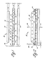
- the improved semiconductor power device 10 in accordance with the present invention is shown in an exploded partial cross-sectional illustration.
- the improved semiconductor device 10 is shown to include a conventional semiconductor device as a substrate member 12 and first and second semiconductor heat sink electrodes 14 and 16, respectively, for attachment to the substrate.
- the conventional semiconductor device 12 can comprise a number of different power devices, for the purposes of illustration, the device 12 has been selected to have a recessed gate structure and can, for instance, be an edge-gated silicon power thyristor which has been fabricated of a silicon wafer.
- the configuration of the device may be more apparent from Figure 3 discussed below.
- the gate electrode can have an involute structure.
- the conventional semiconductor device substrate 12, shown in Figure 1 includes a first lower surface 18 and a second upper surface 20.
- a first terminal 22, such as a substantially planar anode terminal 22 has been fabricated in the first surface 18 of the device 12 and second and third terminals 24 and 25 respectively, have been fabricated in the second surface 20 of the device.
- the second terminal 24 appears as a plurality of mesa cathodes while the third terminal 25 appears as a plurality of recessed gates.
- the cathode terminal 24 is illustrated as an unrecessed region 26 having a substantially planar upper surface 29 and substantially cylindrical interior and exterior walls 30 and 32, respectively.
- the circular shaped cathode and gate terminals 24 and 25 respectively can be considered to circumferentially define each other's boundaries.
- the first and second semiconductor heat sink electrodes 14 and 16 have been fabricated as substantially planar semiconductor wafers having interior surfaces which are intended to join or contact the first and second surfaces 18 and 20, respectively, of the device 12. If the first and second surfaces 18 and 20 of the device 12 are irregular, the corresponding electrode can include the mirror image of the irregularity to provide a mating contact.
- the first semiconductor electrode is typically provided with substantially planar first and second surfaces 50 and 52.
- the first surface 50 is substantially coextensive with the substrate 12 of the device and is specially configured to engage substantially the entire lower surface of the substantially planar first or anode terminal 22 of the device 12.
- the second electrode 16 in the illustrated typical example is also substantially planar and has first and second substantially planar surfaces 56 and 58.
- the first surface 56 is configured to engage substantially the entire surface 29 of the second or cathode terminal 24 of the device 12 disposed on the second surface 20 thereof.
- the second electrode 16 makes electrical contact with only the cathode electrode 24 and does not make electrical contact with the gate electrode 25.
- the second electrode 16 in the illustrated embodiment is less than coextensive with the conventional device 12 and does not cover the entire second surface 20 of the device 12. Immediate and direct access to an exposed portion of the gate electrode 25 disposed about the periphery of the device 12 is provided in the illustrated example.
- the second electrode 16 can be coextensive with the substrate and can, for instance, have a central opening for providing access to the central gate electrode and to allow an appropriate connection to be made thereto.
- portions of the device terminals not covered by an electrode can be sealed with a passivation layer.
- each of the first and second electrodes 14 and 16, respectively be fabricated from degeneratively doped highly electrically conductive semiconductor material having a coefficient of thermal expansion essentially equal to the coefficient of thermal expansion of the substrate containing the conventional device 12. It is also preferred that the electrodes 14 and 16 be fabricated from degenerately doped polycrystalline semiconductor materials such as low cost single crystalline, poly quality, or polycrystalline silicon. In the illustrated embodiment employing a silicon device, the electrodes 14 and 16 are fabricated from silicon wafers. It is also preferred that the first and second electrodes 14 and 16 respectively, have a thickness T2 and T3, each of which is less than the thickness T1 of the device substrate 12 of the conventional device.
- the substrate 12 exhibits a thickness in the range of 30-50 mils, and the first and second electrodes exhibit thicknesses in the range of 20-40 mils.
- the substrate 12 can have a radius of approximately 3 inches or more.
- the improved semiconductor device embodiment described herein can be advantageously implemented as a high power device or a device which, under reverse bias conditions, can block up to several thousand volts, and typically block voltages in the range of 2000-6000 volts.
- first and second electrodes 14 and 16 respectively be permanently attached to the terminal surfaces of the semiconductor power device 12 by, for instance, a hard alloy or eutectic bond. It has been found that an aluminum silicon eutectic bond fixedly attaches the first and second silicon electrodes 14 and 16 respectively, to the first and second surfaces 18 and 20 of the semiconductor device 12 in a manner to avoid slip or creep between the electrode and the substrate of the device 12.
- each surface of the device 12 and electrodes 14 and 16 to be bonded is coated with a thin film or layer of aluminum 60, preferably having a thickness in the range of .1-.5 mils.
- This layer of aluminum can be applied, for instance, by vacuum deposition or sputtering.
- a three layer sandwich comprising the second electrode 16, the device 12, and the first electrode 14 is formed.
- the sandwich is then heated in, for instance, a hydrogen atmosphere for a period of one half an hour at a temperature in the range of 500°C-700°C to establish a eutectic bond between the substrate 12 and electrodes 14 and 16. It is preferred that all bonding be accomplished at temperatures less than 700°C to avoid unwanted impurity diffusions in the semiconductor materials to avoid harm to the device 12.
- the improved device 10 comprises a unitary package having a three layer structure of semiconductor electrode 14, semiconductor device substrate 12 and semiconductor electrode 16 or in the example under consideration, silicon electrode 14, silicon device substrate 12 and silicon electrode 16.
- semiconductor electrodes 14 and 16 in addition to providing low electrical resistance contacts between the device 12 and an external terminal also serve to reduce the thermal stress applied to the device inasmuch as the coefficients of thermal expansion of the electrodes 14 and 16 closely matches the coefficient of thermal expansion of the device 12.
- the electrodes 14 and 16 readily absorb heat from the device 12 and contribute to improved thermal dissipation from the improved device comprising the conventional device 12 encased within the semiconductor electrodes 14 and 16.
- the improved packaged device 12 is better able to withstand heat surges by readily dissipating the generated heat.
- the eutectic bond is an essentially negligible thermal barrier which allows heat from the semiconductor device 12 to readily travel into the electrodes 14 and 16 to a depth of approximately 30 mils in less than 8.3 milliseconds to avoid damage to the device following each half cycle current/power surge in normal 60 Hz operation.
- an additional external heat sink 75 can be applied to either or both the electrodes 14 and 16.
- the additional heat sink 75 is applied only to the second surface 58 of the second electrode 16.
- the more massive heat sink 75 can be fluid cooled.
- External terminals 80, 82, and 88 can be applied respectively to the anode, cathode, and gate terminals of the device 12.
- Epoxy, soft solder, or other low temperature bonding techniques can be used to attach the heat sink 75 or external terminal 80 and 82 to the appropriate electrode 14 or 16 to avoid damage to the previously formed eutectic bond between the electrodes 14 and 16 and the device 12.
- the heat sink 75 and terminal 80 can be attached by high temperature bonding; however, it is preferred that the high temperature bond be accomplished prior to formation of the eutectic bonds between the electrodes 14 and 16 and device substrate 12 to avoid contamination of the device which might otherwise occur by thermally inducing impurities to enter the device 12.
- the massive aluminum or copper heat sinks 75 can be attached to the encased or improved device by a liquid metal interface, for instance, using a gallium layer.
- the electrodes 14 and 16 are permanently bonded to the device 12 and essentially hermetically seal those surfaces of the device 12 which they cover.
- the edge region 85 of the device such as the cathode surface 20 not covered by and projecting past the electrode 16, can also be sealed with a passivation layer 90 to provide a hermetic enclosure for the device.
- the edge region 85 of the device 12 containing a portion of the gate electrode 25 which projects past the electrode 16, can have an external terminal 88 connected thereto and can be covered with appropriate passivation material 90 such as room temperature vulcanizable silicon (RTV) or alternatively, a native semiconductor oxide such as silicon dioxide.
- RTV room temperature vulcanizable silicon
- the passivation material 90 coats and seals all exposed surfaces of the device 12 and the adjacent surface 28 of the electrode.
- the passivation material 90 can coat and seal the cathode surface 20, the gate surface 25 and the adjacent surface 28 of the electrode 16. It is preferred in the illustrated example that passivation layer 90 coat the entire periphery of the cathode 24, the gate 25, and the adjacent edge 28 of the electrode 16 to seal the second surface 20 of the device 12 within the electrode 16.
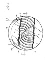
- Figure 3 is a top plan view partially in cut away of the packaging system 10 of the present invention.
- the second electrode 16 is fixedly secured to the second surface 20, shown in Figure 1, of the device substrate 12.
- the device 12 is a thyristor having gate and cathode electrodes 24 and 26, respectively, interlaced in an involute structure on the upper surface 20 of the device 12.
- the edge gate terminal 88 passes through and is sealed within a layer of native oxide 90 such as silicon dioxide.
- the cathode terminal 82 is not shown in Figure 3.
- the first electrode 14 supports the device 12 from beneath.
- the first and second electrodes, in combination with the oxide layer 90, form a hermetically sealed all semiconductor package 10 for the device 12.
- the more massive heat sinks 75 have been omitted from Figure 3.
Landscapes
- Cooling Or The Like Of Semiconductors Or Solid State Devices (AREA)
- Die Bonding (AREA)
- Thyristors (AREA)
Applications Claiming Priority (2)
| Application Number | Priority Date | Filing Date | Title |
|---|---|---|---|
| US80025185A | 1985-11-21 | 1985-11-21 | |
| US800251 | 1985-11-21 |
Publications (2)
| Publication Number | Publication Date |
|---|---|
| EP0224141A2 true EP0224141A2 (fr) | 1987-06-03 |
| EP0224141A3 EP0224141A3 (fr) | 1989-06-14 |
Family
ID=25177894
Family Applications (1)
| Application Number | Title | Priority Date | Filing Date |
|---|---|---|---|
| EP86115795A Withdrawn EP0224141A3 (fr) | 1985-11-21 | 1986-11-13 | Dispositifs de puissance à semi-conducteur |
Country Status (2)
| Country | Link |
|---|---|
| EP (1) | EP0224141A3 (fr) |
| JP (1) | JPS62155564A (fr) |
Cited By (3)
| Publication number | Priority date | Publication date | Assignee | Title |
|---|---|---|---|---|
| EP0266093A3 (en) * | 1986-10-27 | 1988-09-28 | Electric Power Research Institute, Inc | High power multi-layer semiconductive switching device with multiple parallel contacts |
| GB2246471A (en) * | 1988-08-23 | 1992-01-29 | Nobuo Mikoshiba | Cooling semiconductor devices |
| GB2246472A (en) * | 1988-08-23 | 1992-01-29 | Nobuo Mikoshiba | Cooling semiconductor devices |
Families Citing this family (1)
| Publication number | Priority date | Publication date | Assignee | Title |
|---|---|---|---|---|
| JPS62152464U (fr) * | 1986-03-19 | 1987-09-28 |
Family Cites Families (4)
| Publication number | Priority date | Publication date | Assignee | Title |
|---|---|---|---|---|
| FR2378354A1 (fr) * | 1977-01-19 | 1978-08-18 | Alsthom Atlantique | Procede de fabrication de semiconducteurs de puissance a contacts presses |
| JPS603776B2 (ja) * | 1977-06-03 | 1985-01-30 | 株式会社日立製作所 | 半導体素子 |
| US4373255A (en) * | 1979-06-19 | 1983-02-15 | The United States Of America As Represented By The Secretary Of The Air Force | Method of making oxide passivated mesa epitaxial diodes with integral plated heat sink |
| EP0042693B1 (fr) * | 1980-06-21 | 1985-03-27 | LUCAS INDUSTRIES public limited company | Composant de puissance à semi-conducteur et procédé pour sa fabrication |
-
1986
- 1986-11-13 EP EP86115795A patent/EP0224141A3/fr not_active Withdrawn
- 1986-11-20 JP JP61275531A patent/JPS62155564A/ja active Pending
Cited By (4)
| Publication number | Priority date | Publication date | Assignee | Title |
|---|---|---|---|---|
| EP0266093A3 (en) * | 1986-10-27 | 1988-09-28 | Electric Power Research Institute, Inc | High power multi-layer semiconductive switching device with multiple parallel contacts |
| GB2246471A (en) * | 1988-08-23 | 1992-01-29 | Nobuo Mikoshiba | Cooling semiconductor devices |
| GB2246472A (en) * | 1988-08-23 | 1992-01-29 | Nobuo Mikoshiba | Cooling semiconductor devices |
| GB2246471B (en) * | 1988-08-23 | 1993-07-28 | Nobuo Mikoshiba | Cooling semiconductor devices |
Also Published As
| Publication number | Publication date |
|---|---|
| EP0224141A3 (fr) | 1989-06-14 |
| JPS62155564A (ja) | 1987-07-10 |
Similar Documents
| Publication | Publication Date | Title |
|---|---|---|
| US3280389A (en) | Freely expanding pressure mounted semiconductor device | |
| US4249034A (en) | Semiconductor package having strengthening and sealing upper chamber | |
| US6703707B1 (en) | Semiconductor device having radiation structure | |
| US3609471A (en) | Semiconductor device with thermally conductive dielectric barrier | |
| JP2726222B2 (ja) | カットオフ可能な高出力半導体素子 | |
| US4996586A (en) | Crimp-type semiconductor device having non-alloy structure | |
| US3601667A (en) | A semiconductor device with a heat sink having a foot portion | |
| EP0114917A2 (fr) | Empaquetages pour semi-conducteurs | |
| JPH11330283A (ja) | 半導体モジュール及び大型半導体モジュール | |
| US3387191A (en) | Strain relieving transition member for contacting semiconductor devices | |
| CA2139452A1 (fr) | Emballage hermetique destine a un dispositif semiconducteur grande puissance | |
| EP0246539B1 (fr) | Empaquetages en silicium pour des dispositifs de puissance semi-conducteurs | |
| US3742599A (en) | Processes for the fabrication of protected semiconductor devices | |
| US3280384A (en) | Encapsuled semiconductor device with lapped surface connector | |
| CA1157135A (fr) | Thyristor photocommande | |
| EP0224141A2 (fr) | Dispositifs de puissance à semi-conducteur | |
| US4609937A (en) | Power semiconductor device with O-ring seal | |
| US3277957A (en) | Heat transfer apparatus for electronic component | |
| US3581163A (en) | High-current semiconductor rectifier assemblies | |
| EP0788152B1 (fr) | Dispositif semi-conducteur assemblé par compression interne avec un cadre de puce permettant une distance de fuite plus longue | |
| US2917686A (en) | Semiconductor rectifier device | |
| JPS6137784B2 (fr) | ||
| US5585310A (en) | Methods of mass production of semiconductor devices | |
| EP0244767A2 (fr) | Boîtier hermétique pour semi-conducteur et procédé de fabrication | |
| JP7203214B2 (ja) | 浮動性実装を有する電力半導体装置 |
Legal Events
| Date | Code | Title | Description |
|---|---|---|---|
| PUAI | Public reference made under article 153(3) epc to a published international application that has entered the european phase |
Free format text: ORIGINAL CODE: 0009012 |
|
| AK | Designated contracting states |
Kind code of ref document: A2 Designated state(s): CH LI SE |
|
| PUAL | Search report despatched |
Free format text: ORIGINAL CODE: 0009013 |
|
| AK | Designated contracting states |
Kind code of ref document: A3 Designated state(s): CH LI SE |
|
| 17P | Request for examination filed |
Effective date: 19891109 |
|
| STAA | Information on the status of an ep patent application or granted ep patent |
Free format text: STATUS: THE APPLICATION IS DEEMED TO BE WITHDRAWN |
|
| 18D | Application deemed to be withdrawn |
Effective date: 19910601 |
|
| RIN1 | Information on inventor provided before grant (corrected) |
Inventor name: CUSANO, DOMINIC ANTHONY |