EP0224559B1 - Leitungsverbindung für gedruckte schaltungen - Google Patents
Leitungsverbindung für gedruckte schaltungen Download PDFInfo
- Publication number
- EP0224559B1 EP0224559B1 EP86903814A EP86903814A EP0224559B1 EP 0224559 B1 EP0224559 B1 EP 0224559B1 EP 86903814 A EP86903814 A EP 86903814A EP 86903814 A EP86903814 A EP 86903814A EP 0224559 B1 EP0224559 B1 EP 0224559B1
- Authority
- EP
- European Patent Office
- Prior art keywords
- contact
- contact portion
- section
- electrical terminal
- terminal
- Prior art date
- Legal status (The legal status is an assumption and is not a legal conclusion. Google has not performed a legal analysis and makes no representation as to the accuracy of the status listed.)
- Expired
Links
- 238000003780 insertion Methods 0.000 claims description 10
- 230000037431 insertion Effects 0.000 claims description 10
- 239000002184 metal Substances 0.000 claims description 3
- 238000009434 installation Methods 0.000 description 2
- 238000004519 manufacturing process Methods 0.000 description 1
- 239000000463 material Substances 0.000 description 1
Images


Classifications
-
- H—ELECTRICITY
- H01—ELECTRIC ELEMENTS
- H01R—ELECTRICALLY-CONDUCTIVE CONNECTIONS; STRUCTURAL ASSOCIATIONS OF A PLURALITY OF MUTUALLY-INSULATED ELECTRICAL CONNECTING ELEMENTS; COUPLING DEVICES; CURRENT COLLECTORS
- H01R12/00—Structural associations of a plurality of mutually-insulated electrical connecting elements, specially adapted for printed circuits, e.g. printed circuit boards [PCB], flat or ribbon cables, or like generally planar structures, e.g. terminal strips, terminal blocks; Coupling devices specially adapted for printed circuits, flat or ribbon cables, or like generally planar structures; Terminals specially adapted for contact with, or insertion into, printed circuits, flat or ribbon cables, or like generally planar structures
- H01R12/50—Fixed connections
- H01R12/51—Fixed connections for rigid printed circuits or like structures
- H01R12/55—Fixed connections for rigid printed circuits or like structures characterised by the terminals
- H01R12/58—Fixed connections for rigid printed circuits or like structures characterised by the terminals terminals for insertion into holes
- H01R12/585—Terminals having a press fit or a compliant portion and a shank passing through a hole in the printed circuit board
-
- H—ELECTRICITY
- H01—ELECTRIC ELEMENTS
- H01R—ELECTRICALLY-CONDUCTIVE CONNECTIONS; STRUCTURAL ASSOCIATIONS OF A PLURALITY OF MUTUALLY-INSULATED ELECTRICAL CONNECTING ELEMENTS; COUPLING DEVICES; CURRENT COLLECTORS
- H01R13/00—Details of coupling devices of the kinds covered by groups H01R12/70 or H01R24/00 - H01R33/00
- H01R13/02—Contact members
- H01R13/04—Pins or blades for co-operation with sockets
- H01R13/05—Resilient pins or blades
- H01R13/052—Resilient pins or blades co-operating with sockets having a circular transverse section
Definitions
- the present invention relates to an electrical terminal for interconnecting a circuit board with a power supply section, and more particularly to an electrical terminal which occupies minimal space and requires no tools for connection to the circuit board or the power supply.
- Electrical terminals for transmitting current from a power supply section to circuit elements on a circuit board are known in the industry.
- the electrical terminal shown in Figure 1 is one such terminal.
- the power supply is connected to the connector through the use of a screw requiring the use of tools for proper installation. This is particularly labor intensive when the circuit board has a large current capacity which requires a plurality of terminals, each of which must have the power supply individually secured by a screw. Further, this type of design occupies a relatively large area on the circuit board which causes problems when high density circuit elements are required.
- the contact pins cannot be arranged at equal intervals corresponding with the holes of the circuit board because the width of the terminal must be relatively large in order to allow for insertion of the screw and to provide for a flat power supply receiving surface having a width at least equal to the width of the power supply source. Consequently, the rows of contact pins must be spaced from each other more than an optimal amount.
- the press-fit type contact pins used in terminals of this type are disclosed in US Patent No. 4 186 982. It is essential that the material of the contact pin have a thickness sufficient to withstand the large elastic force which is applied thereto. In order for easy manufacture of terminals using this contact pin, the thickness required for the contact pin must be maintained throughout the terminal. This can be done in devices such as the above-described electrical terminal which require hardware for installation. However, if the thick metal plate is bent to form a smaller diameter tubular male contact, eliminating the need for hardware, cracks are created on the tubular surface because of the small radius of curvature of the tubular portion.
- An object of the present invention is to provide a compact electrical terminal having a plurality of press-fit type contact pins at one end thereof and a contact portion engageable with a matable contact at the other end.
- the terminal may be easily manufactured and ensures reliable electrical connection while reducing the area needed by the terminal on the circuit board.
- the contact pins include a mounting portion which is resiliently press-fitted into the holes of the circuit board and fixed therein.
- the contact portion is provided with a noncylindrical contact section having a thickness identical with that of the contact pins.
- the contact portion is also provided with a resilient contact arm stamped and formed from a part of the contact portion. Lances are provided so that the terminals may be enclosed in a housing if necessary.
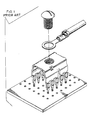
- Figure 2 shows an electrical power terminal 10 of the present invention which is stamped and formed from a metal sheet having desirable conductive and spring characteristics.
- Terminal 10 has a rectangular annular base 11 and a male contact section 18 extending upwardly from base 11.
- Base 11 has a plurality of contact pins 14 which project downward from lower end surfaces of opposed walls 12 and 13. Contact pins 14 are spaced such that pins 14 correspond with the spacing of holes 30 provided on circuit board 50. Although terminal 10 shown in Figure 2 has four contact pins 14, the number of pins 14 varies depending on the current to be transmitted to circuit board 50. The more current transmitted will require more contact pins 14to accommodate the increased current. Contact pins 14 are of the type disclosed in US Patent No. 4 186 982, the disclosure of which is incorporated herein by reference.
- Each contact pin 14 has a mounting portion 15 which is press-fitted in holes 30 of circuit board 50 and fixed therein as discussed below.
- Mounting portion 15 has at least two legs 15a and 15b which have resilient characteristics defining a compliant section. A lateral distance between outside walls of legs 15a, 15b is designed to be greater than the diameter of the holes 30 of circuit board 50.
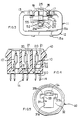
- Male contact section 18 is integral with base 11 end extends upward from an upper end surface of wall portion 13 of base 11.
- Male contact section 18 is comprised of a vertical portion 19 extending from wall portion 13 of base 11, an inclined portion 17 extending from vertical portion 19 and an essentially triangular tip portion 20 extending from inclined portion 17.
- Vertical portion 19 extends in the same plane as wall portion 13.
- Vertical portion 19 has radiussed side edges 19a, as best shown in Figure 3.
- Tip portion 20 extends from inclined portion 17 such that tip portion 20 is parallel to the plane encompassing vertical portion 19.
- a projection 55 is provided on tip portion 20 to allow a female contact section 35 to be easily inserted onto male section 18, as discussed below.
- Tongue 21 is stamped from contact section 18 and extends from a central area of vertical portion 19 to projection 55 on tip portion 20.
- Tongue 21 has a fixed end portion 54 attached to vertical portion 19, a center portion 53 attached to portion 54 and a free end portion 52 attached to portion 53.
- Tongue 21 is bent such that central portion 53 is essentially parallel to vertical portion 19.
- Fixed end portion 54 and free end portion 52 are inclined from central portion 54toward vertical portion 19.
- a contact surface 21 a is provided on central portion 53 and is arcuate to allow female contact section 35 to be easily inserted onto male section 18, as will be discussed.
- Free end portion 52 is provided with laterally projected portions 23 which extend from each side of free end portion 52.
- Lances 24 are provided on either side of vertical portion 19. Lances 24 are attached at one end to vertical section 19, proximate fixed end portion 54 of tongue 21. Opposite ends of lances 24 are curved inward toward wall portion 12 of base 11. A lance 25 is stamped from a section of vertical portion 19 and a section of base 11. Lance 25 is in alignment with tongue 21. A free end of lance 25 extends outward in the opposite direction from that of lances 24.
- Terminal 10 is positioned on circuit board 50 such that holes 30 of circuit board 50 are aligned with contact pins 14. Terminal 10 is then forced downward onto circuit board 50 causing contact pins 14 to engage holes 30. As contact pins 14 are inserted legs 15a, 15b of pins 14 engage wall surfaces of holes 30 causing legs 15a, 15b to be forced inwardly thereby frictionally engaging the wall surfaces of holes 30. This results in terminal 10 being frictionally secured in place on circuit board 50.
- cylindrical female contact section 35 of the power supply is brought into engagement with male contact section 18 of terminal 10.
- Contact section 35 is inserted over tip portion 20 of section 18 such that projection 55 guides female contact section 35 over free end portion 52 of tongue 21.
- an inner wall of section 35 is slid along arcuate contact surface 21 a of tongue 21 and radiussed edges 19a of vertical portion 19. This causes tongue 21 to be biased toward vertical portion 19.
- Projected portions 23 of portion 52 engage inclined portion 17 preventing tongue 21 from further inward movement.
- Radiussed edges 19a and contact surface 21 a enable section 35 to be more easily inserted and also provide an increased contact surface between section 18 and section 35.
- each terminal 10 of the present invention is provided with lances 24 for retaining terminal 10 in housing 40.
- base 11 in order to align contact pins 14 of terminals 10 with holes 30 of circuit board 50 and maintain the required spacing of terminals 10 in housing 40, base 11 must be oriented in different directions as shown by terminals 10 and 10' of Figure 4.
- Housing 40 may have three terminals 10 therein, as shown in Figure 4, or any other number of terminals 10 as is required.
- Eachter- minal 10 is inserted into housing 40 from its lower end into a substantially T-shaped lower bottom opening 31 as shown in Figure 5. As insertion occurs, tongue 21 passes through portion 31 a while the rest of section 18 passes through portion 31 b having a larger width than portion 31 a.
- Lances 24 engage side walls 33 of portion 31 b as insertion occurs, forcing lances 24 to assume a stressed position. Upon full insertion, lances 24 move beyond side walls 33 of portion 31 b allowing lances 24 to return to their original unstressed position in engagement with bottom wall 32. Simultaneously, the upper surface of base 11 engages a recess 60 of a bottom section of housing 40. Lances 25, however, remains in contact with side wall 33a. This positioning of lances 24 and base 11 with respect to bottom wall 32 prevents vertical movement of terminals 10 relative to housing 40.
- a resilient support projection 34 is provided to each opening 31 of bottom wall 32. Each projection 34 engages a back surface of vertical portion 19 of terminal 10. Projections 34 and lances 25 cooperate to prevent horizontal movement of terminals 10 in housing 40.
- FIGS. 6 and 7 show alternative embodiments depicting a male contact 18a and a female contact 18b to be combined with a female contact 35a and a male contact 35b, respectively.
Landscapes
- Coupling Device And Connection With Printed Circuit (AREA)
Claims (11)
Applications Claiming Priority (4)
| Application Number | Priority Date | Filing Date | Title |
|---|---|---|---|
| JP60110632A JPS61271765A (ja) | 1985-05-24 | 1985-05-24 | 電気コネクタ |
| JP110632/85 | 1985-05-24 | ||
| JP8399985U JPH02862Y2 (de) | 1985-06-05 | 1985-06-05 | |
| JP83999/85 | 1985-06-05 |
Publications (2)
| Publication Number | Publication Date |
|---|---|
| EP0224559A1 EP0224559A1 (de) | 1987-06-10 |
| EP0224559B1 true EP0224559B1 (de) | 1989-09-27 |
Family
ID=26425032
Family Applications (1)
| Application Number | Title | Priority Date | Filing Date |
|---|---|---|---|
| EP86903814A Expired EP0224559B1 (de) | 1985-05-24 | 1986-05-14 | Leitungsverbindung für gedruckte schaltungen |
Country Status (3)
| Country | Link |
|---|---|
| EP (1) | EP0224559B1 (de) |
| DE (1) | DE3665964D1 (de) |
| WO (1) | WO1986007201A1 (de) |
Cited By (1)
| Publication number | Priority date | Publication date | Assignee | Title |
|---|---|---|---|---|
| EP4586410A1 (de) * | 2024-01-12 | 2025-07-16 | Honeywell International Inc. | Elektrische anschlussklemme für ein elektronisches gerät |
Families Citing this family (3)
| Publication number | Priority date | Publication date | Assignee | Title |
|---|---|---|---|---|
| FR2763751B1 (fr) * | 1997-05-26 | 2002-11-29 | Proner Comatel Sa | Contact electrique demontable, a pression |
| DE10223382A1 (de) * | 2002-05-25 | 2003-12-04 | Conti Temic Microelectronic | Einpresskontakt |
| DE102008064590B3 (de) * | 2008-12-19 | 2010-07-15 | Tyco Electronics Amp Gmbh | Kontaktanordnung zur Verbindung mit einer polygonalen Buchse |
Family Cites Families (4)
| Publication number | Priority date | Publication date | Assignee | Title |
|---|---|---|---|---|
| FR2028631A5 (de) * | 1969-01-08 | 1970-10-09 | Comp Generale Electricite | |
| US4186982A (en) * | 1973-08-01 | 1980-02-05 | Amp Incorporated | Contact with split portion for engagement with substrate |
| US4219251A (en) * | 1978-12-08 | 1980-08-26 | Litton Systems, Inc. | Power connector |
| JPS57123669A (en) * | 1980-12-15 | 1982-08-02 | Amp Inc | Power distribution block |
-
1986
- 1986-05-14 DE DE8686903814T patent/DE3665964D1/de not_active Expired
- 1986-05-14 EP EP86903814A patent/EP0224559B1/de not_active Expired
- 1986-05-14 WO PCT/US1986/001045 patent/WO1986007201A1/en not_active Ceased
Cited By (1)
| Publication number | Priority date | Publication date | Assignee | Title |
|---|---|---|---|---|
| EP4586410A1 (de) * | 2024-01-12 | 2025-07-16 | Honeywell International Inc. | Elektrische anschlussklemme für ein elektronisches gerät |
Also Published As
| Publication number | Publication date |
|---|---|
| DE3665964D1 (en) | 1989-11-02 |
| EP0224559A1 (de) | 1987-06-10 |
| WO1986007201A1 (en) | 1986-12-04 |
Similar Documents
| Publication | Publication Date | Title |
|---|---|---|
| US4790764A (en) | Electrical power terminal for circuit boards | |
| EP0475067B1 (de) | Elektrischer Steckverbinder und Endstück dafür | |
| US5498167A (en) | Board to board electrical connectors | |
| EP0650230B1 (de) | Sperrmittel für elektrischen Steckverbinder | |
| JP2685287B2 (ja) | 多接点組立体および可撓接点部材 | |
| US6884089B2 (en) | Electrical connector with fixity members having similar shapes as contacts from which contact portions are omitted | |
| EP1147577B1 (de) | Elektrischer flachbauverbinder | |
| JPH03155072A (ja) | ソケットコンタクト | |
| WO1989004592A1 (en) | Chip carrier sockets having improved contact terminals | |
| EP0158413A2 (de) | Elektrischer Stecker mit geringer notwendiger Einsteckkraft und mit beanspruchungsüberwachten Kontakten | |
| WO1985005006A1 (en) | Dual in-line package carrier assembly | |
| US5076804A (en) | Electrical connector assembly for mounting on a printed circuit board | |
| EP0191539A2 (de) | Elektrisches Anschlussendstück für Steckverbinder | |
| EP0140473B1 (de) | Lötfreier elektrischer Leiter für gedruckte Schaltungen und Steckvorrichtung, die diesen verwendet | |
| US20020081870A1 (en) | Electrical connector | |
| US5692920A (en) | Zero insertion force electrical connector and terminal | |
| EP0142311B1 (de) | Elektrische Flachbauverbindergruppe | |
| US5112231A (en) | Electrical card edge connector assembly | |
| EP0400378B1 (de) | Leiterplattensockel mit Kleeblattkontakt | |
| US4509813A (en) | Retaining clip for holding a connector to a panel | |
| NZ202553A (en) | Socket interfacing chip carrier with p.c.b. | |
| EP0224559B1 (de) | Leitungsverbindung für gedruckte schaltungen | |
| CA1075788A (en) | Printed circuit board edge connector | |
| KR900008278B1 (ko) | 전기 리셉터클 | |
| US4968259A (en) | High density chip carrier socket |
Legal Events
| Date | Code | Title | Description |
|---|---|---|---|
| PUAI | Public reference made under article 153(3) epc to a published international application that has entered the european phase |
Free format text: ORIGINAL CODE: 0009012 |
|
| 17P | Request for examination filed |
Effective date: 19870119 |
|
| AK | Designated contracting states |
Kind code of ref document: A1 Designated state(s): DE FR GB IT NL |
|
| 17Q | First examination report despatched |
Effective date: 19881028 |
|
| ITF | It: translation for a ep patent filed | ||
| RAP1 | Party data changed (applicant data changed or rights of an application transferred) |
Owner name: AMP INCORPORATED |
|
| GRAA | (expected) grant |
Free format text: ORIGINAL CODE: 0009210 |
|
| AK | Designated contracting states |
Kind code of ref document: B1 Designated state(s): DE FR GB IT NL |
|
| REF | Corresponds to: |
Ref document number: 3665964 Country of ref document: DE Date of ref document: 19891102 |
|
| RAP2 | Party data changed (patent owner data changed or rights of a patent transferred) |
Owner name: AMP INCORPORATED |
|
| ET | Fr: translation filed | ||
| NLT2 | Nl: modifications (of names), taken from the european patent patent bulletin |
Owner name: AMP INCORPORATED TE HARRISBURG, PENNSYLVANIE, VER. |
|
| PLBE | No opposition filed within time limit |
Free format text: ORIGINAL CODE: 0009261 |
|
| STAA | Information on the status of an ep patent application or granted ep patent |
Free format text: STATUS: NO OPPOSITION FILED WITHIN TIME LIMIT |
|
| 26N | No opposition filed | ||
| ITTA | It: last paid annual fee | ||
| REG | Reference to a national code |
Ref country code: GB Ref legal event code: 732E |
|
| PGFP | Annual fee paid to national office [announced via postgrant information from national office to epo] |
Ref country code: NL Payment date: 19990322 Year of fee payment: 14 |
|
| PGFP | Annual fee paid to national office [announced via postgrant information from national office to epo] |
Ref country code: GB Payment date: 19990406 Year of fee payment: 14 |
|
| PGFP | Annual fee paid to national office [announced via postgrant information from national office to epo] |
Ref country code: FR Payment date: 19990504 Year of fee payment: 14 |
|
| PGFP | Annual fee paid to national office [announced via postgrant information from national office to epo] |
Ref country code: DE Payment date: 19990531 Year of fee payment: 14 |
|
| PG25 | Lapsed in a contracting state [announced via postgrant information from national office to epo] |
Ref country code: GB Free format text: LAPSE BECAUSE OF NON-PAYMENT OF DUE FEES Effective date: 20000514 |
|
| PG25 | Lapsed in a contracting state [announced via postgrant information from national office to epo] |
Ref country code: NL Free format text: LAPSE BECAUSE OF NON-PAYMENT OF DUE FEES Effective date: 20001201 |
|
| GBPC | Gb: european patent ceased through non-payment of renewal fee |
Effective date: 20000514 |
|
| PG25 | Lapsed in a contracting state [announced via postgrant information from national office to epo] |
Ref country code: FR Free format text: LAPSE BECAUSE OF NON-PAYMENT OF DUE FEES Effective date: 20010131 |
|
| NLV4 | Nl: lapsed or anulled due to non-payment of the annual fee |
Effective date: 20001201 |
|
| PG25 | Lapsed in a contracting state [announced via postgrant information from national office to epo] |
Ref country code: DE Free format text: LAPSE BECAUSE OF NON-PAYMENT OF DUE FEES Effective date: 20010301 |
|
| REG | Reference to a national code |
Ref country code: FR Ref legal event code: ST |
|
| PG25 | Lapsed in a contracting state [announced via postgrant information from national office to epo] |
Ref country code: IT Free format text: LAPSE BECAUSE OF NON-PAYMENT OF DUE FEES;WARNING: LAPSES OF ITALIAN PATENTS WITH EFFECTIVE DATE BEFORE 2007 MAY HAVE OCCURRED AT ANY TIME BEFORE 2007. THE CORRECT EFFECTIVE DATE MAY BE DIFFERENT FROM THE ONE RECORDED. Effective date: 20050514 |