EP0224691A2 - Speicheranordnung mit mehrfachem Lese-Schreibzugriff - Google Patents
Speicheranordnung mit mehrfachem Lese-Schreibzugriff Download PDFInfo
- Publication number
- EP0224691A2 EP0224691A2 EP86114207A EP86114207A EP0224691A2 EP 0224691 A2 EP0224691 A2 EP 0224691A2 EP 86114207 A EP86114207 A EP 86114207A EP 86114207 A EP86114207 A EP 86114207A EP 0224691 A2 EP0224691 A2 EP 0224691A2
- Authority
- EP
- European Patent Office
- Prior art keywords
- address
- group
- pointer
- storage unit
- read
- Prior art date
- Legal status (The legal status is an assumption and is not a legal conclusion. Google has not performed a legal analysis and makes no representation as to the accuracy of the status listed.)
- Granted
Links
Images


Classifications
-
- G—PHYSICS
- G06—COMPUTING OR CALCULATING; COUNTING
- G06F—ELECTRIC DIGITAL DATA PROCESSING
- G06F9/00—Arrangements for program control, e.g. control units
- G06F9/06—Arrangements for program control, e.g. control units using stored programs, i.e. using an internal store of processing equipment to receive or retain programs
- G06F9/30—Arrangements for executing machine instructions, e.g. instruction decode
- G06F9/30098—Register arrangements
- G06F9/3012—Organisation of register space, e.g. banked or distributed register file
-
- G—PHYSICS
- G06—COMPUTING OR CALCULATING; COUNTING
- G06F—ELECTRIC DIGITAL DATA PROCESSING
- G06F15/00—Digital computers in general; Data processing equipment in general
- G06F15/76—Architectures of general purpose stored program computers
- G06F15/80—Architectures of general purpose stored program computers comprising an array of processing units with common control, e.g. single instruction multiple data processors
- G06F15/8053—Vector processors
-
- G—PHYSICS
- G06—COMPUTING OR CALCULATING; COUNTING
- G06F—ELECTRIC DIGITAL DATA PROCESSING
- G06F9/00—Arrangements for program control, e.g. control units
- G06F9/06—Arrangements for program control, e.g. control units using stored programs, i.e. using an internal store of processing equipment to receive or retain programs
- G06F9/30—Arrangements for executing machine instructions, e.g. instruction decode
- G06F9/34—Addressing or accessing the instruction operand or the result ; Formation of operand address; Addressing modes
- G06F9/345—Addressing or accessing the instruction operand or the result ; Formation of operand address; Addressing modes of multiple operands or results
Definitions
- the present invention relates to memory systems that read and write data to and from several addresses within a given instruction cycle.
- the memory has to provide for reading and writing data to the memory at a bandwidth which matches the bandwidth of processing.
- One approach for matching the processing bandwidth in the prior art has been the use of the cache concept, that is using a fast memory to contain a working set of data so that the processor has quick access to currently active data.
- the CRAY 1 uses 8 vector registers, each of 64 words, for a total of 512 floating point words, and every vector is used from the beginning and runs consecutively. Thus the CRAY 1 is constrained to a relatively small memory and a rigid addressing scheme.
- One prior art approach to reducing the amount of time required for three memory operations per cycle uses the replicated memory approach. If a single conventional memory bank is used for the three address computation, the memory bank would have to perform two fetches and one store for a total of three units gainful work per cycle.
- the replicated memory approach supplies two identical memory units, and stores everything in duplicate, one copy in each bank, to alleviate the fetch bandwidth. By storing everything in duplicate, the fetch bandwidth is alleviated by fetching one operand from each bank in parallel and storing the result back to both units in parallel.
- Each bank in such a system performs two units of work, one fetch and one store in each cycle, rather than three.
- the replicated memory approach of the prior art appears to be 1.5 times as fast as the single bank memory. So the replicated memory approach of the prior art requires that an instruction cycle squeeze two memory access cycles in, rather than three of the single bank memory.
- Both the single bank memory and the replicated memory approach of the prior art are limited in performance because of the possibility of conflict of accesses to the memory between a read operation and a write operation. Thus the read operation must be done at a time apart from the write operation.
- the present invention provides a memory system to accommodate r read accesses and w write accesses in a memory cycle and comprising r groups of w + 1 independently addressable storage units, each storage unit being addressable by the same spectrum of addresses and each group having a pointer arrangement indicating not more than one storage unit in the group for each address of the spectrum of addresses, by the which it is accessed, together with w + 1 address inputs, a data output and w data inputs, means to connect a different one of the read addresses to each group together with all the write addresses, means to selectively connect the read address connected to a group to that storage unit of the group indicated by the pointer for that address and to selectively connect each data input to a different one of the other storage units, means to connect the read storage unit to the data output and means to change the pointers for the group so as to point at the storage unit of the group connected to the
- the pointer means directs memory accessing to prevent conflicts. Conflicts are always avoided, absent external errors such as two identical addresses in a single presented instruction, which is not expected in this context, because one unit in each of the r groups is directed to supply data in response to a read address and the w remaining units are available for writing data in response to the w write addresses redundantly so that each of the groups of memory units will have valid data in at least one of its w + 1 memory units for a given address.
- the present invention provides a memory system to accommodate two read accesses and one write access in a memory cycle and comprising two groups of two independently addressable storage units, each storage unit being addressable by the same spectrum of addresses and each group having a pointer arrangement indicating not more than one storage unit in the group for each address of the spectrum of addresses, by the which it is accessed, together with an input for one of the read addresses and the write address, a data output and a data input, means to selectively connect the read address connected to a group to that storage unit of the group indicated by the pointer for that address and to selectively connect the data input to the other storage unit, means to connect the read storage unit to the data output and means to set the pointer for the write address to point to the storage unit of the group used for the writing operation.
- a pipelined multiport RAM random access memory
- M locations for storage of data items of width d and which is capable of performing within one cycle r read operations and w write operations, and which has a cycle time t.
- Data items are stored in r groups of units of conventional RAM, which have a cycle time t.
- Each group has w + units, called unit 0,..., unit w of that group.
- Each unit has M locations for storage of data items of width d.
- Each group also has a pointer RAM having a cycle time equal to or less than t/(w + 1).
- the pointer RAM has M locations for storage of data items of width of at least (log 2 (w+ 1 )), so that in one location of the pointer RAM of a group of units one can store a pointer to a particular unit of that group.
- group 0 there are 2 groups of units, say group 0 and group 1.
- Each group has 2 units, called unit 0 and unit 1.
- the pointer RAM for group 0 is called P0 and the pointer RAM for group 1 is calJed P1.
- locations 5, 6, 7 and 8 of the multiport RAM are the values 50, 60, 70 and 80. Further assume that initially locations 5, 6, 7, 8 of unit 0 of each group have valid data, and that this is reflected by value 0 at locations 5, 6, 7, 8 of the two pointer RAMs P0, P1.
- the index b(0,5) of the unit in group 0 which has valid data in location 5 is fetched by a read from location 5 in pointer RAM PO.
- the index b(0,7) of the unit in group 0 which has valid data in location 7 is fetched by a read from location 7 in pointer RAM P0.
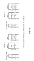
- the memory system is responsive to a first address a(0), a second address a(1) and a third address c(0) within an instruction cycle to supply data read from the first and second addresses and for writing data received to the third address.
- the first, second and third addresses are supplied to address registers 101, 102 and 103 respectively.
- the data read from the first and second addresses is supplied at output registers 129 and 149 respectively.
- the data received for writing to the third address is received in register 133.
- the system 10 includes a first group 11, labelled group 0 of two memory units 126,132, labelled unit 0 and unit 1, respectively.
- the first group 11 is responsive to the first address a(0) from register 101 which is moved through register 121 and multiplexers 124 and 130 to one of the two units 126, 132. Also the first group 11 is responsive to the third address c(0) which is moved through register 123 and through the multiplexers 124 and 130 to the other of the two units, 126, 132.
- Data from the first address a(0) is supplied from one unit of the two units 126, 132 at the respective data output ports 127, 135. Through multiplexer 128 the data is then supplied to the output register 129.
- the data received at the input register 133 is supplied through the drivers 136 or 134 to the data ports 127, 135 of the two units 126,132, only-one of which is enabled for a write.
- the third address c(0) is supplied to that one unit which is enabled for a write and the data is written.
- data is read from one of the two units while data is written to the other of the two units during a given memory access cycle.
- the system further comprises a second group 12, labelled group 1, of two memory units 146, 152 designated unit 0 and unit 1 respectively.
- the second group 12 of two memory units 146, 152 is configured in the same manner as the first group 11, group 0.
- the second address a(1) which is moved through register 122 is supplied to multiplexers 144, 150 in conjunction with the third address c(0) from the register 123.
- the second group supplies data read from one of the two units through the data port 147, 155 and the multiplexer 148 to the output register 149.
- the other unit writes data received from register 133 through the drivers 156 or 154 at the third address c(0).
- a pointer means for controlling the first group 11 and the second group 12 so that the one of the two units containing valid data is read in response to the read address a(0) or a(1) and that data received through register 133 is written to the other unit.
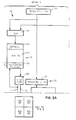
- the pointer means includes means 13, 14 for storing pointers to the units containing valid data at the first and second addresses in the first and second groups, respectively.
- the means 13 is responsive to the first address a(0) from register 101 through multiplexer 104 to provide a pointer at a data output register 108.
- the pointer is stored in the RAM 107 and accessed through address port 106.
- the means 13 is responsive to the third address c(0) in register 103 through multiplexer 104 for writing data received at the data input port 112 to the RAM 107 at the address in the port 106.
- the means 14 associated with the second group 12 includes a similar system except that it is responsive to the second address a(1) from register 102 rather than the first address.
- the pointer means for the first group 11 includes flip-flop 109 which latches the pointer supplied at the data output port 108 of the pointer RAMs 107 corresponding to the first address a(0).
- the pointer is maintained in the flip-flop 109 which provides a true output 110 and a complement output 111.
- the true output 110 and complement output 111 are provided to the first group so that the multiplexers 124 and 130 supply the first address to the one unit having valid data while the other unit is enabled for a write operation.
- the complement output 111 is supplied at the data input port 112 of the pointer RAM 107 so that a pointer indicating that valid data at the third address c(0) is stored in the other unit is written to the pointer RAM 107.
- the second group also includes a second means 16 for supplying the second address a(1) to the one unit in the second group 12 containing valid data and the third address to the other unit in the second group 12. It is configured in the same manner as described above for the first group.
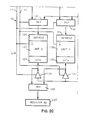
- Read addresses a(0) and a(1) are loaded into registers 101 and 102.
- the write address c(0) is loaded into register 103.
- the pointer value b(0,a(0)) is fetched by routing address a(0) from register 101 via multiplexer 104 to address port 106 of the pointer RAM 107 of unit 0.
- RAM 107 performs a read and the result is loaded from data output port 108 of pointer RAM 107 into flip-flop 109.
- the non-inverting output 110 of flip-flop 109 gives the index of the unit of group 0 that will perform the read operation.
- the inverting output 111 of flip-flop 109 gives the index of the unit of group 0 that will perform the write operation and the new value of b-(O,c(0)) which is routed to the data input port 112 of RAM 107.
- the new pointer value b(O,c(O)) is stored into RAM 107 by routing address c(0) from register 103 via MUX 104 to address port 106 of the pointer RAM 107 of unit 0 and having pointer RAM 107 perform a read operation.
- the pointer value b(1,a(1)) is fetched by routing address a(1) from register 102 via multiplexer 113 to address port 114 of the pointer RAM 115 of unit 1.
- RAM 115 performs a read and the result is loaded from data output port 116 of pointer RAM 115 into flip-flop 117.
- the non-inverting output 118 of flip-flop 117 gives the index of the unit of group 1, which will perform the read operation.
- the inverting output 119 of flip-flop 117 gives the index of the unit of group 1 that will perform the write operation and the new value of b(1,c(0)) which is routed to the data input port 120 of RAM 115.
- the new pointer value b(1,c(0)) is stored into RAM 115 by routing address c(0) from register 103 via MUX 113 to address port 114 of the pointer RAM 115 of unit 1 and having pointer RAM 115 perform a read operation.
- the select lines of multiplexers 124, 130 and 128, the (active low) write signals of memory units 126 and 132 as well as the (active low) output enable signals of drivers 134 and 136 are directly controlled by the non-inverted output 110 and the inverted output 111 of flip-flop 109.
- the pipelined read address a'(1) in register 122 is routed via MUX 144 to address port 145 of memory unit 146 which is unit 0 of group 1.
- Memory unit 146 performs a read operation. The result is routed from the data port 147 of memory unit 146 via MUX 148 to the data output register 149 of group 1.
- the pipelined write address c'(0) in register 123 is routed via MUX 150 to address port 151 of memory unit 152, which is unit 1 of group 1.
- the data to be written into the multiport RAM is routed from data input register 133 via driver 154 to the data port 155 of memory unit 152.
- Memory unit 152 performs a write operation.
- the select lines of multiplexers 144, 150 and 148, the (active low) write signals of memory units 146 and 152 as well as the (active low) output enable signals of drivers 154 and 156 are directly controlled by the non-inverted output 118 and the inverted output 119 of flip-flop 117.
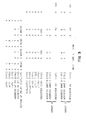
- FIG. 3 shows a self explanatory timing diagram for the system of FIGS. 2A, 2B, 2C and 2D when the operations illustrated in FIGS. 1 A, 1 B and 1C are executed.
- Table 1 gives a list of widely available components which can be used to build the system of FIG. 2. Using these components a 3-port RAM with 2K memory locations, a cycle time of about 100 ns and capable of performing 2 reads and 1 write in 1 cycle can be built. This matches the 100 ns cycle time of the fastest floating point ALU and multiplier chips presently available.
- the pointer RAMs can be made to operate very quickly, and the action of the pointer RAMs can be made to overlap in time with the operation of the memory units. Thereby, the system performs the work of the multiple reads and writes in essentially the cycle time of the memory units providing a significant performance advantage over the prior art.
Landscapes
- Engineering & Computer Science (AREA)
- Theoretical Computer Science (AREA)
- Software Systems (AREA)
- Physics & Mathematics (AREA)
- General Engineering & Computer Science (AREA)
- General Physics & Mathematics (AREA)
- Computer Hardware Design (AREA)
- Computing Systems (AREA)
- Static Random-Access Memory (AREA)
- Complex Calculations (AREA)
Applications Claiming Priority (4)
| Application Number | Priority Date | Filing Date | Title |
|---|---|---|---|
| US80420685A | 1985-12-02 | 1985-12-02 | |
| US804206 | 1985-12-02 | ||
| US811624 | 1985-12-20 | ||
| US06/811,624 US4766535A (en) | 1985-12-20 | 1985-12-20 | High-performance multiple port memory |
Publications (3)
| Publication Number | Publication Date |
|---|---|
| EP0224691A2 true EP0224691A2 (de) | 1987-06-10 |
| EP0224691A3 EP0224691A3 (en) | 1989-12-20 |
| EP0224691B1 EP0224691B1 (de) | 1993-02-10 |
Family
ID=27122674
Family Applications (1)
| Application Number | Title | Priority Date | Filing Date |
|---|---|---|---|
| EP19860114207 Expired - Lifetime EP0224691B1 (de) | 1985-12-02 | 1986-10-14 | Speicheranordnung mit mehrfachem Lese-Schreibzugriff |
Country Status (2)
| Country | Link |
|---|---|
| EP (1) | EP0224691B1 (de) |
| DE (1) | DE3687739T2 (de) |
Cited By (5)
| Publication number | Priority date | Publication date | Assignee | Title |
|---|---|---|---|---|
| GB2216307A (en) * | 1988-03-01 | 1989-10-04 | Ardent Computer Corp | Vector register file |
| GB2332539A (en) * | 1997-12-17 | 1999-06-23 | Fujitsu Ltd | Accessing random access memories |
| GB2369215A (en) * | 2000-10-25 | 2002-05-22 | Samsung Electronics Co Ltd | Memory device and Reed Solomon decoder including the memory device |
| WO2005010748A1 (en) * | 2003-07-30 | 2005-02-03 | Koninklijke Philips Electronics, N.V. | Memory organization allowing single cycle pointer addressing where the address of the pointer is also contained in one of the memory locations |
| CN119645321A (zh) * | 2025-02-19 | 2025-03-18 | 广州壁仞集成电路有限公司 | 数据读取方法、装置、电子设备和计算机可读存储介质 |
Family Cites Families (3)
| Publication number | Priority date | Publication date | Assignee | Title |
|---|---|---|---|---|
| US3737866A (en) * | 1971-07-27 | 1973-06-05 | Data General Corp | Data storage and retrieval system |
| US4456965A (en) * | 1980-10-14 | 1984-06-26 | Texas Instruments Incorporated | Data processing system having multiple buses |
| JPS59213084A (ja) * | 1983-05-16 | 1984-12-01 | Fujitsu Ltd | バッファ記憶装置のアクセス制御方式 |
-
1986
- 1986-10-14 DE DE19863687739 patent/DE3687739T2/de not_active Expired - Fee Related
- 1986-10-14 EP EP19860114207 patent/EP0224691B1/de not_active Expired - Lifetime
Cited By (14)
| Publication number | Priority date | Publication date | Assignee | Title |
|---|---|---|---|---|
| GB2216307B (en) * | 1988-03-01 | 1992-08-26 | Ardent Computer Corp | Vector register file |
| GB2216307A (en) * | 1988-03-01 | 1989-10-04 | Ardent Computer Corp | Vector register file |
| GB2332539B (en) * | 1997-12-17 | 2003-04-23 | Fujitsu Ltd | Memory access methods and devices for use with random access memories |
| GB2332539A (en) * | 1997-12-17 | 1999-06-23 | Fujitsu Ltd | Accessing random access memories |
| US6418077B1 (en) | 1997-12-17 | 2002-07-09 | Fujitsu Limited | Memory access methods and devices for use with random access memories |
| GB2381103B (en) * | 1997-12-17 | 2003-06-04 | Fujitsu Ltd | Memory access methods and devices for use with random access memories |
| US6556506B2 (en) | 1997-12-17 | 2003-04-29 | Fujitsu Limited | Memory access methods and devices for use with random access memories |
| GB2381103A (en) * | 1997-12-17 | 2003-04-23 | Fujitsu Ltd | Memory access methods and devices for use with random access memories |
| GB2369215A (en) * | 2000-10-25 | 2002-05-22 | Samsung Electronics Co Ltd | Memory device and Reed Solomon decoder including the memory device |
| GB2369215B (en) * | 2000-10-25 | 2003-04-16 | Samsung Electronics Co Ltd | Memory device, method of accessing the memory device, and reed-solomon decoder including the memory device |
| KR100370239B1 (ko) * | 2000-10-25 | 2003-01-29 | 삼성전자 주식회사 | 고속 블럭 파이프라인 구조의 리드-솔로몬 디코더에적용하기 위한 메모리 장치와 메모리 액세스 방법 및 그메모리 장치를 구비한 리드-솔로몬 디코더 |
| US6639865B2 (en) | 2000-10-25 | 2003-10-28 | Samsung Electronics Co., Ltd. | Memory device, method of accessing the memory device, and reed-solomon decoder including the memory device |
| WO2005010748A1 (en) * | 2003-07-30 | 2005-02-03 | Koninklijke Philips Electronics, N.V. | Memory organization allowing single cycle pointer addressing where the address of the pointer is also contained in one of the memory locations |
| CN119645321A (zh) * | 2025-02-19 | 2025-03-18 | 广州壁仞集成电路有限公司 | 数据读取方法、装置、电子设备和计算机可读存储介质 |
Also Published As
| Publication number | Publication date |
|---|---|
| DE3687739T2 (de) | 1993-08-19 |
| EP0224691A3 (en) | 1989-12-20 |
| EP0224691B1 (de) | 1993-02-10 |
| DE3687739D1 (de) | 1993-03-25 |
Similar Documents
| Publication | Publication Date | Title |
|---|---|---|
| US4766535A (en) | High-performance multiple port memory | |
| US4722049A (en) | Apparatus for out-of-order program execution | |
| EP1047989B1 (de) | Digitaler signalprozessor mit datenausrichtungspuffer für nichtausgerichtete datenzugriffe | |
| US6668316B1 (en) | Method and apparatus for conflict-free execution of integer and floating-point operations with a common register file | |
| US5848432A (en) | Data processor with variable types of cache memories | |
| US5832290A (en) | Apparatus, systems and method for improving memory bandwidth utilization in vector processing systems | |
| US4980817A (en) | Vector register system for executing plural read/write commands concurrently and independently routing data to plural read/write ports | |
| US4325116A (en) | Parallel storage access by multiprocessors | |
| US4339804A (en) | Memory system wherein individual bits may be updated | |
| US5239642A (en) | Data processor with shared control and drive circuitry for both breakpoint and content addressable storage devices | |
| US4725973A (en) | Vector processor | |
| US5974533A (en) | Data processor | |
| US5440717A (en) | Computer pipeline including dual-ported, content-addressable writebuffer | |
| KR970011208B1 (ko) | 파이프라인된 기록버퍼 레지스터 | |
| JPH06242955A (ja) | スーパースカラ・プロセッサ・システムにおける中間記憶バッファの割当てをインデックスする方法およびシステム | |
| JPH06242954A (ja) | 独立にアクセスされる中間記憶域を利用してスーパースカラ・プロセッサ・システムにおける命令ディスパッチを改善する方法およびシステム | |
| JP3641031B2 (ja) | 命令装置 | |
| US5168573A (en) | Memory device for storing vector registers | |
| US4761754A (en) | Vector processor wherein outputs of vector registers are fixedly coupled to inputs of vector calculators | |
| US5420997A (en) | Memory having concurrent read and writing from different addresses | |
| EP0224691B1 (de) | Speicheranordnung mit mehrfachem Lese-Schreibzugriff | |
| JPH0282330A (ja) | ムーブアウト・システム | |
| JPS63501904A (ja) | 統合したマルチコンピュ−タデ−タ処理装置 | |
| JPH02242429A (ja) | パイプライン浮動小数点ロード・インストラクシヨン回路 | |
| US4348723A (en) | Control store test selection logic for a data processing system |
Legal Events
| Date | Code | Title | Description |
|---|---|---|---|
| PUAI | Public reference made under article 153(3) epc to a published international application that has entered the european phase |
Free format text: ORIGINAL CODE: 0009012 |
|
| AK | Designated contracting states |
Kind code of ref document: A2 Designated state(s): DE FR GB IT |
|
| 17P | Request for examination filed |
Effective date: 19871023 |
|
| PUAL | Search report despatched |
Free format text: ORIGINAL CODE: 0009013 |
|
| RHK1 | Main classification (correction) |
Ipc: G06F 13/16 |
|
| AK | Designated contracting states |
Kind code of ref document: A3 Designated state(s): DE FR GB IT |
|
| 17Q | First examination report despatched |
Effective date: 19911022 |
|
| GRAA | (expected) grant |
Free format text: ORIGINAL CODE: 0009210 |
|
| AK | Designated contracting states |
Kind code of ref document: B1 Designated state(s): DE FR GB IT |
|
| PG25 | Lapsed in a contracting state [announced via postgrant information from national office to epo] |
Ref country code: IT Free format text: LAPSE BECAUSE OF FAILURE TO SUBMIT A TRANSLATION OF THE DESCRIPTION OR TO PAY THE FEE WITHIN THE PRESCRIBED TIME-LIMIT;WARNING: LAPSES OF ITALIAN PATENTS WITH EFFECTIVE DATE BEFORE 2007 MAY HAVE OCCURRED AT ANY TIME BEFORE 2007. THE CORRECT EFFECTIVE DATE MAY BE DIFFERENT FROM THE ONE RECORDED. Effective date: 19930210 |
|
| REF | Corresponds to: |
Ref document number: 3687739 Country of ref document: DE Date of ref document: 19930325 |
|
| ET | Fr: translation filed | ||
| PLBE | No opposition filed within time limit |
Free format text: ORIGINAL CODE: 0009261 |
|
| STAA | Information on the status of an ep patent application or granted ep patent |
Free format text: STATUS: NO OPPOSITION FILED WITHIN TIME LIMIT |
|
| 26N | No opposition filed | ||
| PGFP | Annual fee paid to national office [announced via postgrant information from national office to epo] |
Ref country code: GB Payment date: 19950926 Year of fee payment: 10 |
|
| PGFP | Annual fee paid to national office [announced via postgrant information from national office to epo] |
Ref country code: FR Payment date: 19951009 Year of fee payment: 10 |
|
| PGFP | Annual fee paid to national office [announced via postgrant information from national office to epo] |
Ref country code: DE Payment date: 19951030 Year of fee payment: 10 |
|
| PG25 | Lapsed in a contracting state [announced via postgrant information from national office to epo] |
Ref country code: GB Effective date: 19961014 |
|
| GBPC | Gb: european patent ceased through non-payment of renewal fee |
Effective date: 19961014 |
|
| PG25 | Lapsed in a contracting state [announced via postgrant information from national office to epo] |
Ref country code: FR Effective date: 19970630 |
|
| PG25 | Lapsed in a contracting state [announced via postgrant information from national office to epo] |
Ref country code: DE Effective date: 19970701 |
|
| REG | Reference to a national code |
Ref country code: FR Ref legal event code: ST |