EP0225512B1 - Circuit de synchronisation d'horloge numérique librement oscillante - Google Patents
Circuit de synchronisation d'horloge numérique librement oscillante Download PDFInfo
- Publication number
- EP0225512B1 EP0225512B1 EP86115966A EP86115966A EP0225512B1 EP 0225512 B1 EP0225512 B1 EP 0225512B1 EP 86115966 A EP86115966 A EP 86115966A EP 86115966 A EP86115966 A EP 86115966A EP 0225512 B1 EP0225512 B1 EP 0225512B1
- Authority
- EP
- European Patent Office
- Prior art keywords
- signal
- output
- input
- delay
- logic element
- Prior art date
- Legal status (The legal status is an assumption and is not a legal conclusion. Google has not performed a legal analysis and makes no representation as to the accuracy of the status listed.)
- Expired
Links
- 230000007704 transition Effects 0.000 claims description 7
- 230000000295 complement effect Effects 0.000 claims 1
- 230000001172 regenerating effect Effects 0.000 claims 1
- 238000010586 diagram Methods 0.000 description 4
- 230000001360 synchronised effect Effects 0.000 description 4
- 230000001934 delay Effects 0.000 description 2
- 230000000630 rising effect Effects 0.000 description 2
- 230000002411 adverse Effects 0.000 description 1
- 238000010276 construction Methods 0.000 description 1
- 238000000034 method Methods 0.000 description 1
- 230000008520 organization Effects 0.000 description 1
- 239000004065 semiconductor Substances 0.000 description 1
Images

Classifications
-
- H—ELECTRICITY
- H03—ELECTRONIC CIRCUITRY
- H03K—PULSE TECHNIQUE
- H03K3/00—Circuits for generating electric pulses; Monostable, bistable or multistable circuits
- H03K3/02—Generators characterised by the type of circuit or by the means used for producing pulses
- H03K3/027—Generators characterised by the type of circuit or by the means used for producing pulses by the use of logic circuits, with internal or external positive feedback
- H03K3/03—Astable circuits
Definitions
- the invention relates to an oscillator circuit as mentioned in the preamble of patent claim 1 which is already known from ELECTRONIC No. 12 (1978) pages 82/84:
- Computer systems are required to work efficiently with data stores of different speeds within the same system. If a semiconductor data store is used, the characteristics of the dynamic storage devices require that data in the storage elements be refreshed periodically. If store refresh operations are accomplished internally of the data store, the response time of the store will vary, and, accordingly, fully synchronous operation of a data store and the system central processor is not practical or desirable. Nevertheless, data transfer between the two units must be synchronized.
- One means of effecting synchronization between asynchronously operating units of a computer system involves resynchronization or restarting of a clock signal source of one unit, for example a free-running oscillator forming a part of such unit, with a clock signal from another unit.
- clock synchronizing circuits using logic gates are particularly susceptible to logic race conditions inasmuch as the asynchronous clock signals of the various units of the system drift with respect to each other. Such logic race conditions can result in the generation of clock signals having pulse widths of insufficient duration for proper system operation.
- Another object of the invention is to provide an improved free-running clock signal generator having a digital logic circuit for synchronizing the generation of the clock signals with an asynchronous clock signal from an external source.
- Another object of the invention is to provide an improved digital-logic clock signal synchronizing circuit which provides protection against logic race conditions.
- the oscillator circuit as mentioned in the preamble of patent claim 1 is constructed as it is mentioned in the characterizing part of patent claim 1.
- a preferred embodiment of the oscillator circuit according to the present invention is subject matter of the patent claim 2.
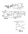
- Fig. 1 shows a free-running oscillator circuit comprising a NAND logic element or gate 10 having an input terminal 12 receiving an asynchronous control signal CS.
- An output terminal 14 of the NAND gate 10 is connected to an input terminal of a delay element 16 having a time delay of T2, while an output 18 of the delay element 16 is connected as a second input of the NAND gate 10.
- the CS control signal is enabled or high, the oscillator runs but when the CS signal is disabled or low, the oscillator output signal KS at the output terminal 14 of the NAND gate 10 remains high.
- the CS control signal therefore turns the oscillator on and off or synchronizes the oscillator output with the rising edge of the CS signal.
- a first transition from high to low of the KS output signal follows the transition of the CS control signal from low to high by one gate delay, the delay of the NAND logic element 10. Subsequent transitions of the KS clock signal occur after delay T2 plus the gate delay of the. NAND gate 10.
- the oscillator circuit of FIG. 1 represents the prior art which has a disadvantage of possible unstable operation due to a logic race condition when the CS control signal changes state at the same time the KS output of the NAND gate 10 changes. At such time a KS clock signal having less than acceptable pulse width can occur.
- a free-running clock synchronizer circuit in accordance with the present invention includes a transparent latch circuit 30 receiving a CS1 control signal on an input terminal 32.
- the latch circuit 30 may comprise a conventional storage element such as a D bistable or flip-flop.
- An output terminal 34 of the latch circuit 30, signal CSL, is connected as one input of a NAND logic element or gate 36, the output of which is the clock signal KS1.
- Clock signal KS1 is coupled to input terminal 37 of delay line 38 adapted to produce a first output at tap 40 after a time delay T1.
- This first output at tap 40 of the delay line 38, signal DL1 is connected as a first input of an AND gate 41 while a second output tap 44 of the delay line 38, signal DL2, is connected as a second input of the NAND gate 36.
- the delay at the second output tap 44 of the delay line 38 is T2, T2 being greater than T1.
- the CSL signal is connected as a second input of the AND gate 41, an output of which is supplied as a first input of a NAND gate 42.
- Tap 44 of the delay line 38 further provides a second input to WAND gate 42 via an inverter 46, and NAND gate 42 supplies a signal DLE at terminal 48 which is connected to a latch-enable input 50 of the latch circuit 30.
- the KS1 signal output of the WAND gate 36 is a square wave clock signal with a period 2 (T2 + D1) where D1 is the gate delay of the NAND gate 36.
- the latch circuit 30 functions normally as a transparent logic element that passes the CSI control signal directly. with only one gate delay, to the NAND gate 36 as control signal CSL on terminal 34.
- the CSL signal gates the KSI oscillator output signal on and off so the oscillator output signal is synchronized with the CS1 control signal.
- the enabling (high) output at terminal 48 of the NAND gate 42 normally enables the latch circuit 30 to pass the CS1 control signal as the CSL signal. But after the positive portion of the KS1 signal has traversed the delay line 38 and appears at the T1 output tap 40 as the DL1 signal, the CSL and DL1 signals enable the AND gate 41 which causes the DLE signal output at terminal 48 of the NAND gate 42 to go low for a period T2-T1 and disable latch 30, i.e. when a positive-to-negative transition of the KS1 signal may occur. As shown in FIG. 3, the CS1 signal might also be in transition from high to low during such period.
- the disabled latch circuit 30 then protects the oscillator circuit from an undefined or unstable logic condition of NAND gate 36 caused by the CS1 control signal changing state at or near the same time the KS1 output of the NAND gate 36 changes.
- the latch circuit 30 prevents KS1 from returning immediately to a positive level until after the DLE signal concludes and latch 30 generates the falling, edge of CSL.
- the circuit output is then synchronized with the rising edge of the CSL signal so that delaying the generation of the falling edge of the CSL signal does not adversely affect circuit operation. It is seen, however, that the circuit is prevented from generating pulses shorter than a given duration.
- FIG. 4 is an expansion of the potentially unstable period when the DLE signal is low, and shows the gate delays associated with the generation of a minimum-width negative transition of the KS1 clock signal.
- the protection circuit comprising the gates 41, 42, 46 and the latch circuit 30 ensures that a negative portion of the KS1 signal will have a length of at least three gate delays.
Landscapes
- Stabilization Of Oscillater, Synchronisation, Frequency Synthesizers (AREA)
Claims (2)
Applications Claiming Priority (2)
| Application Number | Priority Date | Filing Date | Title |
|---|---|---|---|
| US06/803,262 US4691121A (en) | 1985-11-29 | 1985-11-29 | Digital free-running clock synchronizer |
| US803262 | 1991-12-05 |
Publications (2)
| Publication Number | Publication Date |
|---|---|
| EP0225512A1 EP0225512A1 (fr) | 1987-06-16 |
| EP0225512B1 true EP0225512B1 (fr) | 1990-11-07 |
Family
ID=25186054
Family Applications (1)
| Application Number | Title | Priority Date | Filing Date |
|---|---|---|---|
| EP86115966A Expired EP0225512B1 (fr) | 1985-11-29 | 1986-11-17 | Circuit de synchronisation d'horloge numérique librement oscillante |
Country Status (5)
| Country | Link |
|---|---|
| US (1) | US4691121A (fr) |
| EP (1) | EP0225512B1 (fr) |
| JP (1) | JPS62131631A (fr) |
| CA (1) | CA1284363C (fr) |
| DE (1) | DE3675506D1 (fr) |
Families Citing this family (10)
| Publication number | Priority date | Publication date | Assignee | Title |
|---|---|---|---|---|
| JPH0821844B2 (ja) * | 1986-05-30 | 1996-03-04 | 三菱電機株式会社 | 半導体集積回路 |
| JPH0198313A (ja) * | 1987-10-09 | 1989-04-17 | Nec Corp | 同期化回路 |
| US4857868A (en) * | 1988-03-30 | 1989-08-15 | Rockwell International Corporation | Data driven clock generator |
| US5625316A (en) * | 1994-07-01 | 1997-04-29 | Motorola, Inc. | Tuning circuit for an RC filter |
| US6233205B1 (en) | 1996-09-17 | 2001-05-15 | Xilinx, Inc. | Built-in self test method for measuring clock to out delays |
| US6466520B1 (en) | 1996-09-17 | 2002-10-15 | Xilinx, Inc. | Built-in AC self test using pulse generators |
| JP3425876B2 (ja) * | 1999-01-07 | 2003-07-14 | エヌイーシーマイクロシステム株式会社 | パルス発生回路 |
| US6452459B1 (en) | 1999-07-22 | 2002-09-17 | Xilinx, Inc. | Circuit for measuring signal delays of synchronous memory elements |
| US6630838B1 (en) | 2001-01-23 | 2003-10-07 | Xilinx, Inc. | Method for implementing dynamic burn-in testing using static test signals |
| US7065684B1 (en) | 2002-04-18 | 2006-06-20 | Xilinx, Inc. | Circuits and methods for measuring signal propagation delays on integrated circuits |
Family Cites Families (7)
| Publication number | Priority date | Publication date | Assignee | Title |
|---|---|---|---|---|
| DE1160892B (de) * | 1959-10-06 | 1964-01-09 | Ibm | Schiebeeinheit |
| DE1276703B (de) * | 1966-07-01 | 1968-09-05 | Siemens Ag | Elektronischer Taktgenerator |
| US4134073A (en) * | 1976-07-12 | 1979-01-09 | Honeywell Information Systems Inc. | Clock system having adaptive synchronization feature |
| US4105978A (en) * | 1976-08-02 | 1978-08-08 | Honeywell Information Systems Inc. | Stretch and stall clock |
| US4544914A (en) * | 1979-12-17 | 1985-10-01 | Trw Inc. | Asynchronously controllable successive approximation analog-to-digital converter |
| US4386401A (en) * | 1980-07-28 | 1983-05-31 | Sperry Corporation | High speed processing restarting apparatus |
| JPS5760754A (en) * | 1980-09-27 | 1982-04-12 | Fujitsu Ltd | Synchronizing circuit |
-
1985
- 1985-11-29 US US06/803,262 patent/US4691121A/en not_active Expired - Fee Related
-
1986
- 1986-10-21 CA CA000520966A patent/CA1284363C/fr not_active Expired - Fee Related
- 1986-11-11 JP JP61268488A patent/JPS62131631A/ja active Pending
- 1986-11-17 DE DE8686115966T patent/DE3675506D1/de not_active Expired - Fee Related
- 1986-11-17 EP EP86115966A patent/EP0225512B1/fr not_active Expired
Also Published As
| Publication number | Publication date |
|---|---|
| CA1284363C (fr) | 1991-05-21 |
| JPS62131631A (ja) | 1987-06-13 |
| US4691121A (en) | 1987-09-01 |
| EP0225512A1 (fr) | 1987-06-16 |
| DE3675506D1 (de) | 1990-12-13 |
Similar Documents
| Publication | Publication Date | Title |
|---|---|---|
| US5600824A (en) | Clock generating means for generating bus clock and chip clock synchronously having frequency ratio of N-1/N responsive to synchronization signal for inhibiting data transfer | |
| US4703421A (en) | Ready line synchronization circuit for use in a duplicated computer system | |
| US5140680A (en) | Method and apparatus for self-timed digital data transfer and bus arbitration | |
| US4419629A (en) | Automatic synchronous switch for a plurality of asynchronous oscillators | |
| US4134073A (en) | Clock system having adaptive synchronization feature | |
| US5489865A (en) | Circuit for filtering asynchronous metastability of cross-coupled logic gates | |
| US4811282A (en) | Retiming circuit for pulse signals, particularly for microprocessor peripherals | |
| US4575644A (en) | Circuit for prevention of the metastable state in flip-flops | |
| US5793227A (en) | Synchronizing logic avoiding metastability | |
| US4386401A (en) | High speed processing restarting apparatus | |
| US4070630A (en) | Data transfer synchronizing circuit | |
| US5128970A (en) | Non-return to zero synchronizer | |
| US4691121A (en) | Digital free-running clock synchronizer | |
| US4317053A (en) | High speed synchronization circuit | |
| JP2695535B2 (ja) | タイマ入力制御回路及びカウンタ制御回路 | |
| US5758131A (en) | Bus adapter for synchronizing communications between two circuits running at different clock rates | |
| US4409671A (en) | Data processor having single clock pin | |
| EP0411759B1 (fr) | Dispositif de synchronisation utilisant l'extrapolation de la phase d'horloge | |
| US4823365A (en) | Synchronization method and elastic buffer circuit | |
| KR19980078161A (ko) | 반도체 메모리 소자의 딜레이 루프 럭크 회로 | |
| US3935475A (en) | Two-phase MOS synchronizer | |
| US5898640A (en) | Even bus clock circuit | |
| US6928574B1 (en) | System and method for transferring data from a lower frequency clock domain to a higher frequency clock domain | |
| US5315183A (en) | Synchronous phase detector circuit | |
| US4928290A (en) | Circuit for stable synchronization of asynchronous data |
Legal Events
| Date | Code | Title | Description |
|---|---|---|---|
| PUAI | Public reference made under article 153(3) epc to a published international application that has entered the european phase |
Free format text: ORIGINAL CODE: 0009012 |
|
| AK | Designated contracting states |
Kind code of ref document: A1 Designated state(s): DE FR GB NL |
|
| 17P | Request for examination filed |
Effective date: 19870825 |
|
| 17Q | First examination report despatched |
Effective date: 19890531 |
|
| GRAA | (expected) grant |
Free format text: ORIGINAL CODE: 0009210 |
|
| AK | Designated contracting states |
Kind code of ref document: B1 Designated state(s): DE FR GB NL |
|
| PGFP | Annual fee paid to national office [announced via postgrant information from national office to epo] |
Ref country code: NL Payment date: 19901130 Year of fee payment: 5 |
|
| ET | Fr: translation filed | ||
| PGFP | Annual fee paid to national office [announced via postgrant information from national office to epo] |
Ref country code: FR Payment date: 19901210 Year of fee payment: 5 |
|
| PGFP | Annual fee paid to national office [announced via postgrant information from national office to epo] |
Ref country code: GB Payment date: 19901212 Year of fee payment: 5 |
|
| REF | Corresponds to: |
Ref document number: 3675506 Country of ref document: DE Date of ref document: 19901213 |
|
| PGFP | Annual fee paid to national office [announced via postgrant information from national office to epo] |
Ref country code: DE Payment date: 19901231 Year of fee payment: 5 |
|
| PLBE | No opposition filed within time limit |
Free format text: ORIGINAL CODE: 0009261 |
|
| STAA | Information on the status of an ep patent application or granted ep patent |
Free format text: STATUS: NO OPPOSITION FILED WITHIN TIME LIMIT |
|
| 26N | No opposition filed | ||
| PG25 | Lapsed in a contracting state [announced via postgrant information from national office to epo] |
Ref country code: GB Effective date: 19911117 |
|
| PG25 | Lapsed in a contracting state [announced via postgrant information from national office to epo] |
Ref country code: NL Effective date: 19920601 |
|
| GBPC | Gb: european patent ceased through non-payment of renewal fee | ||
| NLV4 | Nl: lapsed or anulled due to non-payment of the annual fee | ||
| PG25 | Lapsed in a contracting state [announced via postgrant information from national office to epo] |
Ref country code: FR Effective date: 19920731 |
|
| PG25 | Lapsed in a contracting state [announced via postgrant information from national office to epo] |
Ref country code: DE Effective date: 19920801 |
|
| REG | Reference to a national code |
Ref country code: FR Ref legal event code: ST |