EP0225587B1 - Circuit pour régénérer et synchroniser un signal numérique - Google Patents
Circuit pour régénérer et synchroniser un signal numérique Download PDFInfo
- Publication number
- EP0225587B1 EP0225587B1 EP19860116757 EP86116757A EP0225587B1 EP 0225587 B1 EP0225587 B1 EP 0225587B1 EP 19860116757 EP19860116757 EP 19860116757 EP 86116757 A EP86116757 A EP 86116757A EP 0225587 B1 EP0225587 B1 EP 0225587B1
- Authority
- EP
- European Patent Office
- Prior art keywords
- line
- delay
- output
- clock
- unit
- Prior art date
- Legal status (The legal status is an assumption and is not a legal conclusion. Google has not performed a legal analysis and makes no representation as to the accuracy of the status listed.)
- Expired - Lifetime
Links
- 230000001172 regenerating effect Effects 0.000 title claims description 3
- 238000005070 sampling Methods 0.000 claims description 15
- 230000010363 phase shift Effects 0.000 claims description 7
- 230000001360 synchronised effect Effects 0.000 claims description 3
- 239000000872 buffer Substances 0.000 description 22
- 238000011156 evaluation Methods 0.000 description 7
- 238000010586 diagram Methods 0.000 description 4
- 230000008929 regeneration Effects 0.000 description 3
- 238000011069 regeneration method Methods 0.000 description 3
- 230000001133 acceleration Effects 0.000 description 2
- 230000003111 delayed effect Effects 0.000 description 2
- 230000002123 temporal effect Effects 0.000 description 2
- 241000183024 Populus tremula Species 0.000 description 1
- 230000005540 biological transmission Effects 0.000 description 1
- 230000001419 dependent effect Effects 0.000 description 1
- 238000011161 development Methods 0.000 description 1
- 230000018109 developmental process Effects 0.000 description 1
- 238000012544 monitoring process Methods 0.000 description 1
- 230000010355 oscillation Effects 0.000 description 1
- 230000000630 rising effect Effects 0.000 description 1
- 238000012360 testing method Methods 0.000 description 1
Images


Classifications
-
- H—ELECTRICITY
- H04—ELECTRIC COMMUNICATION TECHNIQUE
- H04L—TRANSMISSION OF DIGITAL INFORMATION, e.g. TELEGRAPHIC COMMUNICATION
- H04L7/00—Arrangements for synchronising receiver with transmitter
- H04L7/02—Speed or phase control by the received code signals, the signals containing no special synchronisation information
- H04L7/033—Speed or phase control by the received code signals, the signals containing no special synchronisation information using the transitions of the received signal to control the phase of the synchronising-signal-generating means, e.g. using a phase-locked loop
- H04L7/0337—Selecting between two or more discretely delayed clocks or selecting between two or more discretely delayed received code signals
-
- H—ELECTRICITY
- H03—ELECTRONIC CIRCUITRY
- H03K—PULSE TECHNIQUE
- H03K5/00—Manipulating of pulses not covered by one of the other main groups of this subclass
- H03K5/13—Arrangements having a single output and transforming input signals into pulses delivered at desired time intervals
- H03K5/135—Arrangements having a single output and transforming input signals into pulses delivered at desired time intervals by the use of time reference signals, e.g. clock signals
-
- H—ELECTRICITY
- H04—ELECTRIC COMMUNICATION TECHNIQUE
- H04L—TRANSMISSION OF DIGITAL INFORMATION, e.g. TELEGRAPHIC COMMUNICATION
- H04L25/00—Baseband systems
- H04L25/02—Details ; arrangements for supplying electrical power along data transmission lines
- H04L25/06—DC level restoring means; Bias distortion correction ; Decision circuits providing symbol by symbol detection
- H04L25/061—DC level restoring means; Bias distortion correction ; Decision circuits providing symbol by symbol detection providing hard decisions only; arrangements for tracking or suppressing unwanted low frequency components, e.g. removal of DC offset
Definitions
- the invention relates to a circuit arrangement according to the preamble of patent claim 1.
- the technical object of the invention is to implement a safe regeneration and synchronization of a digital signal.
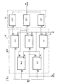
- the circuit arrangement according to the invention has a series circuit comprising a controllable delay line VZL and a decision logic EL.
- the decision logic EL is connected to a delay control unit VRE via a first control line UPO and a second control line DOWNO and the controllable delay line VZL via address lines S0, S1, S2, S3.
- the delay control unit VRE contains a presettable input PR, via which it can be set to predefinable states.
- the decision logic EL has a sampling circuit AS connected to a clock line TL and an evaluation unit AWE.
- the sampling circuit is supplied with a system clock CK via the clock line TL, the frequency of which corresponds to the bit rate of the digital signal to be regenerated and synchronized.
- the frequency of the system clock CK is 139.264 MHz.
- the evaluation unit AWE consists of a decoding unit DEC and a decision maker ENT which are connected to one another via five status lines U, D, O, F1, F2. Furthermore, the decision maker ENT of the evaluation unit AWE has a first status display output Z0 and a second status display output Z1 and is connected to the controllable delay line VZL via a first line BU and a second line BD.
- the decision maker ENT is via the first UPO and the second control line DOWNO to an input VE for the up-count direction or to an input RE for the down-count direction of an up-down counter VRZ the delay control unit VRE connected.
- the decision maker ENT and the up-down counter VRZ are supplied with an internal clock TI, which is derived from the system clock CK.
- the frequency of the internal clock TI is 1/8 times as high as the frequency of the system clock CK.
- Outputs A0, A1, A2, A3 of the up-down counter VRZ are connected to the controllable delay line VZL via the address lines S0, S1, S2, S3.
- the sampling circuit AS as shown in FIG. 2, consists of a three-stage phase shifter PS and a sampling / storage unit ASPE constructed from five buffers FF1, FF2, FF3, FFM, FFB.
- An output P1 of the first stage of the phase shifter PS is connected to a data input D1 of the first buffer store FF1
- an output P2 of the second stage of the phase shifter PS is connected to a data input D2 of the second buffer store FF2 and, in parallel, to a data input DM of the fourth buffer store FFM.
- An output P3 of the third stage of the phase shifter PS is connected to a data input D3 of the third buffer FF3.
- Each buffer store FF1, FF2, FF3, FFM, FFB is connected in parallel to the clock line TL via a clock input T1, T2, T3, TM, TB, the fourth buffer store FFM having an inverting clock input TM.
- the clocked buffers are implemented by so-called D flip-flops.
- phase shifter PS In a first implementation of the phase shifter PS, as shown in FIG. 2, three delay elements LZG1, LZG2, LZG3 are used, which are passed through in parallel by the incoming digital signal.
- the smallest phase difference is determined by the smallest delay difference between two delay elements.
- the phase shift ⁇ 1 by the first runtime element LZG1 must therefore always be smaller than the phase shift by the second runtime element LZG2 and this again smaller than the phase shift by the third runtime element LZG3.
- the delay elements can be implemented by lines of a certain length, by a shift register or by simple logic gates.
- phase shifter PS In a second implementation of the phase shifter PS according to a further embodiment according to the invention (not shown further), two delay elements LZG1, LZG2 are connected in series.
- a tap arranged in front of the first runtime element LZG1 forms the output P1 of the first stage
- a tap arranged between the first LZG1 and the second runtime element LZG2 forms the output P2 of the second stage
- a tap arranged after the second runtime element LZG2 forms the output P3 of the third Stage of the phase shifter PS. Since the incoming digital signal passes through the three stages in series, ⁇ 1 ⁇ 2 ⁇ 3 is always given.
- the incoming digital signal is transmitted to the decision logic EL via the controllable delay line VZL.
- it passes through the three-stage phase shifter PS and is scanned and stored by the first, second, third and fourth buffer stores FF1, FF2, FF3, FFM.
- the reading is carried out with the active edge of the system clock CK, whereby the inverting clock input TM of the fourth buffer FFM takes it over half a system clock period T / 2 earlier, with the passive edge taking over the signal value present.
- the fifth buffer store FFB takes over the signal value sampled one system clock cycle period T with each active system clock edge.
- the five buffers FF1, FF2, FF3, FFM, FFB with the active system clock edge at their data outputs Q1, Q2, Q3, QM, QB thus provide five signals that correspond to the data signal at times t + ⁇ t, t, t- ⁇ t, tT / 2, tT, where the regenerated data signal can be tapped at the data output Q2 of the second buffer store FF2.
- the value .DELTA.t results accordingly from the delay of the delay elements LZG1, LZG2, LZG3 of the phase shifter PS and T is the system clock period.
- first status line U means that the incoming digital signal is delayed in relation to the system clock CK
- second status line D means that the incoming digital signal must experience an acceleration in order to be synchronous with the system clock CK.
- a distorted signal with different (high-low) pulse widths is now correctly evaluated, as can be seen from the lower half of Table 1, in which, in addition to the times t 1, t 2, t 3, half a system clock period T / 2 earlier - point t M - and a whole system clock period T earlier - time t B - the digital signal is sampled.
- the signal at the output QM of the fourth buffer FFM corresponds to the sample at time t M and the signal at the output QB of the fifth buffer FFB corresponds to the sample at time t B.
- the fourth status line F1 is subjected to a logic "one" level and, in accordance with a detected falling edge, the fifth status line F2 is assigned a logic " One "level occupied.
- the third status line O is assigned a logic "one" level.
- a possible wrong sampling time due to different pulse widths of the signal is recognized by the additional signal states at times t B and t M.
- the system clock data phase relationships decoded by the decoding unit DEC are transmitted via the five status lines U, D, O, F1, F2 to the decision maker ENT, who additionally evaluates the presence of a minimum delay or a maximum delay of the delay line VZL, for which purpose it is transmitted via the first line BU or via the second line BD is connected to the controllable delay line VZL.
- the four states S, S2, S1, OS of the decision maker ENT can be removed at any time at the first status display output Z0 and at the second status display output Z1 and can be directed to a corresponding external unit for further monitoring, testing or evaluation of the circuit arrangement according to the invention.
- the decision maker ENT uses a control signal depending on the input variables present, which are present via the five status lines U, D, O, F1, F2, as well as via the first line BU and the second line BD first control line UPO or the second control line DOWNO sent to the delay control unit VRE.
- a counting pulse is given to the input VE for the up-count direction of the up-down counter VRZ via the first control line UPO.
- the decision maker ENT uses a reset line QR which is fed back to the decoding unit DEC - cf.
- Table 1, left column - the decoding unit DEC has been reset for the duration of a clock period of the internal clock TI in order to ensure that the counting pulse is carried out reliably.
- the counting pulse increases the count of the up-down counter VRZ by one, which results in a delay of the incoming digital signals with respect to the system clock CK as follows.
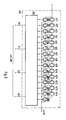
- FIG. 3 shows a delay line VZL constructed from fourteen delay elements VZ1, VZ2,..., VZ14 connected in series, the 0th to the 14th tap each having a controllable inverter IN0, IN1,..., IN14 the data output of the controllable delay line VZL is guided.
- a control unit AST is connected on the one hand to the controllable inverters IN0, IN1, ..., IN14 and on the other hand via the address lines S0, S1, S2, S3 to the outputs A0, A1, A2, A3 of the forward-reverse VRZ meter connected.
- the up-down counter VRZ is set to the counter reading 7 via the presettable input PR, this value is transmitted via the address lines S0, S1, S2, S3 to the control unit AST, which controls exactly the seventh inverter IN7, at the same time all the other inverters are blocked for data transmission.
- the digital signal therefore first passes through the first seven delay elements VZ1,..., VZ7, the seventh inverter IN7 and reaches the decision logic EL via the data output of the controllable delay line VZL.
- the counter reading is increased by one to the value eight by a counting pulse via the first control line UPO, this is forwarded to the control unit AST via the address lines S0, S1, S2, S3.
- the eighth inverter IN8 is now switched through, i.e. all other inverters including the seventh inverter IN7 are blocked.
- the digital signal is now delayed by the time of another delay element.
- a counting pulse is given via the second control line DOWNO by the decision maker ENT to the input RE of the up-down counter VRZ if, e.g. According to serial number 14 in Table 3, the digital signal must be accelerated.
- the evaluation of a minimum or a maximum delay of the delay line by the decision maker ENT prevents a possible oscillation of the delay line VZL between a maximum delay (fourteenth inverter IN14 switched through) and a minimum delay (zero inverter INO switched through, i.e. no delay element activated).
- the circuit arrangement according to the invention operates at any bit rates (typically: 140 Mbit / s) up to a maximum bit rate with a minimum bit length of T min , which is determined by the temporal resolution of the sampling circuit AS (transit time or transit time difference ⁇ t of the transit time elements LZG1, LZG2, LZG3) , by the temporal resolution of the delay line t VZL , by the deviation ⁇ Pw of the pulse width from the bit length T min and by the edge steepness t RF according to the relationship T min > t VZL + 2 ⁇ t + ⁇ Pw + t RF is determined.
Landscapes
- Engineering & Computer Science (AREA)
- Computer Networks & Wireless Communication (AREA)
- Signal Processing (AREA)
- Power Engineering (AREA)
- Physics & Mathematics (AREA)
- Nonlinear Science (AREA)
- Synchronisation In Digital Transmission Systems (AREA)
Claims (7)
- Agencement de circuit pour la régénération et la synchronisation d'un signal numérique à débit binaire élevé comprenant un circuit série, qui comporte une ligne à retard réglable (VZL) et une logique de décision (EL), parcourue par le signal numérique, la logique de décision (EL) étant raccordée via une première ligne de commande (UPO) et une deuxième ligne de commande (DOWNO) et la ligne à retard réglable (VZL) étant raccordée par des lignes d'adresse (S0, S1, S2, S3) à une unité de commande de retard (VRE), la logique de décision (EL) recevant un rythme de système (CK) via une ligne de cadencement (Tl) et donc la fréquence correspond au débit binaire du signal numérique à régénérer et dans lequel l'unité de commande du retard (VRE) est munie d'une entrée pré-réglable (PR) pour la détermination d'un état prédéterminé, caractérisé en ce que la logique de décision (EL) est munie d'un circuit d'échantillonnage (AS) raccordé à la ligne de cadencement (TL) et d'une unité d'analyse (AWE), au moyen desquels le signal numérique est échantillonné pendant au moins trois points séquentiels d'échantillonnage t - Δt, t, t + Δt, où Δt = intervalle d'échantillonnage, et en plus, à des instants temporels t - T/2 et t - T où T = période du rythme système, en étant ensuite analysé, pour la présence d'un bon rapport de phase rythme système/données sur la base des au moins trois intervalles séquentiels d'échantillonnage et pour savoir, en utilisant les instants d'échantillonnage supplémentaires, si un éventuel mauvais instant d'échantillonnage est présent à cause de différentes largeurs d'impulsion du signal, en ce que l'unité d'analyse (AWE) est munie d'une première sortie d'indication d'état (Z0) et d'une deuxième sortie d'indication d'état (Z1) et en ce que la ligne à retard réglable (VZL) est raccordée à l'unité d'analyse (AWE) au moyen d'une première ligne (BU) et d'une deuxième ligne (BD) permettant de transmettre la présence d'un retard minimal ou, respectivement, un retard maximal sur la ligne à retard (VZL) vers l'unité d'analyse (AWE).
- Agencement de circuit selon la revendication 1, caractérisé en ce que le circuit d'échantillonnage (AS) comporte un circuit de décalage de phase (PS) à trois étages et une unité d'échantillonnage/stockage (ASTE) composée de cinq mémoires intermédiaires (FF1, FF2, FF3, FFM, FFB), en ce qu'une sortie (P1) du premier étage du circuit de décalage de phase (TS) est reliée à une première entrée de données (T1) de la première mémoire intermédiaire (FF1), en ce qu'une sortie (P2) du deuxième étage du circuit de décalage de phase (PS) est raccordée à une entrée de données (PS) de la deuxième mémoire intermédiaire (FF2) et à une entrée de données (DM) de la quatrième mémoire intermédiaire (FFM), et en ce qu'une sortie (P3) du troisième étage du circuit de décalage de phase (PS) est raccordée à une entrée de données (D3) de la troisième mémoire intermédiaire (FF3), en ce qu'une sortie de données (Q2) de la deuxième mémoire intermédiaire (FF2) qui constitue la sortie de données de la logique de décision (EL) est raccordée à une entrée de données (DB) de la cinquième mémoire intermédiaire (FFB), en ce qu'une sortie de données (Q1, Q2, Q3, QM, QB) de chaque mémoire intermédiaire (FF1, FF2, FF3, FFM, FFB) est raccordée à l'unité d'analyse (AWE) et en ce que chaque mémoire intermédiaire (FF1, FF2, FF3, FFM, FFB) est munie d'une entrée de cadencement (T1, T2, T3, TM, TB) raccordée en parallèle sur la ligne de cadencement (TL), la quatrième mémoire intermédiaire (FFM) étant munie d'une entrée inversante de cadencement (TM).
- Agencement de circuit selon la revendication 2, caractérisé en ce que l'unité d'analyse (AWE) est munie d'une unité de décodage (DEC) et d'une unité de décision ENT, en ce que l'unité de décodage (DEC) est reliée, d'une part, aux sorties de données (Q1, Q2, Q3, QM, QB) des mémoires intermédiaires (FF1, FF2, FF3, FFM, FFB) de l'unité d'échantillonnage/stockage (ASTE) et, d'autre part, pour la retransmission des états décodés de signal, via cinq lignes d'état (U, D, O, F1, F2) à l'unité de décision (ENT), et en ce que l'unité de décision (ENT) et reliée via la première (UPO) et la deuxième (DOWNO) ligne de commande à l'unité de commande de retard (VRE) et via la première (BU) et la deuxième (BD) ligne à la ligne à retard réglable (VZL) de manière à ce que le rapport de phase signal/rythme système respectif peut être obtenu sur la première (Z0) et sur la deuxième (Z1) sortie d'indication d'état de l'unité de décision (ENT).
- Agencement de circuit selon la revendication 3, caractérisé en ce que l'unité de décision (ENT) et l'unité de commande de retard (VRE) reçoivent un rythme interne (TI) qui est obtenu à partir du rythme système (TK) et en ce que l'unité de décision (ENT) est rebouclée, via une ligne de remise à zéro (QR) sur l'unité de décodage (DEC) de manière à ce que lors de l'émission d'un signal de commande via la première (UPO) ou la deuxième (DOWNO) ligne de commande, l'unité de décodage (DEC) est remise à zéro pour la durée d'une période du rythme interne (TI).
- Agencement de circuit selon la revendication 2, caractérisé en ce les trois étages du circuit de décalage de phase (TS) sont constitués d'éléments de ligne à retard (LZG1, LZG2, LZG3) qui sont traversés en parallèles par le signal numérique dérivé, de manière à ce que le décalage de phase après passage par le premier élément de ligne à retard (LZG1) soit inférieur au décalage de phase après passage par le deuxième élément de ligne de retard (LZG2) et le décalage de phase après passage par le deuxième élément de ligne à retard (LZG2) soit inférieur au décalage de phase après passage par le troisième élément de ligne à retard (LZG3).
- Agencement de circuit selon la revendication 2, caractérisé en ce que le circuit de décalage de phase (PS) comporte des éléments de ligne à retard (LZG1, LZG2) raccordés en série, un point de prélèvement situé avant le premier élément de ligne à retard (LZG1) constituant la sortie (P1) du premier étage, un point de prélèvement situé entre le premier élément de ligne à retard (LZG1) et le deuxième élément de ligne à retard (LZG2) constituant la sortie (P2) du deuxième étage et un point de prélèvement situé après le deuxième élément de ligne à retard (LZG2) constituant la sortie (P3) du troisième étage du circuit de décalage de phase (PS) de manière à ce que le signal numérique dérivé traverse les trois étages l'un après l'autre.
- Agencement de circuit selon la revendication 3, caractérisé en ce que l'unité de commande de retard (VRE) est munie d'un compteur/décompteur (VRZ) accordé de manière synchrone au rythme interne et munie d'une entrée (PR) pré-réglable, en ce que la première ligne de commande (UPO) et la deuxième ligne de commande (DOWNO) sont raccordées à une entrée pour le centre de comptage avance (VE) et, respectivement, à une entrée pour le centre de comptage arrière (RE) du compteur/décompteur et en ce que la ligne à retard réglable (VZL) est reliée, via les lignes d'adresse (S0, S1, S2, S3) à des sorties (A0, A1, A2, A3) du compteur/décompteur (VRZ).
Applications Claiming Priority (2)
| Application Number | Priority Date | Filing Date | Title |
|---|---|---|---|
| DE19853543392 DE3543392A1 (de) | 1985-12-07 | 1985-12-07 | Schaltungsanordnung zum regenerieren und synchronisieren eines digitalen signales |
| DE3543392 | 1985-12-07 |
Publications (3)
| Publication Number | Publication Date |
|---|---|
| EP0225587A2 EP0225587A2 (fr) | 1987-06-16 |
| EP0225587A3 EP0225587A3 (fr) | 1991-04-10 |
| EP0225587B1 true EP0225587B1 (fr) | 1993-02-24 |
Family
ID=6287968
Family Applications (1)
| Application Number | Title | Priority Date | Filing Date |
|---|---|---|---|
| EP19860116757 Expired - Lifetime EP0225587B1 (fr) | 1985-12-07 | 1986-12-02 | Circuit pour régénérer et synchroniser un signal numérique |
Country Status (3)
| Country | Link |
|---|---|
| EP (1) | EP0225587B1 (fr) |
| DE (2) | DE3543392A1 (fr) |
| ES (1) | ES2003961A6 (fr) |
Families Citing this family (9)
| Publication number | Priority date | Publication date | Assignee | Title |
|---|---|---|---|---|
| DE3702614A1 (de) * | 1987-01-29 | 1988-08-11 | Standard Elektrik Lorenz Ag | Digitales koppelnetz fuer leitungs- und paketvermittlung und koppeleinrichtung hierzu |
| BE1000512A7 (nl) * | 1987-05-07 | 1989-01-10 | Bell Telephone Mfg | Schakelnetwerk. |
| WO1989009520A1 (fr) * | 1988-03-26 | 1989-10-05 | Alcatel N.V. | Circuit de synchronisation |
| DE3931259A1 (de) * | 1989-09-19 | 1991-03-28 | Siemens Ag | Verfahren zur fortlaufenden anpassung der phase eines digitalsignals an einen takt |
| DE59008700D1 (de) * | 1989-09-19 | 1995-04-20 | Siemens Ag | Synchronisiereinrichtung für ein Digitalsignal. |
| DE4025004A1 (de) * | 1990-08-07 | 1992-02-13 | Standard Elektrik Lorenz Ag | Schaltungsanordnung zum regenerieren und synchronisieren eines digitalen signals |
| EP0562183A1 (fr) * | 1992-03-27 | 1993-09-29 | ALCATEL BELL Naamloze Vennootschap | Méthode de synchronisation et dispositif utilisant une telle méthode |
| DE4434803C1 (de) * | 1994-09-29 | 1996-03-07 | Ant Nachrichtentech | Verfahren und Anordnung zur Abtastung eines seriellen Bitstromes |
| US6130566A (en) * | 1996-10-30 | 2000-10-10 | Yokomizo; Akira | Digital wave shaping circuit, frequency multiplying circuit, and external synchronizing method, and external synchronizing circuit |
Family Cites Families (1)
| Publication number | Priority date | Publication date | Assignee | Title |
|---|---|---|---|---|
| DE3441501A1 (de) * | 1984-11-14 | 1986-05-15 | Standard Elektrik Lorenz Ag, 7000 Stuttgart | Schaltungsanordnung zum regenerieren und synchronisieren eines digitalen signals |
-
1985
- 1985-12-07 DE DE19853543392 patent/DE3543392A1/de not_active Withdrawn
-
1986
- 1986-12-02 EP EP19860116757 patent/EP0225587B1/fr not_active Expired - Lifetime
- 1986-12-02 DE DE8686116757T patent/DE3687825D1/de not_active Expired - Fee Related
- 1986-12-05 ES ES8603299A patent/ES2003961A6/es not_active Expired
Also Published As
| Publication number | Publication date |
|---|---|
| DE3687825D1 (de) | 1993-04-01 |
| DE3543392A1 (de) | 1987-06-25 |
| ES2003961A6 (es) | 1988-12-01 |
| EP0225587A2 (fr) | 1987-06-16 |
| EP0225587A3 (fr) | 1991-04-10 |
Similar Documents
| Publication | Publication Date | Title |
|---|---|---|
| DE69106012T2 (de) | Rahmensynchronisierungsanordnung. | |
| DE68923207T2 (de) | Schaltung zur Verhinderung eines metastabilen Zustandes. | |
| DE69016169T2 (de) | Leitungschnittstelle für ein Nachrichtenübertragungsnetz. | |
| DE3246432C2 (fr) | ||
| EP0225587B1 (fr) | Circuit pour régénérer et synchroniser un signal numérique | |
| EP0345564B1 (fr) | Méthode et dispositif de récupération d'une horloge bit d'un signal de télécommunication numérique | |
| DE3442613C2 (fr) | ||
| DE60213443T2 (de) | Speicherschaltung und schaltung zur erkennung eines gültigen überganges | |
| DE3686902T2 (de) | Selbstpruefender zweikanal-anstiegsflanken-synchronisierer. | |
| CH651709A5 (de) | Verfahren und einrichtung zur entzerrung binaerer empfangssignale. | |
| DE2055356B2 (de) | Rastersynchronisierschaltung fuer digitale kommunikationssysteme | |
| DE2714219C2 (fr) | ||
| EP0363513A1 (fr) | Procedé et dispositif de réception d'un signal numérique binaire | |
| DE69120244T2 (de) | Synchronisierschaltung | |
| DE3441501A1 (de) | Schaltungsanordnung zum regenerieren und synchronisieren eines digitalen signals | |
| DE1252727B (de) | Verfahren zum störungsfreien Empfang übertragener Daten | |
| DE102004044815A1 (de) | Datenverarbeitungsvorrichtung mit Taktrückgewinnung aus unterschiedlichen Quellen | |
| EP0317829B1 (fr) | Méthode et appareil pour la génération d'un signal de correction pour un dispositif numérique récupération d'horloge | |
| EP0545493A2 (fr) | Circuit de balayage | |
| DE2242639B2 (de) | Zeitmultiplex-telegrafie-system fuer zeichenweise verschachtelung | |
| DE3924907A1 (de) | Redundante taktgeberanordnung | |
| DE3246211A1 (de) | Schaltungsanordnung zur detektion von folgen identischer binaerwerte | |
| DE69412332T2 (de) | Verfahren zur Beschleunigung der Synchronisierung einer Phasenregelschleife und entsprechende Phasenregelschleife | |
| DE19535007A1 (de) | Zählschaltung mit Ladefunktion | |
| DE10164837B4 (de) | Verarbeitung von digitalen Hochgeschwindigkeitssignalen |
Legal Events
| Date | Code | Title | Description |
|---|---|---|---|
| PUAI | Public reference made under article 153(3) epc to a published international application that has entered the european phase |
Free format text: ORIGINAL CODE: 0009012 |
|
| AK | Designated contracting states |
Kind code of ref document: A2 Designated state(s): BE DE FR IT NL |
|
| RAP1 | Party data changed (applicant data changed or rights of an application transferred) |
Owner name: ALCATEL N.V. Owner name: STANDARD ELEKTRIK LORENZ AKTIENGESELLSCHAFT |
|
| RAP3 | Party data changed (applicant data changed or rights of an application transferred) |
Owner name: ALCATEL N.V. Owner name: STANDARD ELEKTRIK LORENZ AKTIENGESELLSCHAFT |
|
| PUAL | Search report despatched |
Free format text: ORIGINAL CODE: 0009013 |
|
| AK | Designated contracting states |
Kind code of ref document: A3 Designated state(s): BE DE FR IT NL |
|
| 17P | Request for examination filed |
Effective date: 19910719 |
|
| 17Q | First examination report despatched |
Effective date: 19911119 |
|
| RAP3 | Party data changed (applicant data changed or rights of an application transferred) |
Owner name: ALCATEL N.V. Owner name: ALCATEL SEL AKTIENGESELLSCHAFT |
|
| GRAA | (expected) grant |
Free format text: ORIGINAL CODE: 0009210 |
|
| AK | Designated contracting states |
Kind code of ref document: B1 Designated state(s): BE DE FR IT NL |
|
| ITF | It: translation for a ep patent filed | ||
| REF | Corresponds to: |
Ref document number: 3687825 Country of ref document: DE Date of ref document: 19930401 |
|
| ET | Fr: translation filed | ||
| PGFP | Annual fee paid to national office [announced via postgrant information from national office to epo] |
Ref country code: BE Payment date: 19931223 Year of fee payment: 8 |
|
| PLBE | No opposition filed within time limit |
Free format text: ORIGINAL CODE: 0009261 |
|
| STAA | Information on the status of an ep patent application or granted ep patent |
Free format text: STATUS: NO OPPOSITION FILED WITHIN TIME LIMIT |
|
| 26N | No opposition filed | ||
| PG25 | Lapsed in a contracting state [announced via postgrant information from national office to epo] |
Ref country code: BE Effective date: 19941231 |
|
| BERE | Be: lapsed |
Owner name: ALCATEL N.V. Effective date: 19941231 |
|
| PGFP | Annual fee paid to national office [announced via postgrant information from national office to epo] |
Ref country code: NL Payment date: 20011120 Year of fee payment: 16 |
|
| PGFP | Annual fee paid to national office [announced via postgrant information from national office to epo] |
Ref country code: DE Payment date: 20011208 Year of fee payment: 16 |
|
| PGFP | Annual fee paid to national office [announced via postgrant information from national office to epo] |
Ref country code: FR Payment date: 20011211 Year of fee payment: 16 |
|
| PG25 | Lapsed in a contracting state [announced via postgrant information from national office to epo] |
Ref country code: NL Free format text: LAPSE BECAUSE OF NON-PAYMENT OF DUE FEES Effective date: 20030701 Ref country code: DE Free format text: LAPSE BECAUSE OF NON-PAYMENT OF DUE FEES Effective date: 20030701 |
|
| NLV4 | Nl: lapsed or anulled due to non-payment of the annual fee |
Effective date: 20030701 |
|
| PG25 | Lapsed in a contracting state [announced via postgrant information from national office to epo] |
Ref country code: FR Free format text: LAPSE BECAUSE OF NON-PAYMENT OF DUE FEES Effective date: 20030901 |
|
| REG | Reference to a national code |
Ref country code: FR Ref legal event code: ST |
|
| PG25 | Lapsed in a contracting state [announced via postgrant information from national office to epo] |
Ref country code: IT Free format text: LAPSE BECAUSE OF NON-PAYMENT OF DUE FEES;WARNING: LAPSES OF ITALIAN PATENTS WITH EFFECTIVE DATE BEFORE 2007 MAY HAVE OCCURRED AT ANY TIME BEFORE 2007. THE CORRECT EFFECTIVE DATE MAY BE DIFFERENT FROM THE ONE RECORDED. Effective date: 20051202 |