EP0225968A2 - Quasi-analoge Wiederherstellung eines in Amplitude und Frequenz veränderlichen Eingangssignals - Google Patents
Quasi-analoge Wiederherstellung eines in Amplitude und Frequenz veränderlichen Eingangssignals Download PDFInfo
- Publication number
- EP0225968A2 EP0225968A2 EP86111212A EP86111212A EP0225968A2 EP 0225968 A2 EP0225968 A2 EP 0225968A2 EP 86111212 A EP86111212 A EP 86111212A EP 86111212 A EP86111212 A EP 86111212A EP 0225968 A2 EP0225968 A2 EP 0225968A2
- Authority
- EP
- European Patent Office
- Prior art keywords
- bits
- discrete
- voltage
- input signal
- analog
- Prior art date
- Legal status (The legal status is an assumption and is not a legal conclusion. Google has not performed a legal analysis and makes no representation as to the accuracy of the status listed.)
- Withdrawn
Links
Images


Classifications
-
- H—ELECTRICITY
- H04—ELECTRIC COMMUNICATION TECHNIQUE
- H04B—TRANSMISSION
- H04B14/00—Transmission systems not characterised by the medium used for transmission
- H04B14/02—Transmission systems not characterised by the medium used for transmission characterised by the use of pulse modulation
- H04B14/04—Transmission systems not characterised by the medium used for transmission characterised by the use of pulse modulation using pulse code modulation
-
- G—PHYSICS
- G11—INFORMATION STORAGE
- G11B—INFORMATION STORAGE BASED ON RELATIVE MOVEMENT BETWEEN RECORD CARRIER AND TRANSDUCER
- G11B20/00—Signal processing not specific to the method of recording or reproducing; Circuits therefor
- G11B20/10—Digital recording or reproducing
- G11B20/10527—Audio or video recording; Data buffering arrangements
-
- H—ELECTRICITY
- H03—ELECTRONIC CIRCUITRY
- H03M—CODING; DECODING; CODE CONVERSION IN GENERAL
- H03M1/00—Analogue/digital conversion; Digital/analogue conversion
- H03M1/10—Calibration or testing
- H03M1/1009—Calibration
- H03M1/1033—Calibration over the full range of the converter, e.g. for correcting differential non-linearity
- H03M1/1038—Calibration over the full range of the converter, e.g. for correcting differential non-linearity by storing corrected or correction values in one or more digital look-up tables
- H03M1/1047—Calibration over the full range of the converter, e.g. for correcting differential non-linearity by storing corrected or correction values in one or more digital look-up tables using an auxiliary digital/analogue converter for adding the correction values to the analogue signal
Definitions
- This invention relates to methods and apparatus for producing practical high level quasi-analog reconstructions of original analog signals of continuously varying amplitude and frequency.
- Quasi-analog reconstructions of original amplitude and frequency varying analog signals have been provided heretofore in communication systems by sampling, quantizing and encoding an audio input signal into digital signals and using the binary hits of the digital signal of each sampling period to switch discrete voltages supplied from respective power sources into or out of a series voltage summation output line.
- the output voltages thus produced in successive sampling periods provide the desired quasi-analog reconstruction of the audio input signal.
- An aim of the invention is to provide new and improved techniques leading to the production of a high level quasi-analog reconstruction of an amplitude and frequency varying analog input signal.
- Another aim of the invention consonant with the foregoing aim, is to produce the reconstructed signal in stepwise fashion and with optimum resolution resulting from a unique utilization of a basic PCM signal derived from the analog input signal.
- Another aim of the invention is to process a basic PCM signal into discrete decimal and binary steps leading to a practical reconstruction of an original analog signal in small discrete steps, the reconstructed analog signal being advantageously suitable for a number of purposes including the amplitude modulating of a radio frequency amplifier stage in order to obtain a low distortion, high efficiency AM signal.
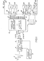
- a basic pulse code modulation signal having a plurality of C parallel binary bits is generated by an analog-to-digital converter 2 which, according to well-known pulse code modulation techniques, receives its analog input from a sample and hold circuit 4 to which an analog input signal 6 of continuously-varying amplitude and frequency is fed, this signal ultimately to undergo a quasi-analog reconstruction.
- the sampling rate is determined in conventional manner by a timing generator 8 which supplies timing pulses to the sample and hold circuit 4 and to the analog-to-digital converter 2, the rate being at least twice the highest frequency in the analog input signal 6.
- the instanteous magnitudes of the time-varying amplitude of the analog input signal 6 are measured at a given sampling rate, and successive proportional responses in pulse code form are supplied by the analog-to-digital converter 2, each codeword having a length of C parallel binary bits.
- the first or most significant group of A bits of the C bits is channeled to the input of a binary-to-discrete decimal step converter 10 which converts the A bits into a set of (2A - 1) parallel data appearing on respective control lines 12 at the output of the converter 10. Accordingly, the converter 10 has a plurality of (2-1) control lines 12, each receiving a respective one of the (2 A -1) data outputted by the converter 10.
- the (2A - 1) parallel data and the B bits are utilized to switchably interconnect, in series, D.C. voltage outputs of respectively associated discrete voltage sources such that a resultant summation output E out is produced which is an analog voltage corresponding in magnitude to the value of the C bit codeword.
- a plurality of (2A - 1) switches 16 are respectively controlled by the control lines 12, each switch 16 being connected to a respective voltage source 18 of V c volts D.C., where and Vmax is substantially the peak voltage amplitude to be provided in the quasi-analog reconstruction of the analog input signal 6.
- the control is such that all those switches 16 which are switched ON by their respective control lines 12 serially interconnect into a voltage summation line 20, the V volt outputs of the voltage sources 18 connected to those ON switches.
- the switches 16 which are switched OFF by their respective control lines isolate the V c volt outputs of the voltage sources 18 connected to the OFF switches from the serially interconnected V c volt outputs and maintain the serial continuity of the summation line 20 where the isolated outputs would otherwise be serially interconnected into the line.
- a plurality of B ON-OFF switches 22, which may be identical to the switches 16, are respectively controlled by the control lines 14, each switch 22 being connected to a respective voltage source 24.
- the voltage sources 24 respectively supply D.C.
- the voltages serially interconnected in the summation line 20 additively combine with one another to produce an output voltage E out across tHe end terminals 26, 28 of the line 20, each output voltage E out being a discrete voltage step in a staircase-type of quasi-analog reproduction of the analog input signal 6.
- the outputs of the five voltage sources 24 decrease in value in one-half voltage increments, i.e., 150, 75, 37.5, 18.75 and 9.375 volts and when such outputs are added to ⁇ V , there is achieved a total output capability of 38,390.625 volts with a 9.375 volt resolution, or a resolution of 1 part in 4095.
- the plurality of B ON-OFF switches 22 are still respectively controlled by the control lines 14, and the switches 22 are still respectively connected to voltage sources 24 whose D.C. voltages decline in one-half voltage increments from Vc/2 to Vc/2B according to the significance of the bits on the respective control lines 14.
- Fig. 3 illustrates a system capable of effectively handling the small voltage steps and distinguished by having no practical restriction on its maximum bit capacity.
- the system of Fig. 3 is similar to that of Fig. 1, particularly in its use of the binary-to-discrete decimal step converter 10 to convert A bits of the C-bit codeword representing each sample taken of the analog input signal 6 (Fig. 1) to (2 -1) discrete decimal data on control lines 12 associated with the switches 16 and the sources 18 of equal voltages V .
- the Fig. 3 system differs from the Fig.
- the B bits of the C-bit codeword by virtue of using the B bits of the C-bit codeword in two groups, one group having a plurality of N most significant bits, the other group having a plurality of (B-N) least significant bits. While the N bits are used in the Fig. 3 system in the same manner as all the B bits are used in the Fig. 1 system, i.e., to control the respective switches 22 associated with voltage sources 24 whose outputs decline in one-half voltage increments starting with an output of Vc/2, the (B-N) bits are uniquely handled by being fed to a D/A converter-step voltage follower circuit 30.
- the circuit 30, in response to 2 (B-N) possible binary values of the combination of (B-N) bits, is capable of producing 2 (B-N) analog voltage outputs which decline in one-half voltage increments from Vc/2 N+1 to 2 in step with respective decreases in the possible binary values of the (B-N) bit combination.
- the converter portion of the circuit 30 is provided by the digital-to-analog converter 32 which is shown in Fig. 3 as receiving (B-N) LSB's of the B bits channelled away from the C bits provided by the analog-to-digital converter 2 (Fig. 1).
- the step voltage follower portion of the circuit 30 is provided by an operational amplifier 34, a transistor 36 and a power supply 38.
- the analog voltage output of the converter 32 is fed via a lead 40 to the positive input terminal of the amplifier 34.
- the signal output of the amplifier 34 is applied via a lead 42 to the base of the transistor 36, the collector of which is connected directly to the power supply 38 via a lead 44 while the output of the transistor 36 is taken from the emitter thereof and applied to the voltage summation line 20 via a lead 46, whereby the transistor functions as an emitter-follower. Negative feedback from the emitter lead 46 to the negative input terminal of the amplifier 34 is conducted by a lead 48.
- the power supply 38 may provide approximately the same voltage magnitude Vc/2 N provided by that one of the voltage sources 2 24 which is correlated with the Nth bit of the N MSB's.
Landscapes
- Engineering & Computer Science (AREA)
- Signal Processing (AREA)
- Multimedia (AREA)
- Computer Networks & Wireless Communication (AREA)
- Physics & Mathematics (AREA)
- Nonlinear Science (AREA)
- Theoretical Computer Science (AREA)
- Analogue/Digital Conversion (AREA)
Applications Claiming Priority (2)
| Application Number | Priority Date | Filing Date | Title |
|---|---|---|---|
| US06/811,070 US4724420A (en) | 1985-12-19 | 1985-12-19 | Method and apparatus for quasi-analog reconstructions of amplitude and frequency varying analog input signals |
| US811070 | 2004-03-29 |
Publications (2)
| Publication Number | Publication Date |
|---|---|
| EP0225968A2 true EP0225968A2 (de) | 1987-06-24 |
| EP0225968A3 EP0225968A3 (de) | 1990-01-17 |
Family
ID=25205468
Family Applications (1)
| Application Number | Title | Priority Date | Filing Date |
|---|---|---|---|
| EP86111212A Withdrawn EP0225968A3 (de) | 1985-12-19 | 1986-08-13 | Quasi-analoge Wiederherstellung eines in Amplitude und Frequenz veränderlichen Eingangssignals |
Country Status (3)
| Country | Link |
|---|---|
| US (1) | US4724420A (de) |
| EP (1) | EP0225968A3 (de) |
| JP (1) | JPS62147817A (de) |
Families Citing this family (9)
| Publication number | Priority date | Publication date | Assignee | Title |
|---|---|---|---|---|
| US4979188A (en) * | 1988-04-29 | 1990-12-18 | Motorola, Inc. | Spectrally efficient method for communicating an information signal |
| US5200707A (en) * | 1990-06-05 | 1993-04-06 | Continental Electronics Corporation | Amplifier with multiple switched stages and noise suppression |
| US5099203A (en) * | 1990-06-05 | 1992-03-24 | Continental Electronics Corporation | Power amplifier having multiple switched stages and method of operating same |
| US6118399A (en) * | 1998-03-30 | 2000-09-12 | Silicon Laboratories, Inc. | Coarse/fine switching on digital-to-analog conversion output |
| KR101269855B1 (ko) * | 2011-10-12 | 2013-06-17 | 주식회사 글로리이앤씨 | 디지털 아날로그 변환장치 |
| US9455732B2 (en) * | 2014-12-19 | 2016-09-27 | Stmicroelectronics S.R.L. | Method and device for analog-to-digital conversion of signals, corresponding apparatus |
| US12276420B2 (en) | 2016-02-03 | 2025-04-15 | Strong Force Iot Portfolio 2016, Llc | Industrial internet of things smart heating systems and methods that produce and use hydrogen fuel |
| US20200133254A1 (en) | 2018-05-07 | 2020-04-30 | Strong Force Iot Portfolio 2016, Llc | Methods and systems for data collection, learning, and streaming of machine signals for part identification and operating characteristics determination using the industrial internet of things |
| EP3909223B1 (de) | 2019-01-13 | 2024-08-21 | Strong Force Iot Portfolio 2016, LLC | Überwachung und verwaltung von industriellen einstellungen |
Family Cites Families (14)
| Publication number | Priority date | Publication date | Assignee | Title |
|---|---|---|---|---|
| US3044007A (en) * | 1958-04-10 | 1962-07-10 | North American Aviation Inc | Programmable power supply |
| NL281663A (de) * | 1961-08-01 | |||
| US3217147A (en) * | 1961-11-28 | 1965-11-09 | Bell Telephone Labor Inc | Cumulative type decoder |
| US3305855A (en) * | 1962-11-08 | 1967-02-21 | Nippon Electric Co | Encoder and a decoder with nonlinear quantization |
| US3603971A (en) * | 1968-08-06 | 1971-09-07 | Perkin Elmer Corp | Apparatus for converting between digital and analog information |
| US3581076A (en) * | 1969-07-17 | 1971-05-25 | Sperry Rand Corp | Digital to analog current distribution circuit |
| US3877021A (en) * | 1971-04-23 | 1975-04-08 | Western Electric Co | Digital-to-analog converter |
| US3723855A (en) * | 1971-08-16 | 1973-03-27 | Sybron Corp | System having fast plural high voltage switching |
| US3892977A (en) * | 1973-01-29 | 1975-07-01 | Amp Inc | Switchable high voltage power supply |
| JPS5916443B2 (ja) * | 1976-02-06 | 1984-04-16 | ソニー株式会社 | パワ−アンプ |
| US4160244A (en) * | 1976-02-25 | 1979-07-03 | National Semiconductor Corporation | Conversion circuit |
| GB2064901B (en) * | 1979-11-30 | 1984-11-07 | Harris Corp | Digital high power amplifier |
| US4549166A (en) * | 1981-03-25 | 1985-10-22 | Hitachi, Ltd. | Digital-to-analog converter using a feedback element matching technique |
| US4580111A (en) * | 1981-12-24 | 1986-04-01 | Harris Corporation | Amplitude modulation using digitally selected carrier amplifiers |
-
1985
- 1985-12-19 US US06/811,070 patent/US4724420A/en not_active Expired - Lifetime
-
1986
- 1986-08-13 EP EP86111212A patent/EP0225968A3/de not_active Withdrawn
- 1986-08-27 JP JP61199166A patent/JPS62147817A/ja active Pending
Also Published As
| Publication number | Publication date |
|---|---|
| US4724420A (en) | 1988-02-09 |
| EP0225968A3 (de) | 1990-01-17 |
| JPS62147817A (ja) | 1987-07-01 |
Similar Documents
| Publication | Publication Date | Title |
|---|---|---|
| KR100436357B1 (ko) | 다중출력단을갖는디지털아날로그변환기및그변환방법 | |
| EP0141386B1 (de) | Digital-Analog-Umsetzer | |
| EP0249986A3 (de) | Analog-Digital-Wandler | |
| EP0225968A2 (de) | Quasi-analoge Wiederherstellung eines in Amplitude und Frequenz veränderlichen Eingangssignals | |
| GB2067373A (en) | Offset digital dither generator | |
| ATE25794T1 (de) | Analog-digital umwandler. | |
| US6359576B1 (en) | Apparatus and methods for performing RMS-to-DC conversion with bipolar input signal range | |
| WO1988001115A1 (en) | Current-steering digital-to-analog converter for providing bi-directional currents through a load | |
| GB2096848A (en) | -law/a-law pcm converter | |
| EP0112180A3 (de) | Nach dem Parallelverfahren arbeitender Analog-Digitalwandler | |
| EP1028530A3 (de) | Mehrkanaliges, paralleles, aufeinander abgestimmtes Digital-Analog-Wandlungsverfahren und Wandler, und damit versehene analoge Treiberschaltung | |
| GB2217128A (en) | D/a converter for 2's complement digital signals | |
| US3789389A (en) | Method and circuit for combining digital and analog signals | |
| US4143363A (en) | Nonuniform translation between analog and digital signals by a piece-wise linear process | |
| US3599204A (en) | Technique for high speed analog-to-digital conversion | |
| NO863761L (no) | Fremgangsmaate til digital-analog-omforming av digitale informasjoner til bipolare analogsignaler. | |
| AU558047B2 (en) | Analog to digital converter | |
| JPS5725722A (en) | Analog-to-digital converter | |
| US3315251A (en) | Encoding device with non-linear quantization | |
| Schoeff | A monolithic companding D/A converter | |
| US5684483A (en) | Floating point digital to analog converter | |
| SU1182671A1 (ru) | Преобразователь сигналов датчиков переменного тока | |
| JPS54152953A (en) | Digital-to-analog converter circuit | |
| SU978313A1 (ru) | Цифровой генератор синусоидального сигнала | |
| JPS59141827A (ja) | アナログ・デジタル変換制御装置 |
Legal Events
| Date | Code | Title | Description |
|---|---|---|---|
| PUAI | Public reference made under article 153(3) epc to a published international application that has entered the european phase |
Free format text: ORIGINAL CODE: 0009012 |
|
| AK | Designated contracting states |
Kind code of ref document: A2 Designated state(s): CH DE FR GB LI |
|
| PUAL | Search report despatched |
Free format text: ORIGINAL CODE: 0009013 |
|
| RHK1 | Main classification (correction) |
Ipc: H03F 3/217 |
|
| AK | Designated contracting states |
Kind code of ref document: A3 Designated state(s): CH DE FR GB LI |
|
| 17P | Request for examination filed |
Effective date: 19900220 |
|
| STAA | Information on the status of an ep patent application or granted ep patent |
Free format text: STATUS: THE APPLICATION IS DEEMED TO BE WITHDRAWN |
|
| 18D | Application deemed to be withdrawn |
Effective date: 19920303 |
|
| RIN1 | Information on inventor provided before grant (corrected) |
Inventor name: WOODARD, GEORGE W. |