EP0226517A2 - Procédé pour isoler des régions ayant des concentrations d'impuretés différentes dans un substrat semi-conducteur - Google Patents
Procédé pour isoler des régions ayant des concentrations d'impuretés différentes dans un substrat semi-conducteur Download PDFInfo
- Publication number
- EP0226517A2 EP0226517A2 EP86402837A EP86402837A EP0226517A2 EP 0226517 A2 EP0226517 A2 EP 0226517A2 EP 86402837 A EP86402837 A EP 86402837A EP 86402837 A EP86402837 A EP 86402837A EP 0226517 A2 EP0226517 A2 EP 0226517A2
- Authority
- EP
- European Patent Office
- Prior art keywords
- layer
- substrate
- oxide
- masking material
- opening
- Prior art date
- Legal status (The legal status is an assumption and is not a legal conclusion. Google has not performed a legal analysis and makes no representation as to the accuracy of the status listed.)
- Withdrawn
Links
Images

Classifications
-
- H—ELECTRICITY
- H10—SEMICONDUCTOR DEVICES; ELECTRIC SOLID-STATE DEVICES NOT OTHERWISE PROVIDED FOR
- H10P—GENERIC PROCESSES OR APPARATUS FOR THE MANUFACTURE OR TREATMENT OF DEVICES COVERED BY CLASS H10
- H10P50/00—Etching of wafers, substrates or parts of devices
- H10P50/69—Etching of wafers, substrates or parts of devices using masks for semiconductor materials
- H10P50/691—Etching of wafers, substrates or parts of devices using masks for semiconductor materials for Group V materials or Group III-V materials
- H10P50/693—Etching of wafers, substrates or parts of devices using masks for semiconductor materials for Group V materials or Group III-V materials characterised by their size, orientation, disposition, behaviour or shape, in horizontal or vertical plane
- H10P50/695—Etching of wafers, substrates or parts of devices using masks for semiconductor materials for Group V materials or Group III-V materials characterised by their size, orientation, disposition, behaviour or shape, in horizontal or vertical plane characterised by the process involved to create the mask, e.g. lift-off masks or sidewalls or to modify the mask
-
- H—ELECTRICITY
- H10—SEMICONDUCTOR DEVICES; ELECTRIC SOLID-STATE DEVICES NOT OTHERWISE PROVIDED FOR
- H10D—INORGANIC ELECTRIC SEMICONDUCTOR DEVICES
- H10D84/00—Integrated devices formed in or on semiconductor substrates that comprise only semiconducting layers, e.g. on Si wafers or on GaAs-on-Si wafers
- H10D84/01—Manufacture or treatment
- H10D84/0123—Integrating together multiple components covered by H10D12/00 or H10D30/00, e.g. integrating multiple IGBTs
- H10D84/0126—Integrating together multiple components covered by H10D12/00 or H10D30/00, e.g. integrating multiple IGBTs the components including insulated gates, e.g. IGFETs
- H10D84/0165—Integrating together multiple components covered by H10D12/00 or H10D30/00, e.g. integrating multiple IGBTs the components including insulated gates, e.g. IGFETs the components including complementary IGFETs, e.g. CMOS devices
- H10D84/0188—Manufacturing their isolation regions
-
- H—ELECTRICITY
- H10—SEMICONDUCTOR DEVICES; ELECTRIC SOLID-STATE DEVICES NOT OTHERWISE PROVIDED FOR
- H10D—INORGANIC ELECTRIC SEMICONDUCTOR DEVICES
- H10D84/00—Integrated devices formed in or on semiconductor substrates that comprise only semiconducting layers, e.g. on Si wafers or on GaAs-on-Si wafers
- H10D84/01—Manufacture or treatment
- H10D84/02—Manufacture or treatment characterised by using material-based technologies
- H10D84/03—Manufacture or treatment characterised by using material-based technologies using Group IV technology, e.g. silicon technology or silicon-carbide [SiC] technology
- H10D84/038—Manufacture or treatment characterised by using material-based technologies using Group IV technology, e.g. silicon technology or silicon-carbide [SiC] technology using silicon technology, e.g. SiGe
-
- H—ELECTRICITY
- H10—SEMICONDUCTOR DEVICES; ELECTRIC SOLID-STATE DEVICES NOT OTHERWISE PROVIDED FOR
- H10P—GENERIC PROCESSES OR APPARATUS FOR THE MANUFACTURE OR TREATMENT OF DEVICES COVERED BY CLASS H10
- H10P50/00—Etching of wafers, substrates or parts of devices
- H10P50/69—Etching of wafers, substrates or parts of devices using masks for semiconductor materials
- H10P50/691—Etching of wafers, substrates or parts of devices using masks for semiconductor materials for Group V materials or Group III-V materials
- H10P50/693—Etching of wafers, substrates or parts of devices using masks for semiconductor materials for Group V materials or Group III-V materials characterised by their size, orientation, disposition, behaviour or shape, in horizontal or vertical plane
- H10P50/696—Process specially adapted to improve the resolution of the mask
-
- H—ELECTRICITY
- H10—SEMICONDUCTOR DEVICES; ELECTRIC SOLID-STATE DEVICES NOT OTHERWISE PROVIDED FOR
- H10P—GENERIC PROCESSES OR APPARATUS FOR THE MANUFACTURE OR TREATMENT OF DEVICES COVERED BY CLASS H10
- H10P76/00—Manufacture or treatment of masks on semiconductor bodies, e.g. by lithography or photolithography
- H10P76/40—Manufacture or treatment of masks on semiconductor bodies, e.g. by lithography or photolithography of masks comprising inorganic materials
- H10P76/408—Manufacture or treatment of masks on semiconductor bodies, e.g. by lithography or photolithography of masks comprising inorganic materials characterised by their sizes, orientations, dispositions, behaviours or shapes
- H10P76/4085—Manufacture or treatment of masks on semiconductor bodies, e.g. by lithography or photolithography of masks comprising inorganic materials characterised by their sizes, orientations, dispositions, behaviours or shapes characterised by the processes involved to create the masks
-
- H—ELECTRICITY
- H10—SEMICONDUCTOR DEVICES; ELECTRIC SOLID-STATE DEVICES NOT OTHERWISE PROVIDED FOR
- H10W—GENERIC PACKAGES, INTERCONNECTIONS, CONNECTORS OR OTHER CONSTRUCTIONAL DETAILS OF DEVICES COVERED BY CLASS H10
- H10W10/00—Isolation regions in semiconductor bodies between components of integrated devices
- H10W10/01—Manufacture or treatment
- H10W10/011—Manufacture or treatment of isolation regions comprising dielectric materials
- H10W10/014—Manufacture or treatment of isolation regions comprising dielectric materials using trench refilling with dielectric materials, e.g. shallow trench isolations
-
- H—ELECTRICITY
- H10—SEMICONDUCTOR DEVICES; ELECTRIC SOLID-STATE DEVICES NOT OTHERWISE PROVIDED FOR
- H10W—GENERIC PACKAGES, INTERCONNECTIONS, CONNECTORS OR OTHER CONSTRUCTIONAL DETAILS OF DEVICES COVERED BY CLASS H10
- H10W10/00—Isolation regions in semiconductor bodies between components of integrated devices
- H10W10/01—Manufacture or treatment
- H10W10/041—Manufacture or treatment of isolation regions comprising polycrystalline semiconductor materials
-
- H—ELECTRICITY
- H10—SEMICONDUCTOR DEVICES; ELECTRIC SOLID-STATE DEVICES NOT OTHERWISE PROVIDED FOR
- H10W—GENERIC PACKAGES, INTERCONNECTIONS, CONNECTORS OR OTHER CONSTRUCTIONAL DETAILS OF DEVICES COVERED BY CLASS H10
- H10W10/00—Isolation regions in semiconductor bodies between components of integrated devices
- H10W10/10—Isolation regions comprising dielectric materials
- H10W10/17—Isolation regions comprising dielectric materials formed using trench refilling with dielectric materials, e.g. shallow trench isolations
-
- H—ELECTRICITY
- H10—SEMICONDUCTOR DEVICES; ELECTRIC SOLID-STATE DEVICES NOT OTHERWISE PROVIDED FOR
- H10W—GENERIC PACKAGES, INTERCONNECTIONS, CONNECTORS OR OTHER CONSTRUCTIONAL DETAILS OF DEVICES COVERED BY CLASS H10
- H10W10/00—Isolation regions in semiconductor bodies between components of integrated devices
- H10W10/40—Isolation regions comprising polycrystalline semiconductor materials
Definitions
- the present invention is directed to the manufacture of monolithic integrated circuits, and more particularly to the isolation of adjacent areas of different impurity concentration, such as the substrate and wells in CMOS transistor circuits.
- a barrier of an insulating material such as oxide or undoped polysilicon between them.
- an oxide barrier is typically provided around the p-type well that is diffused into the n-type body, to effectively isolate the NMOS transistor formed in the well from the complementary PMOS transistor in the body, and thereby prevent latch-up. Because of the presence of this barrier, it becomes possible to place the two complementary transistors closer to one another on the substrate, and thereby increase the packing density of transistors on the integrated circuit chip.
- the doping of the substrate to form the well and the formation of the barrier around the well were carried out in separate processing steps that utilized different photomasks to define the well and the barrier, respectively. Because of the relationship of the barrier to the well, the two masks that were used to form these adjacent areas in the substrate necessarily had to be aligned with one another.
- Figures 1A and 1B are a cross-sectional side view and a schematic circuit diagram, respectively, of a CMOS inverter circuit.
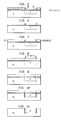
- Figures 2-11 sequentially illustrate the process steps that are used to form an oxide barrier between a well and a substrate in a CMOS circuit without the need for separate, aligned masks.
- CMOS complementary metal-oxide-semiconductor
- the source and drain electrodes S1 and D1 of one of the transistors are directly formed in an n-type substrate 10 by implanting a p-type impurity into two regions 12 of the substrate.
- a p-type region, or well 14 is formed in the substrate 10.
- the source and drain electrodes S2 and D2 of this second transistor are formed by implanting an n-type impurity into two regions 16 of the well.
- a layer of oxide 18 is grown on the substrate. Holes are cut into the oxide layer to provide connections to each of the source and drain electrodes, and a layer 20 of aluminum or other suitable conducting material is used to establish the contacts for these electrodes, as well as form the gate electrodes G1 and G2 of the two transistors.
- a CMOS inverter circuit is formed, as schematically illustrated in Figure 1B.
- this barrier ring is self-aligned with respect to the p-well, i.e. different masks are not required to separately form the barrier ring and the well. Rather, they are both formed using the same mask.
- the steps for producing such a self-aligned barrier ring in accordance with the present invention are represented in Figures 2-11.
- a layer 22 of polysilicon or other suitable masking material is provided on the substrate 10.
- a layer of silicon nitride 24 can first be deposited on the substrate, as is well known.
- the polysilicon masking layer 22 is then etched to form an opening 26 in the region in which the acceptor well is to be formed, as shown in Figure 3.
- Any suitable donor impurity, such as boron, is implanted into the substrate through the opening 26 defined in the polysilicon mask 22, using any conventional technique, to form the p-type well 14.
- a layer of oxide 28 is grown over the entire structure, as illustrated in Figure 4, to cover the polysilicon mask as well as the portion of the nitride layer 24 that is exposed through the opening in the mask.
- This oxide layer is anisotropically etched so as to remove the generally horizontally disposed portions and thereby expose the upper surface of the polysilicon layer 22 and most of the previously exposed portions of the nitride layer 24.
- the vertically oriented portions of the oxide layer that cover the edges of the opening in the polysilicon layer remain, to form an upstanding wall 30 around the boundary of this opening, as shown in Figure 5.
- the remainder of the polysilicon masking layer 22 is then removed, so that only the upstanding oxide wall 30 remains, as shown in Figure 6.
- a layer of suitable photoresist material 32 is deposited over the entire structure to a height equal to or exceeding the height of the oxide walls 30. Any other material which is resistant to both silicon and oxide etchants can be used in place of a photoresist to form the masking layer 32. This layer is then etched back so that the tops of the oxide walls are exposed. Using an etching process having a high selectivity for silicon dioxide, the walls are etched out to leave recesses 34 in the photoresist material as shown in Figure 8. Using reactive ion etching, trenches are then cut through the nitride layer and into the silicon substrate to a depth that is preferably slightly greater than the depth of the p-well implant 14.
- the trenches 36 are filled with an oxide or other insulating material 38.
- the filling of the trenches can be obtained by growing the oxide from the silicon substrate, or by depositing an oxide or a polysilicon material into the trenches, to a height at least equal to that of the nitride layer 24.
- the photoresist layer 32 is then removed, and the nitride layer is etched away to reveal the surface of the silicon substrate.
- the insulating barrier that is provided around the p-well implant 14 is substantially coplanar with the silicon substrate.
- the remaining implants can then be made to form the source and drain electrodes of the two complementary transistors, and the oxide and metalization layers provided to result in a structure such as that shown in Figure 1A.
- the present invention offers a method for isolating adjacent areas of different impurity concentration from one another without the need for plural masking steps.
- the same mask that is used to form one of the areas of impurity concentration also defines the outer boundary of the isolation barrier that surrounds this region.
- the region and the barrier are self-aligned with respect to one another.
Landscapes
- Element Separation (AREA)
- Metal-Oxide And Bipolar Metal-Oxide Semiconductor Integrated Circuits (AREA)
Applications Claiming Priority (2)
| Application Number | Priority Date | Filing Date | Title |
|---|---|---|---|
| US81095685A | 1985-12-18 | 1985-12-18 | |
| US810956 | 2001-03-16 |
Publications (2)
| Publication Number | Publication Date |
|---|---|
| EP0226517A2 true EP0226517A2 (fr) | 1987-06-24 |
| EP0226517A3 EP0226517A3 (fr) | 1989-10-18 |
Family
ID=25205136
Family Applications (1)
| Application Number | Title | Priority Date | Filing Date |
|---|---|---|---|
| EP86402837A Withdrawn EP0226517A3 (fr) | 1985-12-18 | 1986-12-17 | Procédé pour isoler des régions ayant des concentrations d'impuretés différentes dans un substrat semi-conducteur |
Country Status (2)
| Country | Link |
|---|---|
| EP (1) | EP0226517A3 (fr) |
| JP (1) | JPS62222663A (fr) |
Cited By (1)
| Publication number | Priority date | Publication date | Assignee | Title |
|---|---|---|---|---|
| EP0288739A3 (fr) * | 1987-04-30 | 1991-01-16 | International Business Machines Corporation | Procédé de self-alignement d'une structure de tranchée d'isolation par rapport à une région implantée |
Family Cites Families (3)
| Publication number | Priority date | Publication date | Assignee | Title |
|---|---|---|---|---|
| US4331708A (en) * | 1980-11-04 | 1982-05-25 | Texas Instruments Incorporated | Method of fabricating narrow deep grooves in silicon |
| EP0104765B1 (fr) * | 1982-08-24 | 1989-06-21 | Nippon Telegraph And Telephone Corporation | Structure de substrat pour dispositif semi-conducteur et procédé pour la fabrication du substrat |
| DE3242113A1 (de) * | 1982-11-13 | 1984-05-24 | Ibm Deutschland Gmbh, 7000 Stuttgart | Verfahren zur herstellung einer duennen dielektrischen isolation in einem siliciumhalbleiterkoerper |
-
1986
- 1986-12-17 EP EP86402837A patent/EP0226517A3/fr not_active Withdrawn
- 1986-12-18 JP JP61300188A patent/JPS62222663A/ja active Pending
Cited By (1)
| Publication number | Priority date | Publication date | Assignee | Title |
|---|---|---|---|---|
| EP0288739A3 (fr) * | 1987-04-30 | 1991-01-16 | International Business Machines Corporation | Procédé de self-alignement d'une structure de tranchée d'isolation par rapport à une région implantée |
Also Published As
| Publication number | Publication date |
|---|---|
| JPS62222663A (ja) | 1987-09-30 |
| EP0226517A3 (fr) | 1989-10-18 |
Similar Documents
| Publication | Publication Date | Title |
|---|---|---|
| US5627393A (en) | Vertical channel device having buried source | |
| US4534824A (en) | Process for forming isolation slots having immunity to surface inversion | |
| US6013936A (en) | Double silicon-on-insulator device and method therefor | |
| US4884117A (en) | Circuit containing integrated bipolar and complementary MOS transistors on a common substrate | |
| US5106777A (en) | Trench isolation process with reduced topography | |
| US6028339A (en) | Dual work function CMOS device | |
| US4331708A (en) | Method of fabricating narrow deep grooves in silicon | |
| US4926233A (en) | Merged trench bipolar-CMOS transistor fabrication process | |
| US5726476A (en) | Semiconductor device having a particular CMOS structure | |
| EP0075588B1 (fr) | Procede de fabrication d'un canal enfoui auto-aligne et produits de ce procede | |
| EP0135243B1 (fr) | Un procédé de fabrication d'une structure à semi-conducteur sur un substrat et dispositif à semi-conducteur fabriqué selon ce procédé | |
| US5223736A (en) | Trench isolation process with reduced topography | |
| US4710265A (en) | Method of producing semiconductor integrated circuit having parasitic channel stopper region | |
| US6946710B2 (en) | Method and structure to reduce CMOS inter-well leakage | |
| EP0272491B1 (fr) | Isolation formée dans une rainure profonde comportant un contact de surface sur le substrat | |
| US5866463A (en) | Method of manufacturing a semiconductor apparatus | |
| EP0320217A2 (fr) | Procédé pour fabriquer un transistor du type twin-well-BICMOS | |
| US5731623A (en) | Bipolar device with trench structure | |
| US5705440A (en) | Methods of fabricating integrated circuit field effect transistors having reduced-area device isolation regions | |
| KR100412539B1 (ko) | 비씨디 소자 및 그 제조 방법 | |
| EP0226517A2 (fr) | Procédé pour isoler des régions ayant des concentrations d'impuretés différentes dans un substrat semi-conducteur | |
| CA1191970A (fr) | Transistor smos | |
| US6140193A (en) | Method for forming a high-voltage semiconductor device with trench structure | |
| KR100317688B1 (ko) | 반도체장치의 제조방법 | |
| JP3247106B2 (ja) | 集積回路の製法と集積回路構造 |
Legal Events
| Date | Code | Title | Description |
|---|---|---|---|
| PUAI | Public reference made under article 153(3) epc to a published international application that has entered the european phase |
Free format text: ORIGINAL CODE: 0009012 |
|
| AK | Designated contracting states |
Kind code of ref document: A2 Designated state(s): DE FR GB IT NL |
|
| PUAL | Search report despatched |
Free format text: ORIGINAL CODE: 0009013 |
|
| AK | Designated contracting states |
Kind code of ref document: A3 Designated state(s): DE FR GB IT NL |
|
| 17P | Request for examination filed |
Effective date: 19900302 |
|
| 17Q | First examination report despatched |
Effective date: 19910319 |
|
| STAA | Information on the status of an ep patent application or granted ep patent |
Free format text: STATUS: THE APPLICATION IS DEEMED TO BE WITHDRAWN |
|
| 18D | Application deemed to be withdrawn |
Effective date: 19911001 |
|
| RIN1 | Information on inventor provided before grant (corrected) |
Inventor name: EARLY, JAMES M. |