EP0227076A2 - Verfahren zur Herstellung einer monokristallinen dünnen Schicht - Google Patents
Verfahren zur Herstellung einer monokristallinen dünnen Schicht Download PDFInfo
- Publication number
- EP0227076A2 EP0227076A2 EP86117799A EP86117799A EP0227076A2 EP 0227076 A2 EP0227076 A2 EP 0227076A2 EP 86117799 A EP86117799 A EP 86117799A EP 86117799 A EP86117799 A EP 86117799A EP 0227076 A2 EP0227076 A2 EP 0227076A2
- Authority
- EP
- European Patent Office
- Prior art keywords
- film
- monocrystal
- thin
- plate
- silicon
- Prior art date
- Legal status (The legal status is an assumption and is not a legal conclusion. Google has not performed a legal analysis and makes no representation as to the accuracy of the status listed.)
- Granted
Links
Images


Classifications
-
- H—ELECTRICITY
- H10—SEMICONDUCTOR DEVICES; ELECTRIC SOLID-STATE DEVICES NOT OTHERWISE PROVIDED FOR
- H10P—GENERIC PROCESSES OR APPARATUS FOR THE MANUFACTURE OR TREATMENT OF DEVICES COVERED BY CLASS H10
- H10P14/00—Formation of materials, e.g. in the shape of layers or pillars
- H10P14/20—Formation of materials, e.g. in the shape of layers or pillars of semiconductor materials
- H10P14/38—Formation of materials, e.g. in the shape of layers or pillars of semiconductor materials characterised by treatments done after the formation of the materials
- H10P14/3802—Crystallisation or recrystallisation of non-monocrystalline semiconductor materials, e.g. regrowth
-
- H—ELECTRICITY
- H10—SEMICONDUCTOR DEVICES; ELECTRIC SOLID-STATE DEVICES NOT OTHERWISE PROVIDED FOR
- H10P—GENERIC PROCESSES OR APPARATUS FOR THE MANUFACTURE OR TREATMENT OF DEVICES COVERED BY CLASS H10
- H10P14/00—Formation of materials, e.g. in the shape of layers or pillars
- H10P14/20—Formation of materials, e.g. in the shape of layers or pillars of semiconductor materials
- H10P14/32—Formation of materials, e.g. in the shape of layers or pillars of semiconductor materials characterised by intermediate layers between substrates and deposited layers
- H10P14/3202—Materials thereof
- H10P14/3238—Materials thereof being insulating materials
-
- H—ELECTRICITY
- H10—SEMICONDUCTOR DEVICES; ELECTRIC SOLID-STATE DEVICES NOT OTHERWISE PROVIDED FOR
- H10P—GENERIC PROCESSES OR APPARATUS FOR THE MANUFACTURE OR TREATMENT OF DEVICES COVERED BY CLASS H10
- H10P14/00—Formation of materials, e.g. in the shape of layers or pillars
- H10P14/20—Formation of materials, e.g. in the shape of layers or pillars of semiconductor materials
- H10P14/32—Formation of materials, e.g. in the shape of layers or pillars of semiconductor materials characterised by intermediate layers between substrates and deposited layers
- H10P14/3242—Structure
-
- H—ELECTRICITY
- H10—SEMICONDUCTOR DEVICES; ELECTRIC SOLID-STATE DEVICES NOT OTHERWISE PROVIDED FOR
- H10P—GENERIC PROCESSES OR APPARATUS FOR THE MANUFACTURE OR TREATMENT OF DEVICES COVERED BY CLASS H10
- H10P14/00—Formation of materials, e.g. in the shape of layers or pillars
- H10P14/20—Formation of materials, e.g. in the shape of layers or pillars of semiconductor materials
- H10P14/34—Deposited materials, e.g. layers
- H10P14/3402—Deposited materials, e.g. layers characterised by the chemical composition
- H10P14/3404—Deposited materials, e.g. layers characterised by the chemical composition being Group IVA materials
- H10P14/3411—Silicon, silicon germanium or germanium
-
- H—ELECTRICITY
- H10—SEMICONDUCTOR DEVICES; ELECTRIC SOLID-STATE DEVICES NOT OTHERWISE PROVIDED FOR
- H10P—GENERIC PROCESSES OR APPARATUS FOR THE MANUFACTURE OR TREATMENT OF DEVICES COVERED BY CLASS H10
- H10P14/00—Formation of materials, e.g. in the shape of layers or pillars
- H10P14/20—Formation of materials, e.g. in the shape of layers or pillars of semiconductor materials
- H10P14/34—Deposited materials, e.g. layers
- H10P14/3451—Structure
- H10P14/3452—Microstructure
- H10P14/3458—Monocrystalline
-
- H—ELECTRICITY
- H10—SEMICONDUCTOR DEVICES; ELECTRIC SOLID-STATE DEVICES NOT OTHERWISE PROVIDED FOR
- H10P—GENERIC PROCESSES OR APPARATUS FOR THE MANUFACTURE OR TREATMENT OF DEVICES COVERED BY CLASS H10
- H10P14/00—Formation of materials, e.g. in the shape of layers or pillars
- H10P14/20—Formation of materials, e.g. in the shape of layers or pillars of semiconductor materials
- H10P14/38—Formation of materials, e.g. in the shape of layers or pillars of semiconductor materials characterised by treatments done after the formation of the materials
- H10P14/3802—Crystallisation or recrystallisation of non-monocrystalline semiconductor materials, e.g. regrowth
- H10P14/3808—Crystallisation or recrystallisation of non-monocrystalline semiconductor materials, e.g. regrowth using laser beams
-
- H—ELECTRICITY
- H10—SEMICONDUCTOR DEVICES; ELECTRIC SOLID-STATE DEVICES NOT OTHERWISE PROVIDED FOR
- H10P—GENERIC PROCESSES OR APPARATUS FOR THE MANUFACTURE OR TREATMENT OF DEVICES COVERED BY CLASS H10
- H10P14/00—Formation of materials, e.g. in the shape of layers or pillars
- H10P14/20—Formation of materials, e.g. in the shape of layers or pillars of semiconductor materials
- H10P14/38—Formation of materials, e.g. in the shape of layers or pillars of semiconductor materials characterised by treatments done after the formation of the materials
- H10P14/3802—Crystallisation or recrystallisation of non-monocrystalline semiconductor materials, e.g. regrowth
- H10P14/382—Scanning of a beam
-
- Y—GENERAL TAGGING OF NEW TECHNOLOGICAL DEVELOPMENTS; GENERAL TAGGING OF CROSS-SECTIONAL TECHNOLOGIES SPANNING OVER SEVERAL SECTIONS OF THE IPC; TECHNICAL SUBJECTS COVERED BY FORMER USPC CROSS-REFERENCE ART COLLECTIONS [XRACs] AND DIGESTS
- Y10—TECHNICAL SUBJECTS COVERED BY FORMER USPC
- Y10S—TECHNICAL SUBJECTS COVERED BY FORMER USPC CROSS-REFERENCE ART COLLECTIONS [XRACs] AND DIGESTS
- Y10S117/00—Single-crystal, oriented-crystal, and epitaxy growth processes; non-coating apparatus therefor
- Y10S117/901—Levitation, reduced gravity, microgravity, space
- Y10S117/902—Specified orientation, shape, crystallography, or size of seed or substrate
-
- Y—GENERAL TAGGING OF NEW TECHNOLOGICAL DEVELOPMENTS; GENERAL TAGGING OF CROSS-SECTIONAL TECHNOLOGIES SPANNING OVER SEVERAL SECTIONS OF THE IPC; TECHNICAL SUBJECTS COVERED BY FORMER USPC CROSS-REFERENCE ART COLLECTIONS [XRACs] AND DIGESTS
- Y10—TECHNICAL SUBJECTS COVERED BY FORMER USPC
- Y10S—TECHNICAL SUBJECTS COVERED BY FORMER USPC CROSS-REFERENCE ART COLLECTIONS [XRACs] AND DIGESTS
- Y10S117/00—Single-crystal, oriented-crystal, and epitaxy growth processes; non-coating apparatus therefor
- Y10S117/903—Dendrite or web or cage technique
- Y10S117/904—Laser beam
Definitions
- the present invention relates to a method of manufacturing monocrystal thin-film to be used in a field where a semiconductor apparatus is manufactured, and more particularly, to improvements in a method of performing the monocrystallizing operation, i.e., single crystallizing operation through the application of energy beams upon the non-monocrystal thin-film of non-crystalloid, i.e., amorphous or multi-crystals, i.e., polycrystals formed on the non-crystalloid insulation film.
- the mono-crystalloid or multicrystal thin film near the insulating film flows into the insulating film when it is melted through the application of the energy beams to make the non-crystalloid or multicrystal thin-film thinner near the insulating film.
- the crystal growth is not continuously caused from the non-crystalloid or multi-crystal thin film in the region which is in contact against.the mono- crystal silicon base-plate into the non-crystalloid or multicrystal thin film on the insulating film.
- Fig. 6 shows a case where the form of the monocrystal silicon base-plate is stripe-shaped or dot-shaped in a known manner. It is found out that the superior molten condition is not provided in the case of the stripe-shape.
- an object of the present invention is to provide a method of manufacturing the monocrystal thin film, which forms the monocrystal thin film controlled in crystal direction, superior in quality through the application of the energy beams.
- the method of manufacturing the monocrystal thin-film of the present invention comprised the steps of making the region, where the monocrystal silicon base-plate covered with the non-crystalloid insulating film is exposed, rectangular or almost circular in dot-shape, scanning the energy beams onto the region from the monocrystal silicon base-plate exposed portion of the non-crystalloid or multi-crystal thin-film continuously formed on the mono-crystalloid silicon base-plate exposed portion and the insulating film to provide the monocrystal thin-film coinciding with the monocrystal silicon base-plate in the crystal direction.
- the size of the insulating film opening-portion is 4 pm square (or 4 ⁇ m in diameter) or less and the insulating film opening-portion should be buried in advance with the same material as the material to be mono-crystallized.
- the temperature is likely to rise in the non-crystalloid or multi- crystal thin-film on the insulating film if the thermal conductivity of the absolute film is smaller than the thermal conductivity of the non-crystalloid or multicrystal thin film buried in the monocrystal silicon base-plate exposed portion.
- the exposed portion of the mono- crystal silicon base-plate is stripe-shaped or becomes more than 4 ⁇ m square, the amount of the heat that escapes to the base plate through the non-crystalloid or multicrystal thin-film with the insulating-film opening portion buried therein becomes large so that the non-crystalloid or multi- crystal thin-film on the opening portion becomes hard to melt.
- the power density of the energy beams is raised till the non-crystalloid or multicrystal thin film on the opening portion is melted, the scattering is caused in the non-crystalloid or multicrystal thin-film on the insulating film.
- the configuration of the insulating-film opening portion is made square or almost circular in dot shape and the size thereof is made 4 ⁇ m or lower, so that the amount of heat escaping into the base plate through the opening portion becomes smaller, the difference between the temperature of the non-crystalloid or multicrystal thin-film on the opening portion and the temperature of the non-crystalloid or multicrystal thin-film on the insulating film becomes smaller through the thermal conduction from the periphery to simultaneously melt both portions of the above non-crystalloids or multicrystal thin-films without scattering.
- the insulating-film opening portion is filled in advance with a piece of the non-crystalloid or multicrystal thin film.
- the molten thin-film flows into the insulating film opening portion from the periphery of the opening portion during the application of the energy beams to prevent the non-crystalloid or multicrystal thin-film from becoming thinner so that the crystal growth of the monocrystal thin-film is caused continuously onto the insulating film from on the insulating film opening portion.
- the monocrystals may be raised from the monocrystal silicon base-plate exposed portion stably if the insulating film increases in thickness through the above-described operation.
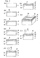
- an insulating film 2 of non-crystal is formed on a top plane of a (100) monocrystal silicon base-plate 1 under being partially exposed to provide an exposed portion la, as shown in Fig. l(b), of the monocrystal silicon base-plate 1, as shown in Fig. l(a).
- the size of the monocrystal silicon base-plate exposed portion is assumed to be 3 ⁇ m square.
- the SiO 2 film of 2 ⁇ m in thickness is formed on the monocrystal silicon base-plate 1 by means of, for example, a known thermal oxidation method.
- the monocrystal silicon base-plate 1 of the SiO 2 film is selection-etched by a known photoeching method only in the portion to be exposed to form a plurality of opening portions la, la, la, ... of dot shapes, each being 3 ⁇ m square in the interval 15 um, as shown in Fig. 2.
- a piece of non-crystalloid or multicrystal silicon thin film 3 which is almost equal in thickness to the insulating film 2, as shown in Fig. l(c), is embedded only into the exposed portion la of the monocrystal silicon base-plate 1 provided in and surrounded by the insulating film 2.
- either of the non-crystalloid silicon thin-film or multicrystal silicon thin-film is formed by a known LPCVD method on the whole surface of the insulating film 2 including the opening portion la therein.
- organic application film material is applied to paint to be even on the whole surface of the non-crystalloid or multi- crystal silicon thin-film, which is formed unevenly on the surface corresponding to the opening portion la of the monocrystal silicon base-plate 1 and the surface of the insulating film 2, to form an organic application film.
- the equal-speed etching is performed from the surface of the organic application film surface to transfer the even surface of the initial organic application film, and the etching operation is stopped in a time point when the insulating film 2 has been exposed with filling the non-crystalloid or multicrystal silicon thin-film 3 into the opening portion la of the insulating film 2, as shown in Fig. 1 (c) .
- the step difference in surface between the non-crystalloid or multicrystal silicon thin film 3 filled in at this time, and the insulating film 2 is assumed to be 1 ⁇ m or less.
- a non-crystalloid or multicrystal silicon thin film 4 which becomes an active layer of 0.6 ⁇ m in thickness is formed by the LPCVD method on both regions by the upper portion of the thin film 3 filled in and of the upper portion of the insulating film 2, as shown in Fig. l(d). Furthermore, an SiO 2 film which serves as a surface protective film, i.e., anti-reflective film 5 for the silicon thin film 4 is formed by the APCVD method into 850 A in thickness on the whole surface of the silicon thin film 4, as shown in Fig. l(e).
- a non-crystalloid or multicrystal silicon thin-film 8 of stripe-shape on the surface of the surface protective film 5, as shown in Figs. l(g) and 1(h) at the state of that longitudinal direction of the stripe may become (010) of the monocrystal silicon base plate 1, as shown in Fig. 2.
- the non-crystalloid or multi- crystal silicon thin film 8 is formed 0.6 ⁇ m in thickness by the LPCVD method on the surface protective film 5, and is made stripe-shaped through the selective etching operation by a known photo-etching method.
- each stripe of the non-crystalloid or multicrystal silicon thin film 8 is formed to cover the monocrystal silicon base-plate exposed portion la with the width of stripe being 10 ⁇ m, the internal between the stripes being 5 ⁇ m.
- the scanning operation of the laser beam 9 of 60 ⁇ m in molten width and 12 W in power is effected from the monocrystal silicon base-plate exposed portion la with the scanning speed of 100 mm per second in the longitudinal direction of the stripe-shaped non-crystalloid or multicrystal siliccn thin-film 8, as shown in Fig. l(i), to provide a monocrystal silicon thin film 10 in which the non-crystalloid or multicrystal silicon thin-film 4 is mono-crystallized with the filled silicon 7 coincided with the monocrystal silicon base-plate 1 in the crystal direction being provided as the seed.
- the monocrystal silicon thin-film 10 coincided (100) with the monocrystal silicon base-plate 1 in the crystal direction is finally obtained on the surface of the insulating film 2.
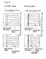
- the reason why the stripe-shaped non-crystalloid or multicrystal silicon thin-film 8 is formed is that the reflection factor, i.e., reflectivity of the laser beam 9 in the place where the stripe-shaped silicon is located is enlarged than that in the place where the stripe-shaped silicon does not exist, as shown in Fig. 3(a), the solidification for monocrystallization starts from right under the stripe-shaped silicon central portion with such temperature distribution being provided, as shown in Fig. 3(b), and the monocrystal growth of the silicon thin film 10 is caused with the monocrystal silicon base-plate exposed portion la as the seed.
- the seeding factor of the seed is changed by the insulating film 2 thickness when the size of the insulating film opening portion la is changed is examined for comparison, with a result as shown in Fig. 4.
- the opening of the opening portion la is as large as 5 ⁇ m square
- the seeding factor is lowered if the insulating film 2 becomes as thick as 4 ⁇ m.
- the seeding factor is not seen if-the thickness of the insulating 2 film is made 4 ⁇ m.
- the opening portion la will do well if it is made 4 ⁇ m square or less in size, because the thickness between the respective active layers is about 4 pm even at the largest.
- the reason why the crystal face of the (100) is used as the monocrystal silicon base-plate 1, and the laser scanning direction is made along the (010) is that the crystal defect is hardest to have in the combination of (100) and (010), and the monocrystal region may be smoothly enlarged from the seed portion.
- the length for which the monocrystal region extends from the seed portion when the laser scanning direction is varied between (010) and (011) by the use of the (100) monocrystal silicon base plate 1 is used as shown in Fig. 5. It is the most desirable from Fig. 5 that the laser scanning in the (010) direction is best.
- the superior monocrystal silicon thin-film 10 coincided with the monocrystal silicon base plate in the crystal direction is formed on the insulating film 2 even if the insulating film as thick as 4 ⁇ m is sufficiently covered between the active layers of the three-dimensional circuit element on the monocrystal silicon base plate 1.
Landscapes
- Recrystallisation Techniques (AREA)
Applications Claiming Priority (6)
| Application Number | Priority Date | Filing Date | Title |
|---|---|---|---|
| JP28543885A JPS62145721A (ja) | 1985-12-20 | 1985-12-20 | 単結晶薄膜の製造方法 |
| JP285438/85 | 1985-12-20 | ||
| JP6855486A JPS62226621A (ja) | 1986-03-28 | 1986-03-28 | 単結晶シリコン薄膜形成方法 |
| JP68554/86 | 1986-03-28 | ||
| JP22590086A JPS6381807A (ja) | 1986-09-26 | 1986-09-26 | 単結晶シリコン薄膜の製造方法 |
| JP225900/86 | 1986-09-26 |
Publications (3)
| Publication Number | Publication Date |
|---|---|
| EP0227076A2 true EP0227076A2 (de) | 1987-07-01 |
| EP0227076A3 EP0227076A3 (en) | 1989-05-24 |
| EP0227076B1 EP0227076B1 (de) | 1992-06-17 |
Family
ID=27299781
Family Applications (1)
| Application Number | Title | Priority Date | Filing Date |
|---|---|---|---|
| EP86117799A Expired - Lifetime EP0227076B1 (de) | 1985-12-20 | 1986-12-19 | Verfahren zur Herstellung einer monokristallinen dünnen Schicht |
Country Status (3)
| Country | Link |
|---|---|
| US (1) | US4801351A (de) |
| EP (1) | EP0227076B1 (de) |
| DE (1) | DE3685732T2 (de) |
Cited By (2)
| Publication number | Priority date | Publication date | Assignee | Title |
|---|---|---|---|---|
| EP0235819A3 (en) * | 1986-03-07 | 1988-07-27 | Iizuka, Kozo | Process for producing single crystal semiconductor layer and semiconductor device produced by said process |
| EP0236953A3 (en) * | 1986-03-07 | 1989-07-26 | Iizuka, Kozo | Method of manufacturing semiconductor crystalline layer |
Families Citing this family (3)
| Publication number | Priority date | Publication date | Assignee | Title |
|---|---|---|---|---|
| US4931323A (en) * | 1987-12-10 | 1990-06-05 | Texas Instruments Incorporated | Thick film copper conductor patterning by laser |
| FR2640428B1 (fr) * | 1988-12-09 | 1992-10-30 | Thomson Csf | Procede de durcissement vis-a-vis des rayonnements ionisants de composants electroniques actifs, et composants durcis de grandes dimensions |
| TW264575B (de) * | 1993-10-29 | 1995-12-01 | Handotai Energy Kenkyusho Kk |
Family Cites Families (10)
| Publication number | Priority date | Publication date | Assignee | Title |
|---|---|---|---|---|
| JPS5734331A (en) * | 1980-08-11 | 1982-02-24 | Toshiba Corp | Manufacture of semiconductor device |
| US4487639A (en) * | 1980-09-26 | 1984-12-11 | Texas Instruments Incorporated | Localized epitaxy for VLSI devices |
| US4448632A (en) * | 1981-05-25 | 1984-05-15 | Mitsubishi Denki Kabushiki Kaisha | Method of fabricating semiconductor devices |
| US4565599A (en) * | 1981-12-21 | 1986-01-21 | Massachusetts Institute Of Technology | Graphoepitaxy by encapsulation |
| JPS58130517A (ja) * | 1982-01-29 | 1983-08-04 | Hitachi Ltd | 単結晶薄膜の製造方法 |
| JPS59108313A (ja) * | 1982-12-13 | 1984-06-22 | Mitsubishi Electric Corp | 半導体単結晶層の製造方法 |
| CA1197628A (en) * | 1984-01-05 | 1985-12-03 | Thomas W. Macelwee | Fabrication of stacked mos devices |
| US4555300A (en) * | 1984-02-21 | 1985-11-26 | North American Philips Corporation | Method for producing single crystal layers on insulators |
| FR2580672B1 (fr) * | 1985-04-19 | 1987-05-15 | France Etat | Procede de fabrication sur un support isolant d'un film de silicium monocristallin oriente et a defauts localises |
| US4651407A (en) * | 1985-05-08 | 1987-03-24 | Gte Laboratories Incorporated | Method of fabricating a junction field effect transistor utilizing epitaxial overgrowth and vertical junction formation |
-
1986
- 1986-12-19 DE DE8686117799T patent/DE3685732T2/de not_active Expired - Fee Related
- 1986-12-19 US US06/943,428 patent/US4801351A/en not_active Expired - Lifetime
- 1986-12-19 EP EP86117799A patent/EP0227076B1/de not_active Expired - Lifetime
Cited By (2)
| Publication number | Priority date | Publication date | Assignee | Title |
|---|---|---|---|---|
| EP0235819A3 (en) * | 1986-03-07 | 1988-07-27 | Iizuka, Kozo | Process for producing single crystal semiconductor layer and semiconductor device produced by said process |
| EP0236953A3 (en) * | 1986-03-07 | 1989-07-26 | Iizuka, Kozo | Method of manufacturing semiconductor crystalline layer |
Also Published As
| Publication number | Publication date |
|---|---|
| EP0227076B1 (de) | 1992-06-17 |
| DE3685732T2 (de) | 1993-01-21 |
| EP0227076A3 (en) | 1989-05-24 |
| DE3685732D1 (de) | 1992-07-23 |
| US4801351A (en) | 1989-01-31 |
Similar Documents
| Publication | Publication Date | Title |
|---|---|---|
| US4596604A (en) | Method of manufacturing a multilayer semiconductor device | |
| US4523962A (en) | Method for fabricating monocrystalline semiconductor layer on insulating layer by laser crystallization using a grid of anti-reflection coating disposed on poly/amorphous semiconductor | |
| USRE33096E (en) | Semiconductor substrate | |
| EP0235819A2 (de) | Verfahren zum Herstellen einer monokristallinen Halbleiterschicht | |
| US4599133A (en) | Method of producing single-crystal silicon film | |
| EP0227076A2 (de) | Verfahren zur Herstellung einer monokristallinen dünnen Schicht | |
| JPH027415A (ja) | Soi薄膜形成方法 | |
| US5094714A (en) | Wafer structure for forming a semiconductor single crystal film | |
| GB2153253A (en) | Semiconductor device and process for making it | |
| JPS62179112A (ja) | Soi構造形成方法 | |
| JPH0442358B2 (de) | ||
| JPS58180019A (ja) | 半導体基体およびその製造方法 | |
| JPS62145721A (ja) | 単結晶薄膜の製造方法 | |
| JPS6315471A (ja) | 薄膜トランジスタとその製造方法 | |
| JPH01162322A (ja) | 半導体単結晶層の製造方法 | |
| JPH0652711B2 (ja) | 半導体装置 | |
| JPS6339554B2 (de) | ||
| JPH03250620A (ja) | 半導体装置の製造方法 | |
| JPS62250629A (ja) | 半導体装置の製造方法 | |
| JPS61240676A (ja) | 半導体薄膜結晶の製造方法 | |
| JPS5978999A (ja) | 半導体単結晶膜の製造方法 | |
| JPS62199013A (ja) | Soi膜再結晶化法 | |
| JPS61212012A (ja) | Soi構造形成方法 | |
| JPH01290219A (ja) | 半導体装置の製造方法 | |
| JPS60229330A (ja) | 半導体装置の製造方法 |
Legal Events
| Date | Code | Title | Description |
|---|---|---|---|
| PUAI | Public reference made under article 153(3) epc to a published international application that has entered the european phase |
Free format text: ORIGINAL CODE: 0009012 |
|
| 17P | Request for examination filed |
Effective date: 19861219 |
|
| AK | Designated contracting states |
Kind code of ref document: A2 Designated state(s): DE FR GB |
|
| PUAL | Search report despatched |
Free format text: ORIGINAL CODE: 0009013 |
|
| AK | Designated contracting states |
Kind code of ref document: A3 Designated state(s): DE FR GB |
|
| RHK1 | Main classification (correction) |
Ipc: H01L 21/268 |
|
| 17Q | First examination report despatched |
Effective date: 19910131 |
|
| GRAA | (expected) grant |
Free format text: ORIGINAL CODE: 0009210 |
|
| AK | Designated contracting states |
Kind code of ref document: B1 Designated state(s): DE FR GB |
|
| REF | Corresponds to: |
Ref document number: 3685732 Country of ref document: DE Date of ref document: 19920723 |
|
| ET | Fr: translation filed | ||
| PLBE | No opposition filed within time limit |
Free format text: ORIGINAL CODE: 0009261 |
|
| STAA | Information on the status of an ep patent application or granted ep patent |
Free format text: STATUS: NO OPPOSITION FILED WITHIN TIME LIMIT |
|
| 26N | No opposition filed | ||
| PGFP | Annual fee paid to national office [announced via postgrant information from national office to epo] |
Ref country code: GB Payment date: 19961210 Year of fee payment: 11 |
|
| PGFP | Annual fee paid to national office [announced via postgrant information from national office to epo] |
Ref country code: FR Payment date: 19961227 Year of fee payment: 11 Ref country code: DE Payment date: 19961227 Year of fee payment: 11 |
|
| PG25 | Lapsed in a contracting state [announced via postgrant information from national office to epo] |
Ref country code: GB Free format text: LAPSE BECAUSE OF NON-PAYMENT OF DUE FEES Effective date: 19971219 |
|
| PG25 | Lapsed in a contracting state [announced via postgrant information from national office to epo] |
Ref country code: FR Free format text: THE PATENT HAS BEEN ANNULLED BY A DECISION OF A NATIONAL AUTHORITY Effective date: 19971231 |
|
| GBPC | Gb: european patent ceased through non-payment of renewal fee |
Effective date: 19971219 |
|
| PG25 | Lapsed in a contracting state [announced via postgrant information from national office to epo] |
Ref country code: DE Free format text: LAPSE BECAUSE OF NON-PAYMENT OF DUE FEES Effective date: 19980901 |
|
| REG | Reference to a national code |
Ref country code: FR Ref legal event code: ST |