EP0227318B1 - Verschlüsselungs-/Entschlüsselungssystem - Google Patents
Verschlüsselungs-/Entschlüsselungssystem Download PDFInfo
- Publication number
- EP0227318B1 EP0227318B1 EP86309231A EP86309231A EP0227318B1 EP 0227318 B1 EP0227318 B1 EP 0227318B1 EP 86309231 A EP86309231 A EP 86309231A EP 86309231 A EP86309231 A EP 86309231A EP 0227318 B1 EP0227318 B1 EP 0227318B1
- Authority
- EP
- European Patent Office
- Prior art keywords
- signal
- random number
- frame
- bits
- memory
- Prior art date
- Legal status (The legal status is an assumption and is not a legal conclusion. Google has not performed a legal analysis and makes no representation as to the accuracy of the status listed.)
- Expired - Lifetime
Links
- 230000015654 memory Effects 0.000 claims description 86
- 238000004891 communication Methods 0.000 claims description 17
- 230000005540 biological transmission Effects 0.000 description 19
- 238000010586 diagram Methods 0.000 description 8
- IYZMXHQDXZKNCY-UHFFFAOYSA-N 1-n,1-n-diphenyl-4-n,4-n-bis[4-(n-phenylanilino)phenyl]benzene-1,4-diamine Chemical group C1=CC=CC=C1N(C=1C=CC(=CC=1)N(C=1C=CC(=CC=1)N(C=1C=CC=CC=1)C=1C=CC=CC=1)C=1C=CC(=CC=1)N(C=1C=CC=CC=1)C=1C=CC=CC=1)C1=CC=CC=C1 IYZMXHQDXZKNCY-UHFFFAOYSA-N 0.000 description 3
- 238000010276 construction Methods 0.000 description 3
- 230000000694 effects Effects 0.000 description 3
- 238000011084 recovery Methods 0.000 description 3
- 230000006870 function Effects 0.000 description 2
- 238000000034 method Methods 0.000 description 2
- 230000004044 response Effects 0.000 description 2
- 230000008859 change Effects 0.000 description 1
- 230000000295 complement effect Effects 0.000 description 1
- 238000003780 insertion Methods 0.000 description 1
- 230000037431 insertion Effects 0.000 description 1
- 230000007246 mechanism Effects 0.000 description 1
- 238000012986 modification Methods 0.000 description 1
- 230000004048 modification Effects 0.000 description 1
- 230000009467 reduction Effects 0.000 description 1
- 238000012552 review Methods 0.000 description 1
Images


Classifications
-
- H—ELECTRICITY
- H04—ELECTRIC COMMUNICATION TECHNIQUE
- H04L—TRANSMISSION OF DIGITAL INFORMATION, e.g. TELEGRAPHIC COMMUNICATION
- H04L9/00—Cryptographic mechanisms or cryptographic arrangements for secret or secure communications; Network security protocols
- H04L9/06—Cryptographic mechanisms or cryptographic arrangements for secret or secure communications; Network security protocols the encryption apparatus using shift registers or memories for block-wise or stream coding, e.g. DES systems or RC4; Hash functions; Pseudorandom sequence generators
- H04L9/065—Encryption by serially and continuously modifying data stream elements, e.g. stream cipher systems, RC4, SEAL or A5/3
- H04L9/0656—Pseudorandom key sequence combined element-for-element with data sequence, e.g. one-time-pad [OTP] or Vernam's cipher
- H04L9/0662—Pseudorandom key sequence combined element-for-element with data sequence, e.g. one-time-pad [OTP] or Vernam's cipher with particular pseudorandom sequence generator
-
- H—ELECTRICITY
- H04—ELECTRIC COMMUNICATION TECHNIQUE
- H04L—TRANSMISSION OF DIGITAL INFORMATION, e.g. TELEGRAPHIC COMMUNICATION
- H04L9/00—Cryptographic mechanisms or cryptographic arrangements for secret or secure communications; Network security protocols
- H04L9/12—Transmitting and receiving encryption devices synchronised or initially set up in a particular manner
-
- H—ELECTRICITY
- H04—ELECTRIC COMMUNICATION TECHNIQUE
- H04L—TRANSMISSION OF DIGITAL INFORMATION, e.g. TELEGRAPHIC COMMUNICATION
- H04L2209/00—Additional information or applications relating to cryptographic mechanisms or cryptographic arrangements for secret or secure communication H04L9/00
- H04L2209/12—Details relating to cryptographic hardware or logic circuitry
- H04L2209/125—Parallelization or pipelining, e.g. for accelerating processing of cryptographic operations
-
- H—ELECTRICITY
- H04—ELECTRIC COMMUNICATION TECHNIQUE
- H04L—TRANSMISSION OF DIGITAL INFORMATION, e.g. TELEGRAPHIC COMMUNICATION
- H04L2209/00—Additional information or applications relating to cryptographic mechanisms or cryptographic arrangements for secret or secure communication H04L9/00
- H04L2209/34—Encoding or coding, e.g. Huffman coding or error correction
Definitions
- This invention relates to devices for providing message secrecy and more particularly to an encryption/decryption system for insertion in a digitalized communication channel to maintain message privacy.
- Communication channels are increasingly being used to transmit highly confidential and important data and messages between and within businesses.
- the need to safeguard such data from eavesdropping and unauthorized tampering has grown correspondingly.
- One traditional protection technique is to encrypt the data at the transmitting end and decrypt it at the receiving end.
- certain conventional systems employ nonlinear encryption by storing a controlling encryption key variable at the transmitting and receiving ends and using a technique in which the encryption at a later time depends on the encrypted message at an earlier time.
- Such systems have an exceptionally high level of message secrecy.
- the encryption key variable can become rather slow in recovering from transmission errors in the received encrypted signal. Each transmission error interferes with correct decoding, causing a blackout period during which it is impossible to correctly decrypt a corresponding portion of the message. Enabling the encryption key variable to have a greater variety of possible values lengthens the blackout period.
- an object of this invention is to provide a new and improved encryption/decryption system which enables the encryption key variable to have a larger variety of possible values without greatly increasing the errors in the decoded signal reproduced at the receiving end. Yet another object is to provide such a device with a very high level of message secrecy without sacrificing relatively simple construction and moderate cost.
- an encryption/decryption system for a communication channel encrypts an input digital signal at the transmitting end and reproduces it at the receiving end.
- the transmitting end of the system has a first storage register, a first memory, a first selector device, and an encrypted signal composing device.
- the encrypted signal composing device combines a randomized coding signal with the input digital signal to form an encrypted signal segmented into frames.
- the invention uses cipher feedback.
- the first storage register stores bits of the encrypted signal and outputs them in parallel.
- the first memory receives these parallel bits as addresses and outputs corresponding random numbers.
- the first selector device selects from the random number data to form the randomized coding signal fed to the encrypted signal composing device.
- the receiving end has a second storage register, a second memory, a second selector device, and a digital signal reproducing device.
- the second storage register stores bits of the received encrypted signal and outputs them in parallel.
- the second memory receives these parallel bits as addresses and outputs corresponding random numbers. To enable decoding, the working and stored contents of the first and second memories are identical.
- the second selector device operating the same way as the first, selects from the random number data to form a decoding signal.
- the digital signal reproducing device combines the received encrypted signal with the randomized decoding signal to reproduce the input digital signal.
- FIG. 4 An example of a prior art encryption device employed in a communications transmitting system is shown in Fig. 4.
- Fig. 5 shows a complementary prior art decryption device employed in a communications receiving system.
- a digital input signal S is combined by an Exclusive OR (XOR) gate 2 with a randomized digital encoding signal Y successively output from a transmitter memory unit 1. This produces an encrypted signal Z for transmission.
- XOR Exclusive OR
- the successive bits of the encrypted digital signal Z are input for temporary storage to an M bit shift register 3 as shift register bits R1, R2, ..., R M .
- Memory unit 1 has 2 M addresses, each of which contains a prestored random bit, a logical 0 or 1.
- the register bits R1, R2, ..., R M are then used in parallel as an input address to memory unit 1, which outputs the prestored random bit at that address as the next bit of Y.
- the encrypted digital signal Z is input to a transmitter 4, which transmits it whenever a transmission switch 5 is closed.
- a received digital signal Z' is output by a receiver 9.
- the received signal Z' is input to an M bit shift register 6 as shift register bits R'1, R'2, ..., R' M .
- a receiver memory unit 7 has 2 M addresses, each of which contains a prestored bit.
- the register bits R'1, R'2, ..., R' M are then used in parallel as an input address to memory unit 7, which outputs the prestored random bit at that address as the next bit of a decoding signal Y'.
- the received signal Z' is successively combined by an Exclusive OR (XOR) gate 8 with the decoding signal Y' to generate a reproduced signal S'.
- XOR Exclusive OR
- the prestored random bits of the receiver memory unit 7 of the receiving system are made identical to those stored in the corresponding addresses of the transmitter memory unit 1 of the transmitting system.
- Z' Z
- the encryption and decryption operations are controlled by the particular random bit pattern stored in the addresses in memory units 1 and 6. This important controlling bit pattern is called the encryption key variable.
- Such conventional encryption/decryption devices have the advantages of simple construction and, because they use nonlinear encryption, an exceptionally high level of message secrecy.
- they have the disadvantage that increasing the number of possible random bit patterns that might be stored in the memories 1 and 7, that is enabling the encryption key variable to have a larger variety of possible values, also increases the system's weakness with respect to transmission errors.
- increasing the number of possible random bit patterns that might be stored in the memories 1 and 7, that is enabling the encryption key variable to have a larger variety of possible values also increases the system's weakness with respect to transmission errors.
- the number of bits M used in shift registers 3 and 6 must be increased to add more addresses.
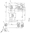
- Fig. 1 shows a block diagram of a first embodiment of an encryption system that overcomes these problems for use at the transmitting end of a communications link.
- An XOR (Exclusive OR) gate 10 combines an input digital signal S with a randomized coding signal Y to produce an encrypted digital signal Z.
- a shift register 12 receives and temporarily stores the successive bits of signal Z as register bits r1, r2, ..., r m .
- the m register bits are then provided in parallel as an input memory address to a transmitter memory unit 22.
- Each of the 2 m addresses in memory unit 22 is prestored with a corresponding n bit random number x1, x2, ..., x n .
- the number n is an integer equal to or greater than 2.
- encoder memory 22 outputs its corresponding stored random number x1, x2, ..., x n .
- Random selection circuit 11 selects from among the n bit random number data x1, x2, ..., x n output by memory unit 22 to form each frame of bits of the coding signal Y.
- Random selection circuit 11 comprises an encoder frame counter 15, an encoder memory 14, and an encoder selector circuit 13.
- a frame pulse FP output by a frame sync pulse generator 16 is input as a clock signal to counter 15, which has q bits.
- the counter bits b1, b2, ..., b q are provided in parallel as an input memory address to the encoder memory 14.
- Each of the 2 q addresses in encoder memory 14 is prestored with a corresponding p bit random number a1, a2, ..., a p .
- the random number a1, a2, ..., a p stored at address b1, b2, ..., b q is output to selector circuit 13 to change its selection contents.
- encoder counter 15 and encoder memory 14 together form a random number generator, generating a random number for the selector circuit 13 for each frame of the signal.
- a PN pseudo-noise
- PN pseudo-noise
- Encoding circuit 13 receives each of the n bit random numbers x1, x2, ..., x n output by transmitter memory unit 22. Based on the value of random number a1, a2, ..., a p for the current frame, random selection circuit 13 selects from among the n bit random number data x1, x2, ..., x n output by memory unit 22 to form each frame of bits of the coding signal Y. Signal Y is then combined with input signal S by XOR gate 10 to produce the encrypted digital signal Z.
- the encrypted signal Z is input to a frame composing circuit 19, which combines it with a frame sync signal FS and a START signal prefix to produce a TDATA signal for transmission.
- the frame sync signal FS is generated by a frame sync signal generator 17 in response to a frame sync pulse FP from pulse generator 16.
- the START signal prefix is generated by a start signal generator 18 in response to the closing of a transmission switch 21.
- the TDATA signal is then transmitted by a transmitter 20.
- Transmission switch 21 is arranged so that, when it is closed, it activates transmitter 20. When switch 21 is first closed, it also sends encoder counter 15 a Clear signal to set it to a preselected initial value.
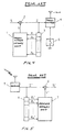
- Figure 3 shows the make-up of each frame of the TDATA signal output as well as its relationship in time to its corresponding frame sync pulse.
- "START” indicates the START signal
- "FS” the frame sync signal
- "Z” the encrypted signal Z
- "FP" the frame sync pulse.
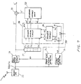
- Figure 2 shows a block diagram of a first embodiment of a decryption system for receiving the signal transmitted by the system of Fig. 1 and reproducing from it the input digital signal S.
- a receiver 23 picks up the transmitted signal of Fig. 3 and outputs a received digital signal RDATA.
- Signal RDATA is input to a separator circuit 24, a frame sync signal detector 25, and start signal detector 26.
- Separator circuit 24 separates out a received encrypted signal Z' from the received signal RDATA. If there have been no errors in the transmission path, this signal Z' is identical to the transmitted encrypted digital signal Z.
- detector 26 detects the START signal prefix at the beginning of the RDATA signal and outputs a start pulse SP.
- Frame sync signal detector 25 detects each frame signal FS and outputs a frame sync pulse FP.
- the frame pulses FP output by detector 25 are used to synchronize separating circuit 24 so that for each frame it can separate out just the signal Z' which corresponds to the Z portion of the transmitted signal of Fig. 3.
- the frame pulse FP is also provided as a clock signal to a decoder frame counter 31 in a decoder random selection circuit 28.
- the start pulse SP from detector 26 is provided as a Clear signal to counter 31 to set it to a preselected initial value.
- the encrypted received signal Z' output by circuit 24 is input to both a shift register 27 and an XOR gate 33.
- Shift register 27 receives and temporarily stores the successive bits of signal Z' as register bits r'1, r'2, ..., r' m . These m register bits are then provided in parallel as an input memory address to a receiver memory unit 32.
- Each of the 2 m addresses in memory unit 32 is prestored with a corresponding n bit random number x'1, x'2, ..., x' n .
- the random number x'1, x'2, ..., x' n stored at that address is output.
- a decoder selector circuit 29 in random selection circuit 28 receives and selects from among the n bit random number data x'1, x'2, ..., x' n output by memory unit 32 to form each frame of bits of a decoding signal Y'.
- Signal Y' is then provided to the XOR gate 33.
- Decoder random selection circuit 28 works exactly like the encoder random selection circuit 11 in the encryption system at the transmitting end.
- Decoder counter 31 is initialized by a start pulse SP from detector 26 before counting the frame sync pulses FP output by detector 25.
- the output b'1, b'2, ..., b' q of counter 31 is provided in parallel as address input to a decoder memory 30 for each frame. This outputs a stored random number a'1, a'2, ..., a' p for each address.
- the random number output a'1, a'2, ..., a' p controls the selection contents of decoder selector circuit 29 for each frame.
- random selection circuit 29 selects from among the n bit random number data x'1, x'2, ..., x' n output by memory unit 32 to form each frame of bits of the decoding signal Y' for XOR gate 33.
- the XOR gate 33 then combines encrypted received signal Z' with decoding signal Y' to reproduce digital signal S' as the decrypted message signal.
- Counter 15 at the transmitting end and counter 31 at the receiving end are each set to the same preselected initial value before they begin counting frame sync pulses.
- Decoder memory 30 is prestored with the same pattern of random numbers prestored in encoder memory 14. This enables decoder random selection circuit 28 to follow the identical selection routine employed by encoder random selection circuit 11.
- Receiver memory unit 32 is prestored with the same pattern of random numbers prestored in transmitter memory unit 22. Therefore, when there are no transmission errors, the reproduced digital signal S' at the receiver end is identical to the digital signal S input at the transmitting end. For no transmission errors, this result is just as in the prior art encoder/decoder system.
- the logical working of the decoding mechanism is as follows. When no errors are introduced by the transmission path, the received signal Z' equals the encrypted cipher signal Z. Then shift registers 27 and 12 provide the same address inputs to memory units 32 and 22, having identical contents. Each random number x'1, x'2, ..., x' n output by receiver memory unit 32 is identical to the random number x1, x2, ..., x n previously output by transmitter memory unit 22.
- decoder random selection circuit 28 can duplicate the working of encoder random selection circuit 11. This enables randomized signal Y' to be identical to randomized signal Y.
- shift registers 12, 27 to have only m bits, where m is less than the usual M bits used in prior art shift registers 3 and 6 of Figs. 4 and 5. If an error is generated in the transmission path, it causes errors in the decoding signal Y' for a time interval equal to the time it takes to transmit m bits. However, because the number of bits m in register 27 can be less than the usual M bits, the amount of time that the received signal S' is not properly reproduced is reduced.
- the number of bits n stored at each memory address can be selected to be a relatively small number as compared to the address length m, reducing the complexity of encoder selector circuit 13 and decoder selector circuit 29.
- the variety of random numbers stored in the encoder memory 14 and decoder memory 30 can be made very large. This effectively gives the encryption key variable a large number of possible values without increasing the errors in decoding signal Y' or the reproduced digital signal S'.
- the present invention not only randomizes individual signal bits in the transmitted signal but also changes the selection rule used by encoder random selection circuit 11 to form encoding signal Y for each frame of the message. This ensures an exceptionally strong level of message secrecy without greatly increasing the errors in reproduced digital signal S'. The number of different values for the encryption key variable of the coder/encoder is greatly increased without sacrificing the system's prompt recovery from any transmission channel errors.
- a cipher feedback loop comprising, in order, a register (12), a transmitter memory unit (22), and a random selection circuit (11) provides the randomized coding signal Y.
- the decoding signal Y' is provided by a cipher feedback loop comprising, in order, a register (27), a transmitter memory unit (32), and a random selection circuit (28).
- Fig. 6 shows a second embodiment of the inventive encryption system having a different cipher feedback loop comprising, in order, a shift register 12, a random selection circuit 41, and a transmitter memory unit 42.
- the remaining portions of the second embodiment of the encryption system are identical to those shown in Fig. 1 for the first embodiment, as indicated by use of identical reference numerals.
- shift register 12 stores and outputs in parallel a predetermined number of bits m of the encrypted signal Z output from the XOR gate 10. For each signal frame, random selection circuit 41 randomly selects from among the m bit number data output by shift register 12 and outputs corresponding n bit address numbers w1, w2, ..., w n , where n is an integer equal to or greater than 2.
- Transmitter memory unit 42 receives the n bit addresses and for each address w1, w2, ..., w n outputs a corresponding random bit prestored at the address. The successive bits output by memory unit 42 make up the randomized coding signal Y.
- Random selection circuit 41 has a frame counter 45 fed by frame sync pulses FP from a frame sync pulse generator 16.
- the output of frame counter 45 is a q bit number b1, b2 ..., b q for each frame.
- An encoder memory 44 receives the q bit output of counter 45 as an address. It outputs a p bit random number a1, a2, ..., a p prestored at that address to a selector circuit 43 which executes the selection made by selection circuit 41.
- the selection rule of selector circuit 43 is controlled by the value of random number a1, a2, ..., a p for the current frame. In effect, counter 45 and encoder memory 44 generate a p bit random number a1, a2, ..., a p for each frame for controlling selector circuit 43.
- Fig. 7 shows a second embodiment of the inventive decryption system for use at the receiving end of a communications link to decode signals transmitted by the system of Fig. 6.
- This decryption system has a cipher feedback loop comprising, in order, a shift register 27, a random selection circuit 58, and a receiver memory unit 52.
- the remaining portions of the second embodiment of the decryption system are identical to those shown in Fig. 2 for the first embodiment, as indicated by use of identical numerals.
- shift register 27 stores and outputs in parallel a predetermined number of bits m of the received encrypted signal Z' output from separating circuit 24.
- the selection circuit 58 selects from among the m bit number data output by shift register 27 and outputs corresponding n bit address numbers w'1, w'2, ..., w' n .
- Receiver memory unit 52 has stored contents identical to that of transmitter memory unit 42 (Fig. 6). Memory unit 52 receives the n bit addresses and for each address w'1, w'2, ..., w' n outputs a corresponding random bit (0 or 1) prestored at the address. The successive bits output by memory unit 52 make up the decoding signal Y'.
- Selection circuit 58 operates the same way as random selection circuit 41 and in sync with a corresponding frame of the encrypted signal Z.
- Circuit 58 has a frame counter 51 fed by frame sync pulses from a frame sync signal detector 25.
- the output of frame counter 51 is a q bit number b'1, b'2 ..., b' q for each frame.
- a decoder memory 50 has stored contents identical to that of encoder memory 44 (Fig. 6).
- Decoder memory 50 receives the q bit output of counter 51 as an address. It outputs a p bit number a'1, a'2, ..., a' p prestored at that address to a selector circuit 59 which executes the selection made by selection circuit 58.
- the selection rule of selector circuit 59 is controlled by the value of random number a'1, a'2, ..., a' p for the current frame.
- counter 51 and decoder memory 50 generate a p bit number a'1, a'2 .., a' p for each frame for controlling selector circuit 59.
- the remaining portions of the second embodiment of the decryption system function like those shown in Fig. 2 for the first embodiment, their working will not again be described.
- the stored contents and working of the decryption system are chosen to replicate those of the encryption system.
- the received encrypted signal Z' equals the encrypted signal Z
- the decoding signal Y' equals the randomized encoding signal Y.
- the second embodiment of the encryption and decryption systems enables the number of values for the encryption key variable to be increased without increasing the number of bits m used in the shift registers 12 and 27. Instead, the additional randomizing key information is provided in the encrypter by the working of selector circuit 43, transmitter memory 42, encoder memory 44, and frame counter 45, and their counterparts in the decryption system.
- the number of bits n in address numbers w1, w2, ..., w n and w'1, w'2, ..., w' n can be selected to be a relatively small number as compared to the address length m, reducing the complexity of transmitter memory unit 42 and receiver memory unit 52.
- an address may be incremented by means of frame sync signals, the intervals between which may constitute an information data word.
Landscapes
- Engineering & Computer Science (AREA)
- Computer Security & Cryptography (AREA)
- Computer Networks & Wireless Communication (AREA)
- Signal Processing (AREA)
- Transmission Systems Not Characterized By The Medium Used For Transmission (AREA)
- Mobile Radio Communication Systems (AREA)
- Two-Way Televisions, Distribution Of Moving Picture Or The Like (AREA)
- Time-Division Multiplex Systems (AREA)
Claims (2)
- Verschlüsselungs-/Entschlüsselungssystem zum Verschlüsseln eines auf der Sendeseite eines Kommunikationskanals eingegebenen Digitalsignals und zum Reproduzieren des Eingabesignals auf der Empfangsseite des Kanals, das aufweist: auf der Sendeseite ein erstes Register (12) zum Speichern einer vorbestimmten Bitanzahl m eines verschlüsselten Signals und zum parallelen Ausgeben mehrerer der gespeicherten Bits, einen ersten Speicher (22) zum Empfangen der Ausgabe von dem ersten Register (12) als Adreßeingabe und zum Ausgeben einer entsprechenden vorgespeicherten n-Bit-Zufallszahl für jede der verschiedenen Eingabeadressen und eine Einrichtung (11) zum Erzeugen eines Zufallscodiersignals, das mit dem digitalen Eingabesignal zu einem verschlüsselten Signal zu kombinieren ist, um ein verschlüsseltes Signal zu bilden, und auf der Empfangsseite einen zweiten Registerspeicher (32) zum Empfangen der Ausgabe von einem zweiten Register (27) als Adreßeingabe und zum Ausgeben einer entsprechenden vorgespeicherten n-Bit-Zufallszahl für jede der verschiedenen Eingabeadressen, wobei der gespeicherte Inhalt des ersten (22) und zweiten (32) Speichers identisch ist, und eine Einrichtung (33) zum Kombinieren des verschlüsselten Empfangssignals mit einem Decodiersignal, um das auf der Sendeseite eingegebene Digitalsignal zu reproduzieren,
dadurch gekennzeichnet, daß
auf der Sendeseite die Erzeugungseinrichtung (11) aufweist: einen ersten Zufallszahlengenerator (14, 15, 16) zum lokalen Erzeugen einer ersten Zufallszahl für jeden Rahmen und eine erste Auswahleinrichtung (13) zum zufälligen Auswählen einer Ausgabe aus den durch den ersten Speicher (22) ausgegebenen n-Bit-Zufallszahlendaten auf der Grundlage der ersten Zufallszahl von dem ersten Zufallszahlengenerator (14, 15, 16), wobei n gleich 2 oder eine größere Ganzzahl ist, um jeden Bitrahmen des Zufallscodiersignals zu bilden, und daß auf der Empfangsseite vorgesehen sind: ein zweiter Zufallszahlengenerator (25, 30, 31) zum lokalen Erzeugen einer zweiten Zufallszahl für jeden Rahmen synchron zu einem entsprechenden Rahmen des verschlüsselten Signals und eine auf ähnliche Weise wie die erste Auswahleinrichtung (13) arbeitende zweite Auswahleinrichtung (29) zum Auswählen einer Ausgabe aus den von dem zweiten Speicher (32) ausgegebenen Zufallszahlendaten auf der Grundlage der zweiten Zufallszahl von dem zweiten Zufallszahlengenerator (25, 30, 31), um das Decodiersignal durch Bilden eines Bitrahmens synchron zu einem entsprechenden Rahmen des verschlüsselten Signals vorzusehen. - Verschlüsselungs-/Entschlüsselungssystem zum Verschlüsseln eines auf der Sendeseite eines Kommunikationskanals eingegebenen Digitalsignals und zum Reproduzieren des Eingabesignals auf der Empfangsseite des Kanals, wobei das System aufweist: auf der Sendeseite ein erstes Register (12) zum Speichern einer vorbestimmten Bitanzahl m eines verschlüsselten Signals und zum parallelen Ausgeben mehrerer der gespeicherten Bits, einen ersten Speicher (42) zum Speichern und Ausgeben der Bits eines Zufallscodiersignals als Reaktion auf den Empfang einer n-Bit-Adreßzahl und eine Einrichtung (10) zum Kombinieren des Zufallscodiersignals mit dem digitalen Eingabesignal, um ein verschlüsseltes Signal zu bilden, und auf der Empfangsseite ein zweites Register (27) zum Speichern von m Bits eines verschlüsselten Empfangssignals und zum parallelen Ausgeben mehrerer der gespeicherten Bits, einen zweiten Speicher (52) mit einem darin gespeicherten Inhalt, der mit dem in dem ersten Speicher (42) gespeicherten Inhalt identisch ist, und eine Einrichtung (33) zum Kombinieren des verschlüsselten Empfangssignals mit dem Decodiersignal, um das digitale Eingabesignal zu reproduzieren,
dadurch gekennzeichnet, daß
vorgesehen sind: auf der Sendeseite ein erster Zufallszahlengenerator (16, 44, 45) zum lokalen Erzeugen einer ersten Zufallszahl für jeden Rahmen und eine erste Auswahleinrichtung (43) zum zufälligen Auswählen einer Ausgabe für jeden Signalrahmen auf der Grundlage der ersten Zufallszahl von dem ersten Zufallszahlengenerator (16, 44, 45) und als Reaktion auf die durch das erste Register (12) ausgegebenen m-Bit-Zahlendaten und zum Ausgeben der n-Bit-Adreßzahl, wobei n gleich 2 oder eine größere Ganzzahl ist, und auf der Empfangsseite ein zweiter Zufallszahlengenerator (25, 50, 51) zum lokalen Erzeugen einer zweiten Zufallszahl für jeden Rahmen synchron zu einem entsprechenden Rahmen des verschlüsselten Signals und eine auf ähnliche Weise wie die erste Auswahleinrichtung (43) und synchron zu dem entsprechenden Rahmen des verschlüsselten Signals arbeitende zweite Auswahleinrichtung (59) zum Auswählen einer Ausgabe auf der Grundlage der zweiten Zufallszahl von dem zweiten Zufallszahlengenerator (25, 50, 51) und als Reaktion auf die durch das zweite Register (27) ausgegebenen m-Bit-Zahlendaten und Ausgeben entsprechender n-Bit-Adreßzahlen, wobei der zweite Speicher (52) ein vorgespeichertes Decodiersignal als Reaktion auf den Empfang der von der zweiten Auswahleinrichtung (59) ausgegebenen n-Bit-Adressen erzeugt.
Applications Claiming Priority (4)
| Application Number | Priority Date | Filing Date | Title |
|---|---|---|---|
| JP268322/85 | 1985-11-30 | ||
| JP268321/85 | 1985-11-30 | ||
| JP60268322A JPH0630495B2 (ja) | 1985-11-30 | 1985-11-30 | 暗号化装置 |
| JP60268321A JPH0628354B2 (ja) | 1985-11-30 | 1985-11-30 | 暗号化装置 |
Publications (3)
| Publication Number | Publication Date |
|---|---|
| EP0227318A2 EP0227318A2 (de) | 1987-07-01 |
| EP0227318A3 EP0227318A3 (en) | 1989-02-22 |
| EP0227318B1 true EP0227318B1 (de) | 1993-07-07 |
Family
ID=26548266
Family Applications (1)
| Application Number | Title | Priority Date | Filing Date |
|---|---|---|---|
| EP86309231A Expired - Lifetime EP0227318B1 (de) | 1985-11-30 | 1986-11-26 | Verschlüsselungs-/Entschlüsselungssystem |
Country Status (5)
| Country | Link |
|---|---|
| US (1) | US4791669A (de) |
| EP (1) | EP0227318B1 (de) |
| AU (1) | AU589080B2 (de) |
| CA (1) | CA1258305A (de) |
| DE (1) | DE3688676T2 (de) |
Cited By (1)
| Publication number | Priority date | Publication date | Assignee | Title |
|---|---|---|---|---|
| RU2502201C2 (ru) * | 2006-09-01 | 2013-12-20 | Сони Корпорейшн | Устройство обработки шифрования/дешифрования, способ обработки шифрования/дешифрования, устройство обработки информации и компьютерная программа |
Families Citing this family (36)
| Publication number | Priority date | Publication date | Assignee | Title |
|---|---|---|---|---|
| US5261070A (en) * | 1986-07-24 | 1993-11-09 | Meiji Milk Product Co., Ltd. | Method and apparatus for forming unique user identification data at remote terminal for secure transmission of data from host terminal |
| US4969188A (en) * | 1987-02-17 | 1990-11-06 | Gretag Aktiengesellschaft | Process and apparatus for the protection of secret elements in a network of encrypting devices with open key management |
| US5113444A (en) * | 1990-09-05 | 1992-05-12 | Arnold Vobach | Random choice cipher system and method |
| JP2862030B2 (ja) * | 1991-06-13 | 1999-02-24 | 三菱電機株式会社 | 暗号化方式 |
| US5199074A (en) * | 1992-01-06 | 1993-03-30 | Advanced Micro Devices, Inc. | Encryption system |
| US5307412A (en) * | 1992-09-30 | 1994-04-26 | Vobach Arnold R | Random coding cipher system and method |
| US5335280A (en) * | 1993-01-28 | 1994-08-02 | Vobach Arnold R | Random sum cipher system and method |
| NL9400428A (nl) * | 1994-03-18 | 1995-11-01 | Nederland Ptt | Inrichting voor het cryptografisch bewerken van datapakketten, alsmede werkwijze voor het genereren van cryptografische bewerkingsdata. |
| SE506619C2 (sv) * | 1995-09-27 | 1998-01-19 | Ericsson Telefon Ab L M | Metod för kryptering av information |
| US5859912A (en) * | 1996-03-22 | 1999-01-12 | General Electric Company | Digital information privacy system |
| JPH10301492A (ja) | 1997-04-23 | 1998-11-13 | Sony Corp | 暗号化装置および方法、復号装置および方法、並びに情報処理装置および方法 |
| JP4456185B2 (ja) * | 1997-08-29 | 2010-04-28 | 富士通株式会社 | コピー防止機能を持つ見える透かし入り動画像記録媒体とその作成・検出および録画・再生装置 |
| ES2548860T3 (es) * | 2000-01-14 | 2015-10-21 | Mitsubishi Denki Kabushiki Kaisha | Codificador, procedimiento de codificación, decodificador, procedimiento de decodificación y medio de grabación legible por ordenador que tiene almacenado un programa en el mismo |
| US6931128B2 (en) * | 2001-01-16 | 2005-08-16 | Microsoft Corporation | Methods and systems for generating encryption keys using random bit generators |
| US8121292B2 (en) * | 2002-02-26 | 2012-02-21 | Qualcomm Incorporated | Method and apparatus for scrambling information bits on a channel in a communications system |
| JP4199477B2 (ja) * | 2002-04-17 | 2008-12-17 | パナソニック株式会社 | デジタル双方向通信制御装置およびその方法 |
| JP3661663B2 (ja) * | 2002-04-19 | 2005-06-15 | 日本電気株式会社 | 乱数生成装置、乱数生成方法、乱数生成プログラムおよびオーディオ復号装置と復号方法 |
| US20040025039A1 (en) * | 2002-04-30 | 2004-02-05 | Adam Kuenzi | Lock box security system with improved communication |
| US7061367B2 (en) | 2002-04-30 | 2006-06-13 | General Electric Company | Managing access to physical assets |
| KR20050032588A (ko) * | 2002-08-08 | 2005-04-07 | 마츠시타 덴끼 산교 가부시키가이샤 | 암호화 복호화장치 및 방법, 암호화장치 및 방법,복호화장치 및 방법, 그리고 송수신장치 |
| US8171567B1 (en) | 2002-09-04 | 2012-05-01 | Tracer Detection Technology Corp. | Authentication method and system |
| CN100428666C (zh) * | 2002-12-16 | 2008-10-22 | 中国电子科技集团公司第三十研究所 | 一种密码芯片密钥快速更换方法 |
| AU2005220385B2 (en) * | 2004-03-12 | 2010-07-15 | Ingenia Holdings Limited | Authenticity verification methods, products and apparatuses |
| DE602005014755D1 (de) | 2004-03-12 | 2009-07-16 | Ingenia Technology Ltd | Verfahren und vorrichtungen zur erzeugung authentifizierbarer gegenstände und ihrer nachfolgenden überprüfung |
| JP2006023957A (ja) * | 2004-07-07 | 2006-01-26 | Sony Corp | 半導体集積回路及び情報処理装置 |
| GB2417592B (en) | 2004-08-13 | 2006-07-26 | Ingenia Technology Ltd | Authenticity verification of articles |
| GB2438424B (en) * | 2004-08-13 | 2008-02-13 | Ingenia Technology Ltd | Article manufacturing screen |
| US7458008B2 (en) * | 2004-12-30 | 2008-11-25 | Freescale Semiconductor, Inc. | Decision voting in a parallel decoder |
| US7764792B1 (en) * | 2005-01-13 | 2010-07-27 | Marvell International Ltd. | System and method for encoding data transmitted on a bus |
| RU2417448C2 (ru) * | 2005-07-27 | 2011-04-27 | Инджениа Холдингс Лимитед | Верификация аутентичности |
| CN101923647B (zh) | 2005-12-23 | 2013-01-09 | 英根亚控股有限公司 | 光学鉴别 |
| US9670694B2 (en) | 2007-04-12 | 2017-06-06 | Utc Fire & Security Americas Corporation, Inc. | Restricted range lockbox, access device and methods |
| US8233622B2 (en) * | 2008-06-18 | 2012-07-31 | International Business Machines Corporation | Transmitting parallel data via high-speed serial interconnection |
| GB2466311B (en) | 2008-12-19 | 2010-11-03 | Ingenia Holdings | Self-calibration of a matching algorithm for determining authenticity |
| GB2466465B (en) | 2008-12-19 | 2011-02-16 | Ingenia Holdings | Authentication |
| GB2476226B (en) | 2009-11-10 | 2012-03-28 | Ingenia Holdings Ltd | Optimisation |
Family Cites Families (20)
| Publication number | Priority date | Publication date | Assignee | Title |
|---|---|---|---|---|
| US3614316A (en) * | 1964-05-20 | 1971-10-19 | Us Navy | Secure communication system |
| CH411030A (de) * | 1964-08-06 | 1966-04-15 | Patelhold Patentverwertung | Einrichtung zur Verschlüsselung einer impulsförmigen Nachricht |
| CH516854A (de) * | 1969-11-29 | 1971-12-15 | Ciba Geigy Ag | Verfahren und Vorrichtung zur chiffrierten Übermittlung von Informationen |
| CH530742A (de) * | 1970-08-24 | 1972-11-15 | Ciba Geigy Ag | Vorrichtung zur Erzeugung von Schlüsselimpulsfolgen |
| US3852534A (en) * | 1973-06-07 | 1974-12-03 | Us Army | Method and apparatus for synchronizing pseudorandom coded data sequences |
| US4176247A (en) * | 1973-10-10 | 1979-11-27 | Sperry Rand Corporation | Signal scrambler-unscrambler for binary coded transmission system |
| SE380696B (sv) * | 1974-03-20 | 1975-11-10 | Philips Svenska Ab | Sett att alstra en pseudoslumpbitfoljd och anordning for utforande av settet. |
| SE385644B (sv) * | 1974-10-17 | 1976-07-12 | Ericsson Telefon Ab L M | Anordning vid kryptering och dekryptering av meddelanden |
| US3950616A (en) * | 1975-04-08 | 1976-04-13 | Bell Telephone Laboratories, Incorporated | Alignment of bytes in a digital data bit stream |
| US4133974A (en) * | 1976-11-05 | 1979-01-09 | Datotek, Inc. | System for locally enciphering prime data |
| DE2706421C2 (de) * | 1977-02-16 | 1979-03-15 | Licentia Patent-Verwaltungs-Gmbh, 6000 Frankfurt | Verfahren zum Einstellen von Schlüsseltextgeneratoren in Chiffriergeräten |
| US4172213A (en) * | 1977-11-17 | 1979-10-23 | Burroughs Corporation | Byte stream selective encryption/decryption device |
| JPS54129901A (en) * | 1978-03-31 | 1979-10-08 | Toshiba Corp | Secret communication system |
| NL183862C (nl) * | 1980-02-04 | 1989-02-01 | Philips Nv | Telecommunicatiestelsel met gecodeerde berichtoverdracht. |
| US4447672A (en) * | 1980-10-06 | 1984-05-08 | Nippon Electric Co., Ltd. | Device for encrypting each input data bit by at least one keying bit decided by a code pattern and a bit pattern of a predetermined number of preceding encrypted bits |
| US4450321A (en) * | 1981-12-08 | 1984-05-22 | Quigley William D | Circuit for producing noise generation for sound masking |
| GB2151886A (en) * | 1983-12-21 | 1985-07-24 | British Broadcasting Corp | Conditional-access broadcast transmission |
| EP0152251A3 (de) * | 1984-02-07 | 1986-07-30 | Communications Patents Limited | Rundfunksystem |
| US4596898A (en) * | 1984-03-14 | 1986-06-24 | Computer Security Systems, Inc. | Method and apparatus for protecting stored and transmitted data from compromise or interception |
| AU580769B2 (en) * | 1984-05-05 | 1989-02-02 | British Encryption Technology Limited | Communications system |
-
1986
- 1986-11-24 US US06/934,408 patent/US4791669A/en not_active Expired - Lifetime
- 1986-11-26 EP EP86309231A patent/EP0227318B1/de not_active Expired - Lifetime
- 1986-11-26 DE DE86309231T patent/DE3688676T2/de not_active Expired - Fee Related
- 1986-11-27 CA CA000523939A patent/CA1258305A/en not_active Expired
- 1986-11-28 AU AU65808/86A patent/AU589080B2/en not_active Ceased
Cited By (1)
| Publication number | Priority date | Publication date | Assignee | Title |
|---|---|---|---|---|
| RU2502201C2 (ru) * | 2006-09-01 | 2013-12-20 | Сони Корпорейшн | Устройство обработки шифрования/дешифрования, способ обработки шифрования/дешифрования, устройство обработки информации и компьютерная программа |
Also Published As
| Publication number | Publication date |
|---|---|
| AU589080B2 (en) | 1989-09-28 |
| CA1258305A (en) | 1989-08-08 |
| EP0227318A2 (de) | 1987-07-01 |
| DE3688676D1 (de) | 1993-08-12 |
| EP0227318A3 (en) | 1989-02-22 |
| US4791669A (en) | 1988-12-13 |
| DE3688676T2 (de) | 1993-11-04 |
| AU6580886A (en) | 1987-06-04 |
Similar Documents
| Publication | Publication Date | Title |
|---|---|---|
| EP0227318B1 (de) | Verschlüsselungs-/Entschlüsselungssystem | |
| US5193115A (en) | Pseudo-random choice cipher and method | |
| US5253294A (en) | Secure transmission system | |
| US5363447A (en) | Method for loading encryption keys into secure transmission devices | |
| US4211891A (en) | Method for setting code text generators in ciphering devices | |
| US6069954A (en) | Cryptographic data integrity with serial bit processing and pseudo-random generators | |
| US6014446A (en) | Apparatus for providing improved encryption protection in a communication system | |
| US5703948A (en) | Protected communication method and system | |
| EP1094634B1 (de) | Automatische Neusynchronisation einer Geiheimsynchronisationsinformation | |
| US5444781A (en) | Method and apparatus for decryption using cache storage | |
| KR20020016620A (ko) | 정보 암호화 방법 및 이 방법을 실현하는 장치 | |
| US5335280A (en) | Random sum cipher system and method | |
| EP0484862B1 (de) | Einrichtung zur geschützten Kommunikation und System zur geschützten Übertragung | |
| DK170266B1 (da) | Chifreringssystem og fremgangsmåde til chifrering og dechifrering | |
| US4856063A (en) | No-overhead synchronization for cryptographic systems | |
| KR100797106B1 (ko) | 무선랜에서 송수신되는 패킷의 암호화 및 복호화 방법 | |
| US4724541A (en) | Data-dependent binary encoder/decoder | |
| EP0148263A4 (de) | Wahrscheinlichkeitsverwürfler und verfahren zur wahrscheinlichtkeitsverwürflung. | |
| JP2003032244A (ja) | ストリーム暗号装置 | |
| KR100226867B1 (ko) | 무선 통신의 스트림 암호 시스템 | |
| JPH04335730A (ja) | 暗号送信装置、暗号受信装置、暗号通信システム | |
| EP0619659A2 (de) | Sequenzschrumpfgenerator für Kryptosysteme | |
| EP0035048A1 (de) | Verschlüsselungssystem, das eine veränderliche Schlüsselmatrix verwendet | |
| KR0176080B1 (ko) | 디지털 방송을 위한 가입자 제한 수신용 데이타 암호화 방법 | |
| JPS63308432A (ja) | 系列生成方法 |
Legal Events
| Date | Code | Title | Description |
|---|---|---|---|
| PUAI | Public reference made under article 153(3) epc to a published international application that has entered the european phase |
Free format text: ORIGINAL CODE: 0009012 |
|
| 17P | Request for examination filed |
Effective date: 19861219 |
|
| AK | Designated contracting states |
Kind code of ref document: A2 Designated state(s): DE FR GB NL SE |
|
| PUAL | Search report despatched |
Free format text: ORIGINAL CODE: 0009013 |
|
| AK | Designated contracting states |
Kind code of ref document: A3 Designated state(s): DE FR GB NL SE |
|
| 17Q | First examination report despatched |
Effective date: 19910423 |
|
| GRAA | (expected) grant |
Free format text: ORIGINAL CODE: 0009210 |
|
| AK | Designated contracting states |
Kind code of ref document: B1 Designated state(s): DE FR GB NL SE |
|
| PG25 | Lapsed in a contracting state [announced via postgrant information from national office to epo] |
Ref country code: NL Effective date: 19930707 |
|
| REF | Corresponds to: |
Ref document number: 3688676 Country of ref document: DE Date of ref document: 19930812 |
|
| ET | Fr: translation filed | ||
| NLV1 | Nl: lapsed or annulled due to failure to fulfill the requirements of art. 29p and 29m of the patents act | ||
| PLBE | No opposition filed within time limit |
Free format text: ORIGINAL CODE: 0009261 |
|
| STAA | Information on the status of an ep patent application or granted ep patent |
Free format text: STATUS: NO OPPOSITION FILED WITHIN TIME LIMIT |
|
| 26N | No opposition filed | ||
| EAL | Se: european patent in force in sweden |
Ref document number: 86309231.8 |
|
| PGFP | Annual fee paid to national office [announced via postgrant information from national office to epo] |
Ref country code: GB Payment date: 19971107 Year of fee payment: 12 |
|
| PGFP | Annual fee paid to national office [announced via postgrant information from national office to epo] |
Ref country code: SE Payment date: 19971110 Year of fee payment: 12 |
|
| PGFP | Annual fee paid to national office [announced via postgrant information from national office to epo] |
Ref country code: FR Payment date: 19971117 Year of fee payment: 12 |
|
| PGFP | Annual fee paid to national office [announced via postgrant information from national office to epo] |
Ref country code: DE Payment date: 19980130 Year of fee payment: 12 |
|
| PG25 | Lapsed in a contracting state [announced via postgrant information from national office to epo] |
Ref country code: GB Free format text: LAPSE BECAUSE OF NON-PAYMENT OF DUE FEES Effective date: 19981126 |
|
| PG25 | Lapsed in a contracting state [announced via postgrant information from national office to epo] |
Ref country code: SE Free format text: LAPSE BECAUSE OF NON-PAYMENT OF DUE FEES Effective date: 19981127 |
|
| GBPC | Gb: european patent ceased through non-payment of renewal fee |
Effective date: 19981126 |
|
| PG25 | Lapsed in a contracting state [announced via postgrant information from national office to epo] |
Ref country code: FR Free format text: LAPSE BECAUSE OF NON-PAYMENT OF DUE FEES Effective date: 19990730 |
|
| EUG | Se: european patent has lapsed |
Ref document number: 86309231.8 |
|
| REG | Reference to a national code |
Ref country code: FR Ref legal event code: ST |
|
| PG25 | Lapsed in a contracting state [announced via postgrant information from national office to epo] |
Ref country code: DE Free format text: LAPSE BECAUSE OF NON-PAYMENT OF DUE FEES Effective date: 19990901 |