EP0227426B1 - Laser à semi-conducteur - Google Patents
Laser à semi-conducteur Download PDFInfo
- Publication number
- EP0227426B1 EP0227426B1 EP86309843A EP86309843A EP0227426B1 EP 0227426 B1 EP0227426 B1 EP 0227426B1 EP 86309843 A EP86309843 A EP 86309843A EP 86309843 A EP86309843 A EP 86309843A EP 0227426 B1 EP0227426 B1 EP 0227426B1
- Authority
- EP
- European Patent Office
- Prior art keywords
- electrode
- regions
- resonator
- stripe regions
- active layer
- Prior art date
- Legal status (The legal status is an assumption and is not a legal conclusion. Google has not performed a legal analysis and makes no representation as to the accuracy of the status listed.)
- Expired - Lifetime
Links
- 239000004065 semiconductor Substances 0.000 title claims description 40
- 238000005253 cladding Methods 0.000 claims description 34
- 238000002347 injection Methods 0.000 claims description 32
- 239000007924 injection Substances 0.000 claims description 32
- 230000003287 optical effect Effects 0.000 claims description 32
- 239000000758 substrate Substances 0.000 claims description 31
- 230000010355 oscillation Effects 0.000 claims description 27
- 230000005855 radiation Effects 0.000 claims description 23
- 230000000737 periodic effect Effects 0.000 claims description 6
- 230000008859 change Effects 0.000 claims description 5
- 230000005684 electric field Effects 0.000 claims description 5
- 230000000903 blocking effect Effects 0.000 claims description 4
- 229910001218 Gallium arsenide Inorganic materials 0.000 description 20
- 238000009792 diffusion process Methods 0.000 description 13
- 230000000694 effects Effects 0.000 description 10
- 150000002500 ions Chemical class 0.000 description 10
- 238000000034 method Methods 0.000 description 9
- 238000010521 absorption reaction Methods 0.000 description 8
- 238000010586 diagram Methods 0.000 description 8
- 238000002488 metal-organic chemical vapour deposition Methods 0.000 description 8
- 238000001259 photo etching Methods 0.000 description 6
- 230000004888 barrier function Effects 0.000 description 4
- 238000010030 laminating Methods 0.000 description 4
- 230000008878 coupling Effects 0.000 description 3
- 238000010168 coupling process Methods 0.000 description 3
- 238000005859 coupling reaction Methods 0.000 description 3
- 239000012071 phase Substances 0.000 description 3
- 238000001228 spectrum Methods 0.000 description 3
- VYPSYNLAJGMNEJ-UHFFFAOYSA-N Silicium dioxide Chemical compound O=[Si]=O VYPSYNLAJGMNEJ-UHFFFAOYSA-N 0.000 description 2
- 229910052782 aluminium Inorganic materials 0.000 description 2
- 229910052796 boron Inorganic materials 0.000 description 2
- 238000004891 communication Methods 0.000 description 2
- 229910052731 fluorine Inorganic materials 0.000 description 2
- 229910052733 gallium Inorganic materials 0.000 description 2
- 239000012535 impurity Substances 0.000 description 2
- 238000009413 insulation Methods 0.000 description 2
- 239000007791 liquid phase Substances 0.000 description 2
- 230000035515 penetration Effects 0.000 description 2
- NCGICGYLBXGBGN-UHFFFAOYSA-N 3-morpholin-4-yl-1-oxa-3-azonia-2-azanidacyclopent-3-en-5-imine;hydrochloride Chemical compound Cl.[N-]1OC(=N)C=[N+]1N1CCOCC1 NCGICGYLBXGBGN-UHFFFAOYSA-N 0.000 description 1
- 230000009471 action Effects 0.000 description 1
- 230000004075 alteration Effects 0.000 description 1
- 238000010420 art technique Methods 0.000 description 1
- 229910052681 coesite Inorganic materials 0.000 description 1
- 229910052906 cristobalite Inorganic materials 0.000 description 1
- 239000013078 crystal Substances 0.000 description 1
- 125000005842 heteroatom Chemical group 0.000 description 1
- 238000002955 isolation Methods 0.000 description 1
- 239000000463 material Substances 0.000 description 1
- 238000005259 measurement Methods 0.000 description 1
- 239000013307 optical fiber Substances 0.000 description 1
- 239000000377 silicon dioxide Substances 0.000 description 1
- 235000012239 silicon dioxide Nutrition 0.000 description 1
- 229910052682 stishovite Inorganic materials 0.000 description 1
- 229910052905 tridymite Inorganic materials 0.000 description 1
- 229910052725 zinc Inorganic materials 0.000 description 1
Images


Classifications
-
- H—ELECTRICITY
- H01—ELECTRIC ELEMENTS
- H01S—DEVICES USING THE PROCESS OF LIGHT AMPLIFICATION BY STIMULATED EMISSION OF RADIATION [LASER] TO AMPLIFY OR GENERATE LIGHT; DEVICES USING STIMULATED EMISSION OF ELECTROMAGNETIC RADIATION IN WAVE RANGES OTHER THAN OPTICAL
- H01S3/00—Lasers, i.e. devices using stimulated emission of electromagnetic radiation in the infrared, visible or ultraviolet wave range
-
- H—ELECTRICITY
- H01—ELECTRIC ELEMENTS
- H01S—DEVICES USING THE PROCESS OF LIGHT AMPLIFICATION BY STIMULATED EMISSION OF RADIATION [LASER] TO AMPLIFY OR GENERATE LIGHT; DEVICES USING STIMULATED EMISSION OF ELECTROMAGNETIC RADIATION IN WAVE RANGES OTHER THAN OPTICAL
- H01S5/00—Semiconductor lasers
- H01S5/40—Arrangement of two or more semiconductor lasers, not provided for in groups H01S5/02 - H01S5/30
- H01S5/4025—Array arrangements, e.g. constituted by discrete laser diodes or laser bar
- H01S5/4031—Edge-emitting structures
-
- H—ELECTRICITY
- H01—ELECTRIC ELEMENTS
- H01S—DEVICES USING THE PROCESS OF LIGHT AMPLIFICATION BY STIMULATED EMISSION OF RADIATION [LASER] TO AMPLIFY OR GENERATE LIGHT; DEVICES USING STIMULATED EMISSION OF ELECTROMAGNETIC RADIATION IN WAVE RANGES OTHER THAN OPTICAL
- H01S5/00—Semiconductor lasers
- H01S5/06—Arrangements for controlling the laser output parameters, e.g. by operating on the active medium
- H01S5/062—Arrangements for controlling the laser output parameters, e.g. by operating on the active medium by varying the potential of the electrodes
- H01S5/06233—Controlling other output parameters than intensity or frequency
- H01S5/06243—Controlling other output parameters than intensity or frequency controlling the position or direction of the emitted beam
-
- H—ELECTRICITY
- H01—ELECTRIC ELEMENTS
- H01S—DEVICES USING THE PROCESS OF LIGHT AMPLIFICATION BY STIMULATED EMISSION OF RADIATION [LASER] TO AMPLIFY OR GENERATE LIGHT; DEVICES USING STIMULATED EMISSION OF ELECTROMAGNETIC RADIATION IN WAVE RANGES OTHER THAN OPTICAL
- H01S5/00—Semiconductor lasers
- H01S5/40—Arrangement of two or more semiconductor lasers, not provided for in groups H01S5/02 - H01S5/30
- H01S5/4025—Array arrangements, e.g. constituted by discrete laser diodes or laser bar
- H01S5/4075—Beam steering
Definitions
- This invention relates to a semiconductor laser.
- a high output semiconductor laser is a phased-array semiconductor laser which has a large numbers of emission stripe regions, and which has optical coupling between the stripe regions.
- One such laser was disclosed by Tanetani et al in "32nd Proceeding of Japan Applied Physics Conference", p. 149, No. la-ZB-10 (April, 1985). However, with this structure it is more difficult to cause the fundamental mode to oscillate than higher order modes. Therefore, oscillation occurs in the higher order modes and the radiation beam has two or more components.
- Fig. 2 of the accompanying drawings shows schematically the relationship between the refractive index and gain (absorption) in a phased-array semiconductor laser.
- Optical gain occurs in regions having a large refractive index, such as an emission stripe region, and large optical absorption occurs in regions having a small refractive index, such as in the gaps between the emission stripe regions.
- a fundamental mode beam having an optical field such as shown in Fig. 2 has its optical field in a region having large absorption, and since this fundamental mode is absorbed in the gap between the stripe regions, the fundamental mode beam as a whole has a large optical loss and hence, is difficult to generate. In other words, its threshold current is great.
- a higher order mode beam such as shown in Fig. 2 is more likely to be generated because it has substantially no optical field in regions in which absorption is large and no absorption of the optical field occurs in the regions in which it lies.
- the phase of the optical fields of adjacent higher order mode beam differ from each other by 180° and emission beams having a radiation angle near 0° cancel each other out, so that the emission beam has a radiation angle ⁇ o (see Fig. 1(b) of the accompanying drawings.
- This radiation angle ⁇ o is given by the following formula: ⁇ o ⁇ Sin ⁇ 1 ( ⁇ /2S) where S in the gap between the stripe regions and ⁇ is the wavelength of the emission beam.
- the present invention seeks to provide a laser device in which the direction of laser emission is changeable, due e.g. to switching between the fundamental supermode and a higher order supermode.
- the present invention provides in its first aspect a semiconductor laser device comprising: a semiconductor substrate; a resonator formed on said substrate including an active layer, a plurality of stripe regions for emitting an emission beam and a gap region between the stripe regions; a first electrode on said substrate opposite the resonator; and a plurality of electrodes on the resonator; wherein the stripe regions are optically coupled and are arranged such that the physical structure of the resonator has a periodic distribution of refractive index; and the plurality of electrodes includes: a second electrode associated with the stripe regions for controlling the injection of a first current into the stripe regions; and a third electrode separated from the second electrode for controlling the injection of a second current into the gap regions between the stripe regions; whereby the radiation angle of the emission beam is changeable by the control of the injection of the first and second currents.
- the present invention also provides in its second aspect, a semiconductor laser device comprising: a semiconductor substrate; a resonator formed on said substrate including an active layer, a plurality of stripe regions for emitting an emission beam and a gap region between the stripe regions; a first electrode on said substrate opposite the resonator; and a plurality of second electrodes on the resonator; wherein the stripe regions are optically coupled and are arranged such that the physical structure of the resonator has a periodic distribution of refractive index; and the plurality of second electrodes associated with the stripe regions for controlling the injection of current into the stripe regions, includes at least one electrode which has a gap therein defining separated electrode parts so that first and second currents may be injected independently thereby; whereby the radiation angle of the emission beam is changeable by the control of the injection of the first and second currents.
- the present invention also provides, in its third aspect a semiconductor laser device comprising: a semiconductor substrate; a resonator formed on said substrate including an active layer, a plurality of stripe regions for emitting an emission beam and a gap region between the stripe regions; a first electrode on said substrate opposite the resonator; and a plurality of electrodes on the resonator; wherein the stripe regions are optically coupled and are arranged such that the physical structure of the resonator has a periodic distribution of refractive index; and the plurality of electrodes includes a second and a third electrode, the second electrode being associated with the stripe regions for controlling the injection of current into the stripe regions, the third electrode being in contact with at least one region not being within the part of the device containing the stripe regions, the third electrode being for applying voltage signals independent of signals to the second electrode, thereby to change the oscillation mode of the resonator and hence to change the radiation angle of the emission beam.
- a first stripe region/electrode pattern type which permits the angle of the laser emission to be changed has separate electrodes at the emission stripe regions and at the gaps between the stripe region in a phased-array semiconductor laser.
- the emission beam has a distribution having radiation angles at + ⁇ o and - ⁇ o (degrees).
- the mode generated is the fundamental mode and the emission beam has a distribution in which the radiation angle is substantially zero (0).
- the radiation angle of the emission beam may be changed by applying the voltage either to the electrodes associated with the stripe regions or to the other electrodes.
- This switching speed is essentially determined by the relaxation oscillation frequency of the semiconductor laser, and about 10 GHz may be expected.
- a second stripe region/electrode pattern type which permits the angle of laser emission to be changed has at least one stripe electrode which has gaps therein to form a separate electrode part.
- oscillation occurs in the highest order mode and a beam is emitted in the direction ⁇ o described above.
- oscillation occurs in the fundamental mode and the beam is emitted in a direction vertical to a facet of the device.
- a third stripe region/electrode pattern which permits the angle of laser emission to be changed has electrodes outside the stripe regions of the phased-array semiconductor laser so that oscillation occurs in the fundamental supermode when the electric field is applied to the electrodes and in the higher order mode when such an electric field is not applied.
- the field distribution of the higher order supermode is due largely to penetration from the stripe regions, and the amount of this penetration is small in the fundamental supermode. Therefore, when the electric field is applied to regions other than the stripe region, the forbidden band width of the active layer becomes great due to the Franz-Kerbisch effect, so that the absorption of the emission beam increases and oscillation is unlikely to occur in the higher order supermodes. As a result, oscillation occurs in the fundamental supermode and when the field is not applied, it occurs in the higher order supermode. For this reason, the radiation angle of the laser beam may be changed in the same way as in the first and second pattern types.
- the switching speed between the fundamental supermode and the higher order supermode is essentially determined by the relaxation oscillation frequency of the semiconductor laser and about 10 GHz may be expected. Since switching is made by utilizing absorption with the third pattern type, switching can be made at a higher speed.
- the action of the present invention does not depend upon the number of stripe regions.
- the present invention may thus provide a semiconductor laser which permits easy and stable changes in the radiation angle of the emission beams.
- a laser can be applied in practice to a scannable light source for use in data processing terminals such as a laser printer, and to a switchable coupling system of a laser beam in optical communication and optical measurement to an optical fibre and/or an optical waveguide.
- the injection of current into the laser device is controlled by a first group of electrodes which inject current into the stripe regions of the laser, and a second group of electrodes which inject current into the gaps between the stripe regions.
- Fig. 1a is a cross-sectional view of a laser device in which the present invention is applied to a GaAlAs system semiconductor laser.
- Fig. 1b shows the distribution of an emission beam.
- Three grooves are formed by photoetching on an n-GaAs substrate 1. At this time, the spacing between the stripe centres is 5 ⁇ m. Then, an n-Ga 0.5 Al 0.5 As cladding layer 2, an undoped Ga 0.86 Al 0.14 As active layer 3, a p-Ga 0.5 Al 0.5 As cladding layer 4, and n-GaAs layer 5 are sequentially formed by liquid phase growth. Thereafter, Zn is diffused into the device in stripes to fabricate a diffusion region 6 which reaches the cladding layer 4.
- the width of the diffusion region over the groove is less than the groove width by 1 ⁇ m and the width of the diffusion region over the gap between the grooves is less than the width of the gap between the grooves by 0.5 ⁇ m.
- p-electrodes 7,8 are formed by a lift-off method and, after an n-electrode 9 is formed continuously on the exposed surface of the substrate 1, a laser device having a resonator which is about 300 ⁇ m long is obtained by cleaving.
- the thickness of the n-Ga 0.5 Al 0.5 As cladding layer over the gap between the grooves is between 0.1 and 0.5 ⁇ m, the distribution of the refractive indices is as shown in Fig. 2.
- Fig. 1b shows the far-field pattern (the distribution of the emission beam in a direction parallel to a coupling surface).
- Dash line 31 in Fig. 1b represents the far-field pattern when a current is injected only to the groove region of the high refractive index region through the electrodes 7.
- Two emission beams can be observed at radiation angles of +4.5° and -4.5° and the full width at half power (FWHM) is 1.5°. This indicates that a supermode of the highest order has been selected.
- 1b represents the far-field pattern when a current is injected only to the regions between the grooves of low refractive index through the electrodes 8. An emission beam having one full width at half power is observed at ⁇ 0° and this indicates that the fundamental supermode has been selected.
- this structure permits the fundamental supermode and the highest order supermode to be selected independently by suitable current injection. Selection of these supermodes can be made up to an optical output of 300 mW.
- Fig. 3 is a cross-sectional view of a laser in accordance with a second embodiment of the present invention, the figure also showing the refractive index distribution.
- n-Ga 0.5 Al 0.5 As cladding layer 2 an undoped Ga 0.86 Al 0.14 As active layer, a p-Ga 0.55 Al 0.45 As cladding layer 10 and a p-Ga 0.45 Al 0.55 As layer 11 are sequentially formed on an n-GaAs substrate 1 by metal organic chemical vapour deposition (MOCVD).
- MOCVD metal organic chemical vapour deposition
- the Ga 0.45 Al 0.55 As layer 11 is removed completely by photoetching to form four groove stripes which are 3 ⁇ m wide and expose the surface of the p-Ga 0.55 Al 0.45 As cladding layer 10. In this instance, the spacing between the centres of the stripes is 6 ⁇ m, so that the gap between the stripes is 3 ⁇ m.
- a p-Ga 0.55 Al 0.45 As buried layer 12 and an n-GaAs layer 5 are then formed by MOCVD.
- Zn is then diffused onto the device in stripes to form a diffusion layer 6 reaching the p-Ga 0.55 Al 0.45 As layer 12.
- the width of the diffusion region is 1 ⁇ m smaller than the width of the diffusion region over the groove and the width over the gap between the grooves.
- p-electrodes 7,8 are formed by a lift-off method on each diffusion stripe region only and after an n-electrode 9 is formed, a laser device having a resonator which is about 300 ⁇ m long is obtained by cleaving.
- a refractive index distribution such as shown in Fig. 3 may be obtained.
- the device thus fabricated may generate continuous oscillation at room temperature, a threshold current of from 100 to 160 mA and a wavelength of 780 nm.
- a threshold current of from 100 to 160 mA
- a wavelength of 780 nm When current is injected only to the p-electrode 7 so as to generate gain only in the groove stripes having a high refractive index, a far-field pattern with two emission beams (whose full width at half power is 1.5°) is at +4.0° and -4.0° is observed. It can thus be confirmed that a supermode of the highest order causes this laser oscillation.
- Fig. 4 is a sectional view showing a third embodiment of the present invention, the figure also showing its refractive index distribution.
- n-stripe electrodes 7,8 having 1 ⁇ m gaps therebetween are formed by a lift-off method.
- H+ (proton) ions are injected using the stripe-like n-electrodes 7,8 as a mask to form insulation regions 20 between each electrode at edges of the stripe regions.
- a laser device having a resonator which is about 300 ⁇ m long is obtained by cleaving.
- the refractive index of the superlattice layer inside the Si ion injection region gets disordered and causes mixing.
- the refractive index of the disordered superlattice layer is smaller than that of the superlattice layer which is not disordered.
- the laser device thus fabricated exhibits the same effects as the devices of Embodiments 1 and 2, with the fundamental supermode and the highest order supermode selectable independently by causing a current to flow selectively through the n-electrodes 7 and 8.
- substantially the same effect can be obtained when the number of stripes is from 2 to 20, the stripe width is form 1 to 10 ⁇ m wide and the stripe spacing is from 1 to 8 ⁇ m wide in any combination, thereby to form the stripe structure.
- a BH (buried hetero) structure, a rib type structure, or similar known structures can be used arbitrarily as an alternative to the structure described above.
- the embodiment can be applied to the beam having a wavelength of from 0.68 to 0.89 ⁇ m.
- the radiation angle can be made changeable for an emission beam having an emission beam wavelength of from 1.3 to 1.5 ⁇ m.
- the radiation angle can be made changeable for an emission beam having an emission beam wavelength of from 0.58 to 0.7 ⁇ m.
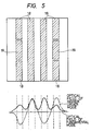
- At least some of the stripe regions, and the corresponding electrodes are divided into parts, with gaps therebetween, to form electrode parts 18 and 19 as shown in Fig. 5.
- a current is applied to all the electrode parts 18 and 19 then oscillation occurs in the highest order mode, and a beam is emitted in a direction ⁇ o .
- current is applied only to the electrode parts 18 in Fig. 5, and not to the electrode parts 19, oscillation occurs in the fundamental mode.
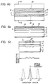
- Fig. 6a is a top view of a fourth embodiment of the present invention, showing a GaAlAs system semiconductor laser
- Fig. 6b is a cross-sectional view taken along line A - A' in Fig. 6a
- Fig. 6c is a cross-sectional view taken along line B - B' in Fig. 6a, the figure also showing a diagram of the refractive index distribution on the B - B' section and the far-field pattern of the emission beam.
- n-GaAs substrate 1 Three grooves which are 3 ⁇ m wide and 1 ⁇ m deep are formed on an n-GaAs substrate 1 by photoetching. The spacing between the centres of the stripes is 5 ⁇ m so that the width of the groove gap is 2 ⁇ m.
- an n-Ga 0.5 Al 0.5 As cladding layer 2 an undoped Ga 0.86 Al 0.14 As active layer 3
- a p-Ga 0.5 Al 0.5 As cladding layer 4 and an n-GaAs layer 5 are sequentially formed by liquid phase growth.
- Zn is then diffused in stripes to form a diffusion region 6 which reaches the p-Ga 0.5 Al 0.5 As cladding layer 4.
- the width of the diffusion region over the groove is less than the groove width by 1 ⁇ m and the width of the diffusion region over the gap between the grooves is less than the width of the groove gap by 0.5 ⁇ m.
- p-electrodes 18,19 are formed only in each stripe region with diffusion by the lift-off method, and after an n-electrode 9 is formed, a laser device having a resonator length of about 300 ⁇ m can be obtained by cleaving.
- the electrode 19, that is, the length of an independent current injection electrode part, is 50 ⁇ m.
- the Zn diffused stripes and the stripe-like electrode thereon causes insulation between the adjacent electrodes.
- the device thus fabricated generates continuous oscillation at room temperature, a threshold current of from 100 to 150 mA and a wavelength of 780 nm, and its oscillation spectrum exhibits a single longitudinal mode.
- Fig. 6c shows its far-field pattern (in a direction parallel to the joint surface).
- the far-field pattern when a current is injected to the p-electrodes 18 and 19 in order to inject the current to all the stripe regions is represented by a dash line in the figure.
- Two emission beams are observed at +4.5° and -4.5° and the full width at half power is 1.5°. This indicates that the highest order mode has been selected.
- the far-field pattern when a current is injected only to the p-electrode 18 is represented by solid line in the drawing.
- One emission beam having a full width at half power of 1.5° is observed at ⁇ 0° and this indicates that the fundamental mode has been selected.
- the fundamental supermode and the highest order supermode can be selected by current injection.
- the selection of both supermodes can be made to an optical output of 300 mW.
- Figs. 7a to 7c show a fifth embodiment of the present invention.
- Fig. 7a is a top view of a laser
- Fig. 7b is a cross-sectional view taken along line A - A' in Fig. 7a
- Fig. 7c is a cross-sectional view taken along line B - B' in Fig. 7a, the figure also including a diagram showing the refractive index distribution.
- n-Ga 0.5 Al 0.5 As cladding layer 2 an undoped Ga 0.86 -Al 0.14 As active layer 3
- a p-Ga 0.55 Al 0.45 As cladding layer 10 and an n-Ga 0.45 Al 0.55 As layer 11 are sequentially formed on an n-GaAs substrate 1 by MOCVD.
- n-Ga 0.45 -Al 0.55 As layer 11 is removed completely by photoetching, four groove stripes which are 3 ⁇ m wide and expose the surface of the p-Ga 0.55 Al 0.45 As cladding layer 10 are formed.
- the spacing between the stripe centres is 6 ⁇ m or in other words, the stripe gap is 3 ⁇ m.
- a buried layer 12 of p-Ga 0.55 Al 0.45 As and a p-GaAs layer 20 are formed by MOCVD.
- p-electrodes 18,19 are formed by a lift-off method and after an n-electrode 9 is formed, a laser device having a resonator which is about 300 ⁇ m long is obtained by cleaving.
- the length of the electrode 19, the independent current injection electrode is 100 ⁇ m.
- the device thus fabricated generates continuous oscillation at room temperature, a threshold current of 100 to 160 mA and a wavelength of 780 nm.
- Current is injected to the p-electrodes 18,19 in order to inject the current to all the stripe regions.
- the resultant far-field pattern exhibits two emission beams (with the full width at half power of 1.5° for each beam) at +4.0° and -4.0°, and thus the highest order supermode is selected.
- the far-field pattern has one emission beam at ⁇ 0° and the fundamental supermode is obtained. In other words, either mode can be selected in a satisfactory manner in the same way as in Embodiment 1 and the radiation angle of the emission beam can be made changeable to an optical output of up to 200 mW.
- Figs. 8a to 8c show a sixth embodiment of the present invention.
- Fig. 8a is a top view of a laser
- Fig. 8b is a cross-sectional view taken along line A - A' in Fig. 8a
- Fig. 8c is a cross-sectional view taken along line B - B' in Fig. 8a, the figure also showing a diagram of the refractive index distribution of the active layer of the laser device.
- a p-Ga 0.5 Al 0.5 As cladding layer 4, a p-Ga 0.55 Al 0.45 As optical guide layer 14, a superlattice active layer 15 formed by alternately laminating five each 100 ⁇ (1 ⁇ 10 ⁇ 10m) thick undoped Ga 0.9 Al 0.1 As well layers and 50 ⁇ thick undoped Ga 0.7 Al 0.3 As barrier layers, an n-Ga 0.5 Al 0.5 As cladding layer 2 and an n-GaAs cap layer 5 are sequentially formed on a p-GaAs substrate 13 by MOCVD.
- Si ions are injected 17 into 3 ⁇ m wide stripe regions 17 and the outer region 17 of the phased-array region so as to reach the p-Ga 0.55 Al 0.45 As optical guide layer 14, thereby forming four stripe regions.
- the spacing between the stripe regions is 7 ⁇ m.
- n-side stripe electrodes 18, 19 are formed by a lift-off method and, after a p-electrode 16 is formed, a laser device having a resonator which is about 300 ⁇ m long is obtained by cleaving.
- the length of the electrode 19, the independent current injection electrode, is 100 ⁇ m.
- the refractive index of the superlattice layer inside the Si ion injection region becomes disordered and mixed.
- the refractive index of this disordered superlattice layer is smaller than that of the superlattice layer which is not disordered.
- the device thus fabricated provides similar effects to those of Embodiments 4 and 5.
- the highest order supermode is selected and when the current is injected only to the n-electrode 18, the fundamental supermode is selected.
- the number of stripes is preferably between 2 and 20.
- the injection of current into the device occurs into parts of the device other than the parts containing the stripe regions, and in particular current is injected by one or more electrodes on one or both sides of the part of the device containing the stripe regions.
- Fig. 9 is a sectional view of a laser device of a seventh embodiment in which the present invention is applied to a GaAlAs system semiconductor laser.
- n-Ga 0.5 Al 0.5 As cladding layer 2 An n-Ga 0.5 Al 0.5 As cladding layer 2, a multi-quantum well active layer 33 formed by alternately laminating six each of 8 nm thick Ga 0.9 Al 0.10 As well layers and 4nm thick Ga 0.70 Al 0.30 As barrier layers, a p-Ga 0.5 Al 0.5 As cladding layer 4 and an n-GaAs current blocking layer 5 are sequentially formed on an n-GaAs substrate crystal 1 by MOCVD. The n-GaAs layer 5 is removed completely by photoetching and three groove stripes are formed which are 4 ⁇ m wide and expose the surface of the p-Ga 0.5 Al 0.5 As cladding layer. At this time, the spacing between the stripe centres is 6 ⁇ m.
- proton (H+) ions are injected to regions outside the phased-array region to form a proton injection region 20.
- the proton ions are injected so that they extend to the n-GaAs current blocking layer 5 or the p-Ga 0.5 Al 0.5 As cladding layer 6.
- the region into which the protons are injected becomes an insulating layer and no current injection occurs into this region.
- a p-electrode 39 and an electrode 40 for applying an electric field are formed on the phased-array region and on the proton injection region 20, respectively, and thus a laser device having a resonator which is about 300 ⁇ m long can be obtained.
- the p-Ga 0.5 Al 0.5 As cladding layer 4 is between 0.1 and 0.5 ⁇ m thick and the laser is thus of a refractive index type. There can thus be obtained a high output phased-array laser having low aberration.
- the device thus fabricated generates continuous oscillation at room temperature, a threshold current of from 100 to 120 mA and a wavelength of 780 nm, and its oscillation spectrum exhibits a single longitudinal mode.
- the voltage of the electrode 40 is zero, two emission beams (each having a full width at half power of 1.5°) are observed at +4.0° and -4.0° in the far-field pattern and thus the highest order supermode has been selected.
- the voltage of the electrode 40 is +5V, one emission beam (full width at half power of 1.5°) is observed at ⁇ 0° in the far-field pattern and the fundamental supermode oscillation is selected.
- the fundamental mode is selected because the effective forbidden band width of the multi-quantum well layer 33 is small due to the application of the field and the loss of the laser beam becomes great.
- a voltage +3 V is applied to the field application electrode 40, two emission beams having the full width at half power of 1.5° are observed at +1.5° and -1.5° and this mode is the secondary supermode.
- all the three kinds of supermodes can be selected freely by changing the voltage to be applied to the electrode 40.
- Fig. 10 shows a cross-sectional view of a laser device.
- n-GaAs cap layer By photoetching the n-GaAs cap layer three n-GaAs 5 ⁇ m wide stripes 16 are produced, and Si ions are injected into the rest of regions so as to reach the active layer 33 and to form a layer 17 which is disordered and mixed Here, the spacing-between the centres of the stripes is 8 ⁇ m.
- An SiO2 film 43 is deposited onto the gaps between the n-GaAs stripes 16, and a p-electrode 44 and an n-electrode 45 are formed. Thereafter, proton ions are injected into the outer parts of the phased-array region to form a proton injection region, and a field application electrode 40 is formed thereon.
- a laser device having a resonator which is about 300 ⁇ m long is then obtained by cleaving.
- the laser device thus fabricated exhibits the similar effects to that of Embodiment 7, and the fundamental supermode and the highest order supermode can be selected independently by applying a voltage to the electrode 40.
- at least one layer of quantum well layers has a thickness less than a De Broglie wavelength of the electron, or that the active layer consists of only one layer having a thickness less than a De Broglie wavelength of the electron.
- each of the Embodiments of the present invention may have any combination of the stripe regions of from 2 to 20 and a stripe gap width of from 1 to 8 ⁇ m.
- a BH structure, a rib-type structure, and similar structures can be used to form the fundamental stripe structure of the present invention as alternatives to the stripe structure described above.
- a semiconductor laser device in accordance with the present invention can be applied in the same way to laser materials other than the GaAlAs system such as an InGaAsP system or an InGaP system.
- the present invention can also be applied to an LOC structure where an optical guide layer is adjacent one side of the active layer, a separate confinement heterostructure (SCH) where the optical layers are adjacent both sides of the active layer and a graded index separate confinement heterostructure (GRIN-SCH) where the refractive index and forbidden band width of the optical guide layers are distributed in the direction of the thickness of the film.
- SCH separate confinement heterostructure
- GRIN-SCH graded index separate confinement heterostructure
- the same effect can be obtained when the conduction types are reversed (such as p to n and n to p).
- the same effect can be obtained by a combination of from 2 to 20 stripes, a stripe region width of from 1 to 10 ⁇ m and the stripe gap width of from 1 to 8 ⁇ m.
- Zn, Si and S may be used as the diffusion impurity for isolation of electrodes of the adjacent stripe electrodes, and Ga, Al, F and B can provide substantially the same effect.
Landscapes
- Physics & Mathematics (AREA)
- Electromagnetism (AREA)
- Optics & Photonics (AREA)
- Condensed Matter Physics & Semiconductors (AREA)
- General Physics & Mathematics (AREA)
- Engineering & Computer Science (AREA)
- Plasma & Fusion (AREA)
- Semiconductor Lasers (AREA)
Claims (14)
- Dispositif laser à semiconducteurs comprenant :
un substrat semiconducteur (1,13);
un résonateur formé sur ledit substrat et comprenant une couche active (3), une pluralité de régions en forme de bandes (30) servant à émettre un faisceau d'émission et une zone d'intervalle entre les régions en forme de bandes;
une première électrode (9,22) située sur ledit substrat à l'opposé du résonateur; et
une pluralité d'électrodes (7,8) situées sur le résonateur;
dans lequel
les régions en forme de bandes (30) sont couplées optiquement et sont agencées de telle sorte que la structure physique du résonateur possède un indice de réfraction à distribution périodique; et
la pluralité des électrodes comprend :
une seconde électrode (7) associée aux régions en forme de bandes pour commander l'injection d'un premier courant dans les régions en forme de bandes; et
une troisième électrode (8) séparée de la seconde électrode (7) pour commander l'injection d'un second courant dans les zones d'intervalle entre les régions en forme de bandes;
l'angle de rayonnement du faisceau d'émission pouvant être modifié par la commande de l'injection des premier et second courants. - Dispositif laser à semiconducteurs comprenant :
un substrat semiconducteur (1,13);
un résonateur formé sur ledit substrat et comprenant une couche active (3,15), une pluralité de régions en forme de bandes servant à émettre un faisceau d'émission et une zone d'intervalle entre les régions en forme de bandes;
une première électrode (9,16) située sur ledit substrat à l'opposé du résonateur; et
une pluralité de secondes électrodes (18,19) situées sur le résonateur;
dans lequel
les régions en forme de bandes sont couplées optiquement et agencées de telle sorte que la structure physique du résonateur possède un indice de réfraction à distribution périodique; et
la pluralité de secondes électrodes associées aux régions en forme de bandes pour la commande de l'injection de courant dans les régions en forme de bandes comprend au moins une électrode (18), qui contient un intervalle définissant des parties séparées (19) de l'électrode, de sorte que les premier et second courants peuvent de ce fait être injectés d'une manière indépendante;
l'angle de rayonnement du faisceau d'émission pouvant être modifié au moyen de la commande de l'injection des premier et second courants. - Dispositif laser à semiconducteurs comprenant :
un substrat semiconducteur (1,41);
un résonateur formé sur ledit substrat et comprenant une couche active (33), une pluralité de régions en forme de bandes pour l'émission d'un faisceau d'émission et une zone d'intervalle entre les régions en forme de bande;
une première électrode (9,45) située sur ledit substrat à l'opposé du résonateur; et
une pluralité d'électrodes (39,40,44) situées sur le résonateur;
dans lequel :
les régions en forme de bandes sont couplées optiquement et disposées de telle sorte que la structure physique du résonateur possède un indice de réfraction à distribution périodique;
la pluralité d'électrodes comprend des seconde et troisième électrodes, la seconde électrode (39,44) étant associée aux régions en forme de bandes servant à commander l'injection du courant dans les régions en forme de bandes, la troisième électrode (40) étant en contact avec au moins une région (20) qui n'est pas située à l'intérieur de la partie du dispositif contenant les régions en forme de bandes, la troisième électrode (40) servant à appliquer des signaux de tension indépendants de signaux envoyés à la seconde électrode, de manière à modifier le mode d'oscillation du résonateur et par conséquent modifier l'angle de rayonnement du faisceau d'émission. - Dispositif selon la revendication 3, dans lequel les signaux électriques appliqués à la troisième électrode (40) sont des signaux de champ électrique.
- Dispositif selon la revendication 4, dans lequel le résonateur comprend des régions (20) d'injection de protons, la troisième électrode (40) est située sur les régions d'injection de protons, et les signaux électriques sont des signaux de tension qui sont appliqués à la troisième électrode sur la zone d'injection de protons.
- Dispositif selon la revendication 5, dans lequel le résonateur comprend en outre une couche (5) de blocage du courant contenant les régions en forme de bandes; la couche active (33) est située entre des couches de revêtement (2,4) qui sont situées entre le substrat (1) et la couche (5) de blocage du courant; et les régions d'injection de protons (20) s'étendent à une profondeur inférieure à celle de la couche active (33).
- Dispositif selon la revendication 6, dans lequel le résonateur comprend en outre une couche formant guide optique (42), située entre la couche de revêtement, qui est située sur le côté du substrat (41), et la couche active (33); les régions en forme de bandes s'étendant à une profondeur inférieure à celle de la couche active (33); et la seconde électrode (44) se situe dans des régions en forme de bandes présélectionnées.
- Dispositif selon l'une quelconque des revendications 5 à 7, dans lequel la couche active (33) est une couche active à puits quantiques multiples.
- Dispositif selon l'une quelconque des revendications 5 à 8, dans lequel des régions isolantes sont disposées au-dessous de la troisième électrode (40).
- Dispositif selon la revendication 9, dans lequel les régions isolantes correspondent aux régions d'injection de protons.
- Dispositif selon l'une quelconque des revendications 1 et 2, dans lequel le résonateur comporte en outre une couche de revêtement (2) située entre ledit substrat (1) et ladite couche active (3), une pluralité de couches semiconductrices comprenant une autre couche de revêtement (4) située sur ladite couche active, et une pluralité de régions diffusées (6) dans ladite pluralité de couches semiconductrices, à une profondeur inférieure a celle de ladite couche active (3), lesdites régions diffusées portant une pluralité d'électrodes (7,8).
- Dispositif selon la revendication 11, dans lequel ladite couche active (3) et lesdites couches de revêtement (2,4) sont situées entre ledit substrat (1) et une couche semiconductrice (11); et lesdites régions en forme de bandes sont situées dans ladite couche semiconductrice (11).
- Dispositif selon la revendication 12, dans lequel le résonateur comprend en outre une pluralité de couches semiconductrices, et une pluralité de régions diffusées (6) sont situées dans ladite pluralité de couches, à une profondeur inférieure à celle de ladite couche active (3), d'une manière qui correspond auxdites régions en forme de bandes et à l'intervalle entre ces régions, et ladite pluralité d'électrodes (7,8) est formée sur lesdites régions diffusées.
- Dispositif selon l'une quelconque des revendications 1 et 2, dans lequel le résonateur comprend en outre une couche formant guide optique et une couche active formant super-réseau (15), lesdites couches étant toutes deux situées entre les couches de revêtement (2,4), et ladite couche formant guide optique (14) étant située entre la couche de revêtement (4) qui est située sur le côté du substrat (13), et ladite couche active de superréseau (15).
Applications Claiming Priority (2)
| Application Number | Priority Date | Filing Date | Title |
|---|---|---|---|
| JP60285519A JP2539368B2 (ja) | 1985-12-20 | 1985-12-20 | 半導体レ−ザ装置 |
| JP285519/85 | 1985-12-20 |
Publications (3)
| Publication Number | Publication Date |
|---|---|
| EP0227426A2 EP0227426A2 (fr) | 1987-07-01 |
| EP0227426A3 EP0227426A3 (en) | 1988-07-27 |
| EP0227426B1 true EP0227426B1 (fr) | 1994-03-23 |
Family
ID=17692581
Family Applications (1)
| Application Number | Title | Priority Date | Filing Date |
|---|---|---|---|
| EP86309843A Expired - Lifetime EP0227426B1 (fr) | 1985-12-20 | 1986-12-17 | Laser à semi-conducteur |
Country Status (5)
| Country | Link |
|---|---|
| US (1) | US4797891A (fr) |
| EP (1) | EP0227426B1 (fr) |
| JP (1) | JP2539368B2 (fr) |
| KR (1) | KR940011107B1 (fr) |
| DE (1) | DE3689742T2 (fr) |
Families Citing this family (10)
| Publication number | Priority date | Publication date | Assignee | Title |
|---|---|---|---|---|
| JP2768672B2 (ja) * | 1987-09-30 | 1998-06-25 | 株式会社日立製作所 | 面発光半導体レーザ |
| JPH0196629A (ja) * | 1987-10-08 | 1989-04-14 | Fuji Photo Film Co Ltd | 光波長変換モジュール |
| JP2728672B2 (ja) * | 1988-02-22 | 1998-03-18 | 株式会社東芝 | 半導体レーザ装置、ダブルヘテロウエハおよびその製造方法 |
| CA2011155C (fr) * | 1989-03-06 | 1994-04-19 | Misuzu Sagawa | Laser a semiconducteurs |
| US4903275A (en) * | 1989-03-20 | 1990-02-20 | General Electric Company | Phase modulation semiconductor laser array |
| US5082595A (en) * | 1990-01-31 | 1992-01-21 | Adhesives Research, Inc. | Method of making an electrically conductive pressure sensitive adhesive |
| DE10239003A1 (de) | 2001-09-17 | 2003-04-03 | Heidelberger Druckmasch Ag | Mehrstrahllaserlichtquelle mit variablem Laserlichtquellenabstand zur Bebilderung von Druckformen |
| US7555896B2 (en) | 2004-03-19 | 2009-07-07 | Ford Global Technologies, Llc | Cylinder deactivation for an internal combustion engine |
| US11322909B2 (en) * | 2016-08-30 | 2022-05-03 | Panasonic Intellectual Property Management Co., Ltd. | Semiconductor laser device |
| US10840406B2 (en) * | 2017-04-17 | 2020-11-17 | Hamamatsu Photonics K.K. | Optical semiconductor element and method of driving optical semiconductor element |
Family Cites Families (7)
| Publication number | Priority date | Publication date | Assignee | Title |
|---|---|---|---|---|
| JPS57164590A (en) * | 1981-04-01 | 1982-10-09 | Fujitsu Ltd | Photosemiconductor device |
| US4378255A (en) * | 1981-05-06 | 1983-03-29 | University Of Illinois Foundation | Method for producing integrated semiconductor light emitter |
| JPS57198680A (en) * | 1981-05-30 | 1982-12-06 | Fujitsu Ltd | Optical semiconductor device |
| US4445218A (en) * | 1981-09-28 | 1984-04-24 | Bell Telephone Laboratories, Incorporated | Semiconductor laser with conductive current mask |
| US4730326A (en) * | 1984-09-12 | 1988-03-08 | Sharp Kabushiki Kaisha | Semiconductor laser array device |
| JPH0666511B2 (ja) * | 1984-11-19 | 1994-08-24 | キヤノン株式会社 | 半導体装置 |
| US4674096A (en) * | 1985-03-04 | 1987-06-16 | California Institute Of Technology | Lateral coupled cavity semiconductor laser |
-
1985
- 1985-12-20 JP JP60285519A patent/JP2539368B2/ja not_active Expired - Lifetime
-
1986
- 1986-12-15 US US06/941,842 patent/US4797891A/en not_active Expired - Fee Related
- 1986-12-16 KR KR1019860010753A patent/KR940011107B1/ko not_active Expired - Fee Related
- 1986-12-17 DE DE3689742T patent/DE3689742T2/de not_active Expired - Fee Related
- 1986-12-17 EP EP86309843A patent/EP0227426B1/fr not_active Expired - Lifetime
Also Published As
| Publication number | Publication date |
|---|---|
| JP2539368B2 (ja) | 1996-10-02 |
| DE3689742T2 (de) | 1994-06-30 |
| JPS62145792A (ja) | 1987-06-29 |
| DE3689742D1 (de) | 1994-04-28 |
| EP0227426A3 (en) | 1988-07-27 |
| US4797891A (en) | 1989-01-10 |
| KR870006688A (ko) | 1987-07-14 |
| KR940011107B1 (ko) | 1994-11-23 |
| EP0227426A2 (fr) | 1987-07-01 |
Similar Documents
| Publication | Publication Date | Title |
|---|---|---|
| US4594718A (en) | Combination index/gain guided semiconductor lasers | |
| US4817110A (en) | Semiconductor laser device | |
| US4318058A (en) | Semiconductor diode laser array | |
| US4328469A (en) | High output power injection lasers | |
| EP0337688B1 (fr) | Batterie de lasers à semi-conducteurs verrouillés en phase utilisant des antiguides espacés étroitement | |
| EP0064339B1 (fr) | Laser sémiconducteur | |
| EP0065818A1 (fr) | Laser à semiconducteur à verrouillage de phase | |
| US4257011A (en) | Semiconductor laser device | |
| US4803691A (en) | Lateral superradiance suppressing diode laser bar | |
| US4823352A (en) | Semiconductor laser with a variable oscillation wavelength | |
| EP0227426B1 (fr) | Laser à semi-conducteur | |
| US4903274A (en) | Semiconductor laser array device | |
| JPH05145175A (ja) | 半導体分布帰還形レーザ装置 | |
| Botez | Laser diodes are power-packed: Single-mode laser diodes have a rosy future, both as individual sources of power up to 100 milliwatts and in arrays promising up to half a watt | |
| US4718069A (en) | Semiconductor laser array with single lobed output | |
| EP0162660B1 (fr) | Dispositif laser semi-conducteur du type à résonateur composé | |
| EP0187718B1 (fr) | Laser à semi-conducteur à réflecteur distribué | |
| US4730326A (en) | Semiconductor laser array device | |
| US4737959A (en) | Semiconductor laser array device | |
| US4866724A (en) | Wide-waveguide interferometric array with interelement losses | |
| JPH055391B2 (fr) | ||
| US4878223A (en) | Semiconductor laser array device | |
| US4771433A (en) | Semiconductor laser device | |
| Stoll | Optimally coupled, GaAs-distributed Bragg reflection lasers | |
| JPH0449274B2 (fr) |
Legal Events
| Date | Code | Title | Description |
|---|---|---|---|
| PUAI | Public reference made under article 153(3) epc to a published international application that has entered the european phase |
Free format text: ORIGINAL CODE: 0009012 |
|
| 17P | Request for examination filed |
Effective date: 19870206 |
|
| AK | Designated contracting states |
Kind code of ref document: A2 Designated state(s): DE FR GB |
|
| PUAL | Search report despatched |
Free format text: ORIGINAL CODE: 0009013 |
|
| AK | Designated contracting states |
Kind code of ref document: A3 Designated state(s): DE FR GB |
|
| 17Q | First examination report despatched |
Effective date: 19910115 |
|
| GRAA | (expected) grant |
Free format text: ORIGINAL CODE: 0009210 |
|
| AK | Designated contracting states |
Kind code of ref document: B1 Designated state(s): DE FR GB |
|
| REF | Corresponds to: |
Ref document number: 3689742 Country of ref document: DE Date of ref document: 19940428 |
|
| ET | Fr: translation filed | ||
| PLBE | No opposition filed within time limit |
Free format text: ORIGINAL CODE: 0009261 |
|
| STAA | Information on the status of an ep patent application or granted ep patent |
Free format text: STATUS: NO OPPOSITION FILED WITHIN TIME LIMIT |
|
| 26N | No opposition filed | ||
| PGFP | Annual fee paid to national office [announced via postgrant information from national office to epo] |
Ref country code: GB Payment date: 19951207 Year of fee payment: 10 |
|
| PGFP | Annual fee paid to national office [announced via postgrant information from national office to epo] |
Ref country code: FR Payment date: 19951220 Year of fee payment: 10 |
|
| PGFP | Annual fee paid to national office [announced via postgrant information from national office to epo] |
Ref country code: DE Payment date: 19960222 Year of fee payment: 10 |
|
| PG25 | Lapsed in a contracting state [announced via postgrant information from national office to epo] |
Ref country code: GB Effective date: 19961217 |
|
| GBPC | Gb: european patent ceased through non-payment of renewal fee |
Effective date: 19961217 |
|
| PG25 | Lapsed in a contracting state [announced via postgrant information from national office to epo] |
Ref country code: FR Effective date: 19970829 |
|
| PG25 | Lapsed in a contracting state [announced via postgrant information from national office to epo] |
Ref country code: DE Effective date: 19970902 |
|
| REG | Reference to a national code |
Ref country code: FR Ref legal event code: ST |