EP0227945A2 - Procédé de fabrication d'une cellule solaire - Google Patents
Procédé de fabrication d'une cellule solaire Download PDFInfo
- Publication number
- EP0227945A2 EP0227945A2 EP86116234A EP86116234A EP0227945A2 EP 0227945 A2 EP0227945 A2 EP 0227945A2 EP 86116234 A EP86116234 A EP 86116234A EP 86116234 A EP86116234 A EP 86116234A EP 0227945 A2 EP0227945 A2 EP 0227945A2
- Authority
- EP
- European Patent Office
- Prior art keywords
- layer
- inversion
- copper
- semiconductor
- electrically conductive
- Prior art date
- Legal status (The legal status is an assumption and is not a legal conclusion. Google has not performed a legal analysis and makes no representation as to the accuracy of the status listed.)
- Withdrawn
Links
Images

Classifications
-
- H—ELECTRICITY
- H10—SEMICONDUCTOR DEVICES; ELECTRIC SOLID-STATE DEVICES NOT OTHERWISE PROVIDED FOR
- H10F—INORGANIC SEMICONDUCTOR DEVICES SENSITIVE TO INFRARED RADIATION, LIGHT, ELECTROMAGNETIC RADIATION OF SHORTER WAVELENGTH OR CORPUSCULAR RADIATION
- H10F10/00—Individual photovoltaic cells, e.g. solar cells
- H10F10/10—Individual photovoltaic cells, e.g. solar cells having potential barriers
- H10F10/16—Photovoltaic cells having only PN heterojunction potential barriers
- H10F10/169—Photovoltaic cells having only PN heterojunction potential barriers comprising Cu2X/CdX heterojunctions, wherein X is a Group VI element, e.g. Cu2O/CdO PN heterojunction photovoltaic cells
-
- H—ELECTRICITY
- H10—SEMICONDUCTOR DEVICES; ELECTRIC SOLID-STATE DEVICES NOT OTHERWISE PROVIDED FOR
- H10F—INORGANIC SEMICONDUCTOR DEVICES SENSITIVE TO INFRARED RADIATION, LIGHT, ELECTROMAGNETIC RADIATION OF SHORTER WAVELENGTH OR CORPUSCULAR RADIATION
- H10F71/00—Manufacture or treatment of devices covered by this subclass
-
- Y—GENERAL TAGGING OF NEW TECHNOLOGICAL DEVELOPMENTS; GENERAL TAGGING OF CROSS-SECTIONAL TECHNOLOGIES SPANNING OVER SEVERAL SECTIONS OF THE IPC; TECHNICAL SUBJECTS COVERED BY FORMER USPC CROSS-REFERENCE ART COLLECTIONS [XRACs] AND DIGESTS
- Y02—TECHNOLOGIES OR APPLICATIONS FOR MITIGATION OR ADAPTATION AGAINST CLIMATE CHANGE
- Y02E—REDUCTION OF GREENHOUSE GAS [GHG] EMISSIONS, RELATED TO ENERGY GENERATION, TRANSMISSION OR DISTRIBUTION
- Y02E10/00—Energy generation through renewable energy sources
- Y02E10/50—Photovoltaic [PV] energy
Definitions
- the invention relates to a photovoltaic cell with a first electrically conductive contact, a first semiconductor layer, a second semiconductor layer of another conductivity type and a second electrically conductive contact, which are arranged in layers one above the other, and one between one of the semiconductor layers and the closest electrically conductive contact arranged by electron and holes tunnelable further layer and a method for producing such.
- the efficiency of a Cu 2 S / CdS thin-film solar cell is strongly dependent on the stoichiometry of the copper sulfide, which takes on the function of the absorber in the solar cell, which has a direct influence on the number of charge carriers formed and on the achievable current density leaves.
- the stoichiometry should be between Cu 1.995 S and Cu 2.000 S. Since this copper sulfide represents the surface of the solar cell system, an interaction with the oxygen in the air or the covering materials used must be considered. This forms copper oxide Cu 2 -z O - (with 0 ⁇ z 51); this obtains its copper atoms from the copper sulfide, which thus acts as a "copper supplier" for the copper oxide.
- the copper sulfide layer is only approx. 300 nm thick and the resulting copper oxide can increase to a thickness of 5-10% of the thickness of the copper sulfide, a sharp decrease in the copper stoichiometry can be observed as a result: the stoichiometry is very good even when present good initial values down to Cu 1.90 S.
- DE-OS 21 52 895 therefore attempts to increase the efficiency of a thin-film solar cell of the copper sulfide / cadmium sulfide type and to maintain it at a high level in that the copper oxide layer formed by degradation is also formed to improve the stoichiometry of the copper sulfide.
- aging of the front-side semiconductor copper sulfide would be included in the manufacturing process of the solar cell.
- a further copper-containing layer is applied to the copper sulfide layer, which is thin compared to the copper sulfide layer.
- the additional layer can e.g. can be obtained by applying an additional layer containing copper and then tempering in vacuum or in air.
- the copper inventory for the additional layer can be generated by reducing the copper sulfide layer on the surface.
- the surface can be reduced by treatment in a glow field in a hydrogen atmosphere.
- the object of the present invention is to develop a photovoltaic cell of the type mentioned at the outset in such a way that it is ensured that a change in the stoichiometry of the semiconductor layers due to depletion as a result of diffusion to the electrically conductive contacts does not occur, without any special requirements being placed on them .
- the layer is a semiconductor inversion layer which is not permeable to ions, that the inversion layer is formed on the semiconductor layer and that a low-resistance layer which conducts the electrons or holes well is arranged between the semiconductor inversion layer and the electrically conductive contact is.
- the formation of the inversion layer on the surface of the second semiconductor layer ensures that a stoichiometry which has been predetermined once is not deteriorated, as a result of which the current density which can be achieved with illumination is not reduced.
- This is achieved by the function of the inversion layer, which namely prevents the tunneling of ions, but allows electrons or holes, i.e. the charge carriers that determine the efficiency of the solar cell (because due to the mass of the ions, which is considerably larger than that of the electrons or holes, compared to the mass of the electrons or holes Tunnel probability becomes negligibly small).
- the inversion layer can have a thickness of approximately 1 to 5 nm.
- the inversion layer arises from the fact that strongly reducing species, such as a negatively charged hydrogen atom H-) interact with the surface of the p-type semiconductor, i.e. the copper sulfide.
- a prerequisite that a corresponding inversion layer is formed is that the copper sulfide layer on the front side represents pure copper sulfide. that neither copper oxide nor excess sulfur ions are present. Since these proportions that disturb the stoichiometry of the copper sulfide layer always occur during the production of the copper sulfide layer, the reduction of copper oxide on the surface of the copper sulfide layer and the removal of free sulfur ions are first carried out according to the invention, followed by adsorption-reducing species and interaction thereof with the p-semiconductor Cu 2.0000 S to convert its surface into the inversion layer.
- the inversion layer would not be formed in the copper sulfide. This is due to the fact that, in the presence of electron holes of the non-highly stoichiometric Cu 2-x S or Cu 2. , 0, the electrons of the adsorbed donors recombine directly with these electron holes, as must be the case in DE-OS 21 52 895 (there the surface layer of copper sulfide is converted to copper without changing the bulk material underneath).
- the inversion layer ensures that there is no degradation of the copper sulfide layer even over long periods of time, that is to say the high stoichiometry once achieved is maintained.
- the pure copper sulfide layer is of high impedance, consequently a charge carrier transport, by which the efficiency of the solar cell is determined, to the electrically conductive front contact is impeded, the reduction is continued in a further embodiment of the invention even after the inversion layer has been built up, by the free surface thereof to convert into pure copper, which is only oxidized to Cu 2-y O in a subsequent annealing process.
- This oxide layer is at least an order of magnitude lower than Cu 2.0000 S and represents a charge carrier connection between the front semiconductor layer and the electrically conductive front contact arranged on the oxide layer.
- the Cu 2-y O layer could also be used if a dense front contact grid would be applied directly to the inversion layer, but this would have the disadvantage that undesirable shading would take place. However, degradation would not occur. Therefore, the copper layer for the copper oxide can also be applied in another process , such as in a vapor deposition process or by galvanic deposition.)
- the discharge known from DE-OS 21 52 895 is modified in a proprietary proposal in such a way that after application of the electrically conductive back contact, the cadmium sulfide and the Cu 2-x S layer, these are preferably used as a unit the positive pillar of the glow discharge can be placed in a hydrogen atmosphere.
- the carrier with the layers arranged thereon is brought into an initially evacuated space (approximately 10- 'mbar (10 -4 Pa)), in order to then use hydrogen at a pressure of approximately 0.5 mbar. (50 Pa) to flood.
- the actual glow discharge takes place, in which hydrogen radicals or H ions reduce the Cu 2-x S layer to such an extent that the highly stoichiometric Cu 2, 0000 S layer is formed, the surface of which is converted into the inversion layer and the surface of which is in turn converted into pure copper. It must be ensured that the reducing species do not merely reduce the surface area of the Cu 2 as described in DE-OS 21 52 895. x S-layer to elemental copper, while the underlying bulk material remains unchanged as Cu 2-x S-layer.
- annealing This can be done either at 180 ° C in air or 200 ° C in vacuum and then at 150 ° C in air.
- the reduction of the Cu 2.0000 S layer after formation of the inversion layer and the annealing result in a controlled oxide formation.
- a defined thickness of the copper oxide is Cu 2 . yO not possible with other manufacturing processes if the copper layer required for the oxide layer is evaporated directly onto the semiconductor on the front.
- oxide from the tempering step and residual oxides that have already been formed during the manufacturing process of the semiconductor layer mix.
- a copper sulfide-cadmium sulfide solar cell (10) is shown purely schematically and in an enlarged representation.
- an adhesive layer (14) in the form of e.g. evaporated or sputtered titanium are applied in order to arrange a first electrically conductive back contact (16) thereon.
- This can consist of silver and can also be applied by vapor deposition or sputtering.
- a layer of cadmium sulfide (18) is then evaporated onto the silver layer (16). This can be treated briefly in aqueous hydrochloric acid to reduce reflections and to etch out grain boundaries.
- the thickness of the cadmium sulfide layer is approximately 10 to 20 ⁇ m.
- a copper sulfide layer (20) (thickness approx. 200-500 nm) is then produced on the cadium sulfide layer (18) by immersing the cadmium sulfide layer (18) in a hot, preferably aqueous copper (I) chloride solution, the Surface of the cadmium sulfide is converted from copper to copper sulfide in an ion exchange process from cadmium to copper.
- This Cu 2-x S layer has a stoichiometry with x, for example from 0.01 to 0.04. At the same time, part of the surface of the copper sulfide layer (20) is oxidized. This Cu 2 . Z with O ⁇ z 1 1 cannot be seen in FIG. 1. This Cu 2 -z O layer and the not highly stoichiometric Cu 2 . x S layer negatively affects the efficiency of the photovoltaic cell (10). In addition, degradation, ie copper depletion, can occur in the copper sulfide layer (20) over a longer period of time.
- the copper sulfide layer (20) is reduced in a controlled manner, namely in a glow discharge in a hydrogen atmosphere.
- the substrate (12) with the layers (14, 16, 18) and (20) is arranged in the region of an anode (32) which is arranged together with a cathode (34) in a glow bowl (30).
- the smoldering vessel (30) is then evacuated to a pressure of approximately 10 -6 mbar (10- 4 Pa). This is followed by controlled flooding with hydrogen to an extent such that a constant pressure of approximately 0.5 mbar (50 Pa) is established. Then the glow discharge takes place.
- the current density is 10 ⁇ A / cm 2 shark lead layer.
- the voltage applied between the electrodes amounts to 300 V.
- the Cu 2.0000 S layer (20) and the inversion layer (24) are high-resistance, care must be taken that a relatively low-resistance layer (26) is applied to them in order to conduct charge carriers through them to a front contact.
- This additional layer (26) is obtained by reducing the free surface of the inversion layer (24) in the glow process, so that a pure copper layer (26) is formed.
- the thickness of this layer is approximately 1 nm and can be specifically adjusted by the glow process.
- the substrate (12) with the layers (14, 16, 18, 20, 24, 26) is then removed from the glow pot (30) in order to be subsequently annealed, for example in a normal atmosphere at 180 ° C. or first in a vacuum at 200 ° C and then in a normal atmosphere at 150 ° C.
- the copper layer (26) is oxidized, that is to say a Cu 2-y CO layer with O ⁇ y ⁇ 1 is formed.
- a front contact (28) is then arranged on this low-resistance layer (26), via which the charge carriers are discharged.
- the solar cell (10) can be encapsulated via cover material and a cover plate (25).
- a correspondingly manufactured solar cell (10) has a highly stoichiometric copper sulfide layer (20) which, due to the inversion layer (24) on its surface, a stoichiometric depletion also over a long period of e.g. 5 to 10 years is not subject. A degradation that negatively influences the lifespan of solar cells (10) therefore does not occur. Inexpensive production results, among other things. in that the thin-film solar cells can be produced over a large area and subjected to the glow process, which is easy to control.
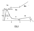
- the process taking place during the glow process in the glow pot (30) can be followed using the H 2 S partial pressure.
- H z S partial pressure (other elements, of course, instead of the H 2 S partial pressure, such as, for example, the H20 formed from the copper oxide, can also be used as parameters).
- the H 2 S partial pressure decreases slightly in order to reach a minimum at time b. If this area can be determined, the duration of which approximately corresponds to that of area I, it can be assumed that the inversion layer (24) has formed. After area II, the H 2 S partial pressure rises continuously in area III. In this area, sulfur is extracted from the surface area of the copper sulfide inversion layer to form H2S. At the same time, copper is formed.
- the thickness of the copper layer and thus ultimately the thickness of the copper oxide layer can be adjusted in a controlled manner in the period c -b.
- the area of area I to area II must be in the ratio of (2.5 + 0.5) to 1. Are these values observed and is also the maxi mum of area I shifted towards a shorter time, it is ensured that the finished thin-film solar cell (10) has the structure according to the invention.
- the teaching according to the invention applies not only to the “front wall” solar cell (10) described, in which the copper sulfide is the upper semiconductor layer (20) facing the front contact (28). Rather, this teaching also applies to the manufacture of a "backwall” solar cell, if the structure of the solar cell is glass (12) / transparent front contact (e.g. SnO x ) (14, 16) / CdS layer (18) / Cu 2nd x S layer (20) / back contact - (28) the copper sulfide is the lower semiconductor layer facing the rear electrically conductive contact.
Landscapes
- Photovoltaic Devices (AREA)
Applications Claiming Priority (2)
| Application Number | Priority Date | Filing Date | Title |
|---|---|---|---|
| DE19853542116 DE3542116A1 (de) | 1985-11-28 | 1985-11-28 | Photovoltaische zelle |
| DE3542116 | 1985-11-28 |
Publications (2)
| Publication Number | Publication Date |
|---|---|
| EP0227945A2 true EP0227945A2 (fr) | 1987-07-08 |
| EP0227945A3 EP0227945A3 (fr) | 1989-03-22 |
Family
ID=6287103
Family Applications (1)
| Application Number | Title | Priority Date | Filing Date |
|---|---|---|---|
| EP86116234A Withdrawn EP0227945A3 (fr) | 1985-11-28 | 1986-11-24 | Procédé de fabrication d'une cellule solaire |
Country Status (3)
| Country | Link |
|---|---|
| US (1) | US4709119A (fr) |
| EP (1) | EP0227945A3 (fr) |
| DE (1) | DE3542116A1 (fr) |
Families Citing this family (6)
| Publication number | Priority date | Publication date | Assignee | Title |
|---|---|---|---|---|
| US4953577A (en) * | 1989-07-06 | 1990-09-04 | Solarex Corporation | Spray encapsulation of photovoltaic modules |
| US5541118A (en) * | 1995-05-22 | 1996-07-30 | Midwest Research Institute | Process for producing cadmium sulfide on a cadmium telluride surface |
| US20090211623A1 (en) * | 2008-02-25 | 2009-08-27 | Suniva, Inc. | Solar module with solar cell having crystalline silicon p-n homojunction and amorphous silicon heterojunctions for surface passivation |
| US8076175B2 (en) * | 2008-02-25 | 2011-12-13 | Suniva, Inc. | Method for making solar cell having crystalline silicon P-N homojunction and amorphous silicon heterojunctions for surface passivation |
| CN102931243A (zh) * | 2011-08-10 | 2013-02-13 | 无锡尚德太阳能电力有限公司 | 碲化镉薄膜太阳电池及其制备方法 |
| US20140283906A1 (en) * | 2013-03-21 | 2014-09-25 | California Institute Of Technology | System and method for controlling an inversion layer in a photovoltaic device |
Family Cites Families (8)
| Publication number | Priority date | Publication date | Assignee | Title |
|---|---|---|---|---|
| US3888697A (en) * | 1971-10-23 | 1975-06-10 | Licentia Gmbh | Photocell |
| DE2846096C2 (de) * | 1978-10-23 | 1985-01-10 | Rudolf Dipl.-Phys. Dr. 8521 Spardorf Hezel | Solarzelle aus Halbleitermaterial |
| US4200473A (en) * | 1979-03-12 | 1980-04-29 | Rca Corporation | Amorphous silicon Schottky barrier solar cells incorporating a thin insulating layer and a thin doped layer |
| US4251286A (en) * | 1979-09-18 | 1981-02-17 | The University Of Delaware | Thin film photovoltaic cells having blocking layers |
| DE3135933A1 (de) * | 1980-09-26 | 1982-05-19 | Unisearch Ltd., Kensington, New South Wales | Solarzelle und verfahren zu ihrer herstellung |
| US4366336A (en) * | 1980-10-16 | 1982-12-28 | Chevron Research Company | Age and heat stabilized photovoltaic cells |
| EP0091998A1 (fr) * | 1982-03-08 | 1983-10-26 | Prutec Limited | Cellules solaires en sulfure de cadmium |
| FR2536913B1 (fr) * | 1982-11-25 | 1986-04-04 | Saint Gobain Rech Sa | Perfectionnement aux cellules photovoltaiques a couche polycristalline a base de cds |
-
1985
- 1985-11-28 DE DE19853542116 patent/DE3542116A1/de active Granted
-
1986
- 1986-11-24 EP EP86116234A patent/EP0227945A3/fr not_active Withdrawn
- 1986-11-28 US US06/936,090 patent/US4709119A/en not_active Expired - Fee Related
Also Published As
| Publication number | Publication date |
|---|---|
| EP0227945A3 (fr) | 1989-03-22 |
| US4709119A (en) | 1987-11-24 |
| DE3542116A1 (de) | 1987-06-04 |
| DE3542116C2 (fr) | 1990-06-21 |
Similar Documents
| Publication | Publication Date | Title |
|---|---|---|
| DE19912961B4 (de) | Halbleiterdünnfilm, Herstellungsverfahren dafür, sowie den Halbleiterdünnfilm aufweisende Solarzelle | |
| EP0468094B1 (fr) | Procédé de fabrication d'une cellule solaire en chalcopyrite | |
| DE4442824C1 (de) | Solarzelle mit Chalkopyrit-Absorberschicht | |
| DE10151415A1 (de) | Solarzelle | |
| DE2755500A1 (de) | Solarzelle und verfahren zu ihrer herstellung | |
| DE102011050089B4 (de) | Verfahren zum Herstellen von elektrischen Kontakten an einer Solarzelle, Solarzelle und Verfahren zum Herstellen eines Rückseiten-Kontaktes einer Solarzelle | |
| DE102005029484A1 (de) | Verbundsolarzelle und Prozess zur Herstellung derselben | |
| DE102011054795A1 (de) | Verfahren zum Abscheiden von Cadmiumsulfid-Schichten mittels zerstäuben zum Einsatz in photovoltaischen Dünnfilmvorrichtungen auf Cadmiumtellurid-Grundlage | |
| DE102012215041A1 (de) | Verfahren zur Herstellung eines Halbleiterelementes eines direktkonvertierenden Röntgendetektors | |
| EP0224231B1 (fr) | Procédé de fabrication d'une cellule solaire en film mince | |
| WO2011047875A2 (fr) | Procédé de dépôt pulsé galvanique induit par la lumière pour la production d'une couche de germination destinée à un contact métallique d'une cellule solaire et pour le renforcement consécutif de cette couche de germination ou de ce contact métallique et dispositif pour la mise en oeuvre du procédé | |
| DE3542116C2 (fr) | ||
| DE19735803B4 (de) | Elektrode-Elektrolyt-Anordnung, Verfahren zur Herstellung einer Elektrode-Elektrolyt-Anordnung und Verwendung einer Elektrode-Elektrolyt-Anordnung | |
| DE10259258B4 (de) | Verfahren zur Herstellung einer Verbindungshalbleiterschicht mit Alkalimetallzusatz | |
| EP2028695A1 (fr) | Procédé destiné à la production d'une couche d'oxyde conductrice transparente | |
| DE112016006557B4 (de) | Verfahren zur Herstellung einer CdTe-Dünnschichtsolarzelle | |
| DE2007261B2 (de) | Elektrische Widerstandssubstanz, insbesondere Widerstandsschicht und Verfahren zu deren Herstellung | |
| DE102014223485A1 (de) | Schichtaufbau für eine Dünnschichtsolarzelle und Herstellungsverfahren | |
| DE19611996C1 (de) | Solarzelle mit einer Chalkopyritabsorberschicht und Verfahren zu ihrer Herstellung | |
| DE10004733C2 (de) | Dünnfilm-Halbleiterbauelement mit einer Chalkopyritschicht und Verfahren zu seiner Herstellung sowie Verwendung des Verfahrens zur Herstellung einer Dünnfilm-Solarzelle | |
| DE102006039331B4 (de) | Photovoltaik-Dünnschichtaufbau und Herstellungsverfahren | |
| DE3434552A1 (de) | Verfahren zur bildung einer pn-grenzschicht | |
| DE102006004909A1 (de) | Verfahren zum Aufbringen von Alkaliionen auf die Oberfläche der CIGSSe-Absorberschicht einer Chalkopyrit-Solarzelle | |
| DE2152895C3 (de) | Dünnschichtphotozelle und Verfahren zu ihrer Herstellung | |
| DE2624394C3 (de) | Photoleitende Ladungsspeicherplatte |
Legal Events
| Date | Code | Title | Description |
|---|---|---|---|
| PUAI | Public reference made under article 153(3) epc to a published international application that has entered the european phase |
Free format text: ORIGINAL CODE: 0009012 |
|
| AK | Designated contracting states |
Kind code of ref document: A2 Designated state(s): DE ES FR IT |
|
| PUAL | Search report despatched |
Free format text: ORIGINAL CODE: 0009013 |
|
| AK | Designated contracting states |
Kind code of ref document: A3 Designated state(s): DE ES FR IT |
|
| 17P | Request for examination filed |
Effective date: 19890308 |
|
| 17Q | First examination report despatched |
Effective date: 19901123 |
|
| RAP1 | Party data changed (applicant data changed or rights of an application transferred) |
Owner name: NUKEM GMBH |
|
| APAB | Appeal dossier modified |
Free format text: ORIGINAL CODE: EPIDOS NOAPE |
|
| STAA | Information on the status of an ep patent application or granted ep patent |
Free format text: STATUS: THE APPLICATION HAS BEEN WITHDRAWN |
|
| 18W | Application withdrawn |
Withdrawal date: 19960606 |
|
| APAF | Appeal reference modified |
Free format text: ORIGINAL CODE: EPIDOSCREFNE |
|
| RIN1 | Information on inventor provided before grant (corrected) |
Inventor name: WOERNER, JOERG, DR. |