EP0228295A2 - Method for producing an electronic device having a multi-layer structure - Google Patents
Method for producing an electronic device having a multi-layer structure Download PDFInfo
- Publication number
- EP0228295A2 EP0228295A2 EP86310163A EP86310163A EP0228295A2 EP 0228295 A2 EP0228295 A2 EP 0228295A2 EP 86310163 A EP86310163 A EP 86310163A EP 86310163 A EP86310163 A EP 86310163A EP 0228295 A2 EP0228295 A2 EP 0228295A2
- Authority
- EP
- European Patent Office
- Prior art keywords
- electronic device
- producing
- gaseous
- starting material
- film
- Prior art date
- Legal status (The legal status is an assumption and is not a legal conclusion. Google has not performed a legal analysis and makes no representation as to the accuracy of the status listed.)
- Granted
Links
Images


Classifications
-
- H—ELECTRICITY
- H10—SEMICONDUCTOR DEVICES; ELECTRIC SOLID-STATE DEVICES NOT OTHERWISE PROVIDED FOR
- H10P—GENERIC PROCESSES OR APPARATUS FOR THE MANUFACTURE OR TREATMENT OF DEVICES COVERED BY CLASS H10
- H10P14/00—Formation of materials, e.g. in the shape of layers or pillars
- H10P14/20—Formation of materials, e.g. in the shape of layers or pillars of semiconductor materials
- H10P14/29—Formation of materials, e.g. in the shape of layers or pillars of semiconductor materials characterised by the substrates
- H10P14/2901—Materials
- H10P14/2923—Materials being conductive materials, e.g. metallic silicides
-
- C—CHEMISTRY; METALLURGY
- C23—COATING METALLIC MATERIAL; COATING MATERIAL WITH METALLIC MATERIAL; CHEMICAL SURFACE TREATMENT; DIFFUSION TREATMENT OF METALLIC MATERIAL; COATING BY VACUUM EVAPORATION, BY SPUTTERING, BY ION IMPLANTATION OR BY CHEMICAL VAPOUR DEPOSITION, IN GENERAL; INHIBITING CORROSION OF METALLIC MATERIAL OR INCRUSTATION IN GENERAL
- C23C—COATING METALLIC MATERIAL; COATING MATERIAL WITH METALLIC MATERIAL; SURFACE TREATMENT OF METALLIC MATERIAL BY DIFFUSION INTO THE SURFACE, BY CHEMICAL CONVERSION OR SUBSTITUTION; COATING BY VACUUM EVAPORATION, BY SPUTTERING, BY ION IMPLANTATION OR BY CHEMICAL VAPOUR DEPOSITION, IN GENERAL
- C23C16/00—Chemical coating by decomposition of gaseous compounds, without leaving reaction products of surface material in the coating, i.e. chemical vapour deposition [CVD] processes
- C23C16/02—Pretreatment of the material to be coated
-
- C—CHEMISTRY; METALLURGY
- C23—COATING METALLIC MATERIAL; COATING MATERIAL WITH METALLIC MATERIAL; CHEMICAL SURFACE TREATMENT; DIFFUSION TREATMENT OF METALLIC MATERIAL; COATING BY VACUUM EVAPORATION, BY SPUTTERING, BY ION IMPLANTATION OR BY CHEMICAL VAPOUR DEPOSITION, IN GENERAL; INHIBITING CORROSION OF METALLIC MATERIAL OR INCRUSTATION IN GENERAL
- C23C—COATING METALLIC MATERIAL; COATING MATERIAL WITH METALLIC MATERIAL; SURFACE TREATMENT OF METALLIC MATERIAL BY DIFFUSION INTO THE SURFACE, BY CHEMICAL CONVERSION OR SUBSTITUTION; COATING BY VACUUM EVAPORATION, BY SPUTTERING, BY ION IMPLANTATION OR BY CHEMICAL VAPOUR DEPOSITION, IN GENERAL
- C23C16/00—Chemical coating by decomposition of gaseous compounds, without leaving reaction products of surface material in the coating, i.e. chemical vapour deposition [CVD] processes
- C23C16/44—Chemical coating by decomposition of gaseous compounds, without leaving reaction products of surface material in the coating, i.e. chemical vapour deposition [CVD] processes characterised by the method of coating
- C23C16/48—Chemical coating by decomposition of gaseous compounds, without leaving reaction products of surface material in the coating, i.e. chemical vapour deposition [CVD] processes characterised by the method of coating by irradiation, e.g. photolysis, radiolysis, particle radiation
- C23C16/482—Chemical coating by decomposition of gaseous compounds, without leaving reaction products of surface material in the coating, i.e. chemical vapour deposition [CVD] processes characterised by the method of coating by irradiation, e.g. photolysis, radiolysis, particle radiation using incoherent light, UV to IR, e.g. lamps
-
- C—CHEMISTRY; METALLURGY
- C23—COATING METALLIC MATERIAL; COATING MATERIAL WITH METALLIC MATERIAL; CHEMICAL SURFACE TREATMENT; DIFFUSION TREATMENT OF METALLIC MATERIAL; COATING BY VACUUM EVAPORATION, BY SPUTTERING, BY ION IMPLANTATION OR BY CHEMICAL VAPOUR DEPOSITION, IN GENERAL; INHIBITING CORROSION OF METALLIC MATERIAL OR INCRUSTATION IN GENERAL
- C23C—COATING METALLIC MATERIAL; COATING MATERIAL WITH METALLIC MATERIAL; SURFACE TREATMENT OF METALLIC MATERIAL BY DIFFUSION INTO THE SURFACE, BY CHEMICAL CONVERSION OR SUBSTITUTION; COATING BY VACUUM EVAPORATION, BY SPUTTERING, BY ION IMPLANTATION OR BY CHEMICAL VAPOUR DEPOSITION, IN GENERAL
- C23C16/00—Chemical coating by decomposition of gaseous compounds, without leaving reaction products of surface material in the coating, i.e. chemical vapour deposition [CVD] processes
- C23C16/44—Chemical coating by decomposition of gaseous compounds, without leaving reaction products of surface material in the coating, i.e. chemical vapour deposition [CVD] processes characterised by the method of coating
- C23C16/48—Chemical coating by decomposition of gaseous compounds, without leaving reaction products of surface material in the coating, i.e. chemical vapour deposition [CVD] processes characterised by the method of coating by irradiation, e.g. photolysis, radiolysis, particle radiation
- C23C16/483—Chemical coating by decomposition of gaseous compounds, without leaving reaction products of surface material in the coating, i.e. chemical vapour deposition [CVD] processes characterised by the method of coating by irradiation, e.g. photolysis, radiolysis, particle radiation using coherent light, UV to IR, e.g. lasers
-
- G—PHYSICS
- G03—PHOTOGRAPHY; CINEMATOGRAPHY; ANALOGOUS TECHNIQUES USING WAVES OTHER THAN OPTICAL WAVES; ELECTROGRAPHY; HOLOGRAPHY
- G03G—ELECTROGRAPHY; ELECTROPHOTOGRAPHY; MAGNETOGRAPHY
- G03G5/00—Recording-members for original recording by exposure, e.g. to light, to heat or to electrons; Manufacture thereof; Selection of materials therefor
- G03G5/02—Charge-receiving layers
- G03G5/04—Photoconductive layers; Charge-generation layers or charge-transporting layers; Additives therefor; Binders therefor
- G03G5/08—Photoconductive layers; Charge-generation layers or charge-transporting layers; Additives therefor; Binders therefor characterised by the photoconductive material being inorganic
- G03G5/082—Photoconductive layers; Charge-generation layers or charge-transporting layers; Additives therefor; Binders therefor characterised by the photoconductive material being inorganic and not being incorporated in a bonding material, e.g. vacuum deposited
- G03G5/08214—Silicon-based
- G03G5/08235—Silicon-based comprising three or four silicon-based layers
-
- H—ELECTRICITY
- H10—SEMICONDUCTOR DEVICES; ELECTRIC SOLID-STATE DEVICES NOT OTHERWISE PROVIDED FOR
- H10F—INORGANIC SEMICONDUCTOR DEVICES SENSITIVE TO INFRARED RADIATION, LIGHT, ELECTROMAGNETIC RADIATION OF SHORTER WAVELENGTH OR CORPUSCULAR RADIATION
- H10F10/00—Individual photovoltaic cells, e.g. solar cells
- H10F10/10—Individual photovoltaic cells, e.g. solar cells having potential barriers
- H10F10/17—Photovoltaic cells having only PIN junction potential barriers
-
- H—ELECTRICITY
- H10—SEMICONDUCTOR DEVICES; ELECTRIC SOLID-STATE DEVICES NOT OTHERWISE PROVIDED FOR
- H10F—INORGANIC SEMICONDUCTOR DEVICES SENSITIVE TO INFRARED RADIATION, LIGHT, ELECTROMAGNETIC RADIATION OF SHORTER WAVELENGTH OR CORPUSCULAR RADIATION
- H10F30/00—Individual radiation-sensitive semiconductor devices in which radiation controls the flow of current through the devices, e.g. photodetectors
- H10F30/10—Individual radiation-sensitive semiconductor devices in which radiation controls the flow of current through the devices, e.g. photodetectors the devices being sensitive to infrared radiation, visible or ultraviolet radiation, and having no potential barriers, e.g. photoresistors
- H10F30/15—Individual radiation-sensitive semiconductor devices in which radiation controls the flow of current through the devices, e.g. photodetectors the devices being sensitive to infrared radiation, visible or ultraviolet radiation, and having no potential barriers, e.g. photoresistors comprising amorphous semiconductors
-
- H—ELECTRICITY
- H10—SEMICONDUCTOR DEVICES; ELECTRIC SOLID-STATE DEVICES NOT OTHERWISE PROVIDED FOR
- H10F—INORGANIC SEMICONDUCTOR DEVICES SENSITIVE TO INFRARED RADIATION, LIGHT, ELECTROMAGNETIC RADIATION OF SHORTER WAVELENGTH OR CORPUSCULAR RADIATION
- H10F71/00—Manufacture or treatment of devices covered by this subclass
- H10F71/10—Manufacture or treatment of devices covered by this subclass the devices comprising amorphous semiconductor material
- H10F71/103—Manufacture or treatment of devices covered by this subclass the devices comprising amorphous semiconductor material including only Group IV materials
-
- H—ELECTRICITY
- H10—SEMICONDUCTOR DEVICES; ELECTRIC SOLID-STATE DEVICES NOT OTHERWISE PROVIDED FOR
- H10P—GENERIC PROCESSES OR APPARATUS FOR THE MANUFACTURE OR TREATMENT OF DEVICES COVERED BY CLASS H10
- H10P14/00—Formation of materials, e.g. in the shape of layers or pillars
- H10P14/20—Formation of materials, e.g. in the shape of layers or pillars of semiconductor materials
- H10P14/24—Formation of materials, e.g. in the shape of layers or pillars of semiconductor materials using chemical vapour deposition [CVD]
-
- H—ELECTRICITY
- H10—SEMICONDUCTOR DEVICES; ELECTRIC SOLID-STATE DEVICES NOT OTHERWISE PROVIDED FOR
- H10P—GENERIC PROCESSES OR APPARATUS FOR THE MANUFACTURE OR TREATMENT OF DEVICES COVERED BY CLASS H10
- H10P14/00—Formation of materials, e.g. in the shape of layers or pillars
- H10P14/20—Formation of materials, e.g. in the shape of layers or pillars of semiconductor materials
- H10P14/29—Formation of materials, e.g. in the shape of layers or pillars of semiconductor materials characterised by the substrates
- H10P14/2901—Materials
- H10P14/2922—Materials being non-crystalline insulating materials, e.g. glass or polymers
-
- H—ELECTRICITY
- H10—SEMICONDUCTOR DEVICES; ELECTRIC SOLID-STATE DEVICES NOT OTHERWISE PROVIDED FOR
- H10P—GENERIC PROCESSES OR APPARATUS FOR THE MANUFACTURE OR TREATMENT OF DEVICES COVERED BY CLASS H10
- H10P14/00—Formation of materials, e.g. in the shape of layers or pillars
- H10P14/20—Formation of materials, e.g. in the shape of layers or pillars of semiconductor materials
- H10P14/32—Formation of materials, e.g. in the shape of layers or pillars of semiconductor materials characterised by intermediate layers between substrates and deposited layers
- H10P14/3202—Materials thereof
- H10P14/3204—Materials thereof being Group IVA semiconducting materials
- H10P14/3211—Silicon, silicon germanium or germanium
-
- H—ELECTRICITY
- H10—SEMICONDUCTOR DEVICES; ELECTRIC SOLID-STATE DEVICES NOT OTHERWISE PROVIDED FOR
- H10P—GENERIC PROCESSES OR APPARATUS FOR THE MANUFACTURE OR TREATMENT OF DEVICES COVERED BY CLASS H10
- H10P14/00—Formation of materials, e.g. in the shape of layers or pillars
- H10P14/20—Formation of materials, e.g. in the shape of layers or pillars of semiconductor materials
- H10P14/32—Formation of materials, e.g. in the shape of layers or pillars of semiconductor materials characterised by intermediate layers between substrates and deposited layers
- H10P14/3242—Structure
- H10P14/3244—Layer structure
- H10P14/3251—Layer structure consisting of three or more layers
-
- H—ELECTRICITY
- H10—SEMICONDUCTOR DEVICES; ELECTRIC SOLID-STATE DEVICES NOT OTHERWISE PROVIDED FOR
- H10P—GENERIC PROCESSES OR APPARATUS FOR THE MANUFACTURE OR TREATMENT OF DEVICES COVERED BY CLASS H10
- H10P14/00—Formation of materials, e.g. in the shape of layers or pillars
- H10P14/20—Formation of materials, e.g. in the shape of layers or pillars of semiconductor materials
- H10P14/34—Deposited materials, e.g. layers
- H10P14/3402—Deposited materials, e.g. layers characterised by the chemical composition
- H10P14/3404—Deposited materials, e.g. layers characterised by the chemical composition being Group IVA materials
- H10P14/3411—Silicon, silicon germanium or germanium
-
- H—ELECTRICITY
- H10—SEMICONDUCTOR DEVICES; ELECTRIC SOLID-STATE DEVICES NOT OTHERWISE PROVIDED FOR
- H10P—GENERIC PROCESSES OR APPARATUS FOR THE MANUFACTURE OR TREATMENT OF DEVICES COVERED BY CLASS H10
- H10P14/00—Formation of materials, e.g. in the shape of layers or pillars
- H10P14/20—Formation of materials, e.g. in the shape of layers or pillars of semiconductor materials
- H10P14/34—Deposited materials, e.g. layers
- H10P14/3438—Doping during depositing
- H10P14/3441—Conductivity type
- H10P14/3442—N-type
-
- H—ELECTRICITY
- H10—SEMICONDUCTOR DEVICES; ELECTRIC SOLID-STATE DEVICES NOT OTHERWISE PROVIDED FOR
- H10P—GENERIC PROCESSES OR APPARATUS FOR THE MANUFACTURE OR TREATMENT OF DEVICES COVERED BY CLASS H10
- H10P14/00—Formation of materials, e.g. in the shape of layers or pillars
- H10P14/20—Formation of materials, e.g. in the shape of layers or pillars of semiconductor materials
- H10P14/34—Deposited materials, e.g. layers
- H10P14/3438—Doping during depositing
- H10P14/3441—Conductivity type
- H10P14/3444—P-type
-
- Y—GENERAL TAGGING OF NEW TECHNOLOGICAL DEVELOPMENTS; GENERAL TAGGING OF CROSS-SECTIONAL TECHNOLOGIES SPANNING OVER SEVERAL SECTIONS OF THE IPC; TECHNICAL SUBJECTS COVERED BY FORMER USPC CROSS-REFERENCE ART COLLECTIONS [XRACs] AND DIGESTS
- Y02—TECHNOLOGIES OR APPLICATIONS FOR MITIGATION OR ADAPTATION AGAINST CLIMATE CHANGE
- Y02E—REDUCTION OF GREENHOUSE GAS [GHG] EMISSIONS, RELATED TO ENERGY GENERATION, TRANSMISSION OR DISTRIBUTION
- Y02E10/00—Energy generation through renewable energy sources
- Y02E10/50—Photovoltaic [PV] energy
- Y02E10/548—Amorphous silicon PV cells
-
- Y—GENERAL TAGGING OF NEW TECHNOLOGICAL DEVELOPMENTS; GENERAL TAGGING OF CROSS-SECTIONAL TECHNOLOGIES SPANNING OVER SEVERAL SECTIONS OF THE IPC; TECHNICAL SUBJECTS COVERED BY FORMER USPC CROSS-REFERENCE ART COLLECTIONS [XRACs] AND DIGESTS
- Y02—TECHNOLOGIES OR APPLICATIONS FOR MITIGATION OR ADAPTATION AGAINST CLIMATE CHANGE
- Y02P—CLIMATE CHANGE MITIGATION TECHNOLOGIES IN THE PRODUCTION OR PROCESSING OF GOODS
- Y02P70/00—Climate change mitigation technologies in the production process for final industrial or consumer products
- Y02P70/50—Manufacturing or production processes characterised by the final manufactured product
-
- Y—GENERAL TAGGING OF NEW TECHNOLOGICAL DEVELOPMENTS; GENERAL TAGGING OF CROSS-SECTIONAL TECHNOLOGIES SPANNING OVER SEVERAL SECTIONS OF THE IPC; TECHNICAL SUBJECTS COVERED BY FORMER USPC CROSS-REFERENCE ART COLLECTIONS [XRACs] AND DIGESTS
- Y10—TECHNICAL SUBJECTS COVERED BY FORMER USPC
- Y10S—TECHNICAL SUBJECTS COVERED BY FORMER USPC CROSS-REFERENCE ART COLLECTIONS [XRACs] AND DIGESTS
- Y10S438/00—Semiconductor device manufacturing: process
- Y10S438/909—Controlled atmosphere
Definitions
- This invention relates to an electronic device having a multi-layer structure such as thin film semiconductor device, photovoltaic device, image forming member for electrophotography, etc., and a method for producing the same.
- functional films i.e., semiconductor thin films for electronic devices such as thin film semiconductor devices, imaging devices, etc., particularly amorphous or polycrystalline semiconductor films, are formed individually by suitable film forming methods from the standpoint of desired physical characteristics, uses, etc.
- a silicon deposited film such as amorphous or polycrystalline, i.e., non- single crystalline, silicon film which is optionally compensated for lone pair electrons with a compensating agent such as hydrogen atoms (H) or halogen atoms (X), etc., (hereinafter abbreviated as "NON-Si (H,X)", particularly “A-Si (H,X)” when indicating amorphous silicon and "poly-Si (H,X)” when indicating polycrystalline silicon; the so-called microcrystalline silicon is included within the category of A-Si (H,X) as a matter of course), there have been employed as an attempt the vacuum vapor deposition method, the plasma CVD (PCVD) method, the thermal CVD method, the reactive sputtering method, the ion plating method, the optical CVD method, etc. Generally, the plasma CVD method has been widely and industrialized.
- a compensating agent such as hydrogen atoms (H) or halogen
- Fig. 4 an image forming member for electrophotography as an example.
- a layer constitution, on a substrate 400 made of aluminum consisting of a charge injection preventing layer (first layer, amorphous silicon layer doped with boron B) 401, a photosensitive layer (second layer, amorphous layer not doped with impurities such as B) 402 and a surface protective layer (third layer, amorphous silicon carbide layer) 403 respectively deposited.
- An object of the present invention is to remove such drawbacks of a method for forming a deposited film as described above and at the same time to provide a novel method for producing an electronic device without the use of the formation method of the prior art and an electronic device obtained thereby.
- Another object of the present invention is to provide a method for forming a deposited film capable of obtaining a deposited film with improved interface characteristics over a large area with easy control of film quality and conservation of energy.
- Still another object of the present invention is to provide a method for producing an electronic device having a multi-layer structure which is excellent in productivity and bulk productivity, having high quality as well as excellent physical characteristics such as electrical, optical and semiconductor characteristics.
- a method for producing an electronic device having a multi-layer structure comprising one or more semiconductor thin layers controlled in band gap formed on a substrate, which comprises forming at least one of said semiconductor thin layers controlled in band gap according to the optical CVD method and forming at least one of other constituent layers according to the method comprising introducing a gaseous starting material for formation of a deposited film and a gaseous halogenic oxidizing agent having the property of oxidation action for said starting material into a reaction space to effect chemical contact therebetween to thereby form a plural number of precursors containing a precursor under excited state and transferring at least one precursor of those precursors into a film forming space communicated with the reaction space as a feeding source for the constituent element of the deposited film (hereinafter abbreviated as FOCVD) and an electronic device obtained thereby.
- FOCVD constituent element of the deposited film
- a deposited film having a multi-layer constitution improved in interface characteristics is obtained and simplification of control and bulk production can be effected with full satisfaction of enlargement of area, uniformity of film thickness and uniformity of film quality simultaneously with conservation of energy, without requiring no enormous installation investment for bulk production apparatus, and also control items for bulk production is clarified to afford broad tolerance limit and simple control of apparatus.
- the gaseous starting material to be used for formation of a deposited film is to receive oxidizing action through chemical contact with the gaseous halogenic oxidizing agent and can be selected suitably as desired depending on the kind, characteristic, use, etc., of a deposited film to be obtained.
- the above gaseous starting material and the gaseous halogenic oxidizing agent have only to be made gaseous during chemical contact when introduced into a reaction space, and they can be either liquid or solid as ordinary state.
- the starting material for formation of a deposited film or the halogenic oxidizing agent is liquid or solid, it is introduced in gaseous state into the reaction space through performing bubbling with the use of a carrier gas such as Ar, He, N 2 0 H 2 , etc. optionally with application of heat.
- a carrier gas such as Ar, He, N 2 0 H 2 , etc. optionally with application of heat.
- the partial pressures and mixing ratio of the above gaseous starting material and the gaseous halogenic oxidizing agent may be set by controlling the flow rate of the carrier gas and the vapor pressures of the starting material for formation of a deposited film and the gaseous halogenic oxidizing agent.
- straight or branched chain silane compounds, cyclic silane compounds, chain germanium compounds, etc. may be employed as an effective one.
- examples of branched chain silane compounds include SiH 3 SiH(SiH 3 ) SiH 2 SiH 3
- these starting materials may be used either as a single kind or as a mixture of two or more kinds, and may also be used as the starting material gas in the case of forming a deposited film according to the optical CVD method.
- the halogenic oxidizing agent to be used in the present invention is to be made gaseous when introduced into the reaction space and at the same time has the property of effectively oxidizing the gaseous starting material for formation of a deposited film introduced into the reaction space by mere chemical contact therewith, including halogen gases such as F 2 , Cl 2 , Br 2 , I 2 , etc., and fluorine, chlorine, bromine, etc., under nascent state as an effective one.
- halogen gases such as F 2 , Cl 2 , Br 2 , I 2 , etc.
- fluorine, chlorine, bromine, etc. under nascent state as an effective one.
- the halogenic oxidizing agent is introduced into the reaction space under gaseous state together with the gas of the starting material for formation of a deposited film as described above with desired flow rate and feeding pressure being given, wherein it is mixed with and collided against the above starting material to be contacted therewith, thereby oxidizing the above starting material to generate efficiently a plural kinds of precursors containing a precursor under chemically excited state.
- the precursors under excited state and other precursors generated at least one of them functions as a feeding source for the constituent element of the deposited film formed.
- the precursors generated may undergo decomposition or reaction to be converted other precursors under excited state or to precursors under another excited state, or alternatively may be left in their original forms although, if desired, releasing energy to contact the substrate surface arranged in the film forming space, whereby a deposited film with a three-dimensional network structure is prepared when the substrate surface temperature is relatively low or a crystalline deposited film is formed when the substrate surface temperature is higher.
- the film forming factors i.e., the kinds and combination of the starting material and the halogenic oxidizing agent, mixing ratio of these, pressure during mixing, flow rate, inner pressure of the film forming space, gas flow velocity and film forming temperature (substrate temperature and atmosphere temperature) are suitably selected as desired.
- These film forming factors are organically related to each other, and they are not determined individually but determined respectively under mutual relationships.
- the ratio of the gaseous starting material for formation of a deposited film and the gaseous halogenic oxidizing agent introduced into the reaction space may be determined suitably as determined in relationship of relating film forming factors among the film forming factors as mentioned above, but it is preferably 1/20 to 100/1, more preferably 1/5 to 50/1 in terms of flow rate ratio introduced.
- the pressure during mixing when introduced into the reaction space may be preferably higher in order to enhance the probability of chemical contact between the above gaseous starting material and the above gaseous halogenic oxidizing agent, but it is better to determine the optimum value suitably as desired in view of reactivity.
- each pressure during introduction may be preferably 1 x 10 -7 atm to 5 atm, more preferably 1 x 10 -6 atm to 2 atm.
- the pressure within the film forming space namely the pressure of the space in which a substrate for film formation thereon is placed, may be set suitably as desired so that precursors (E) under excited state generated in the reaction space and sometimes precursors (D) formed as secondary products from said precursors (E) may contribute effectively to film formation.
- the inner pressure of the film forming space when the film forming space is communicated openly to the reaction space, can be controlled in relationship with the introduction pressures and flow rates of the gaseous starting material for formation of a deposited film and the gaseous halogenic oxidizing agent into the reaction space, for example, by application of a contrivance such as differencial evacuation or use of ⁇ a large scale evacuating device.
- a contrivance such as differencial evacuation or use of ⁇ a large scale evacuating device.
- the pressure in the film forming space can be controlled by providing an appropriate evacuating device to the film forming space and controlling the evacuation rate of said device.
- reaction space and the film forming space is integrally made and the reaction position and the film forming position are only different in space, it is possible to effect differential evacuation or provide a large scale evacuating device having sufficient evacuating capacity as described above.
- the pressure in the film forming space may be determined in the relationship with the introduction pressures of the gaseous starting material and the gaseous halogenic oxidizing agent introduced into the reaction space, but it is preferably 0.001 Torr to 100 Torr, more preferably 0.01 Torr to 30 Torr, optimally 0.05 to 10 Torr.
- the gas flow velocity is to be designed in view of the geometric arrangement of the gas introducing port, the substrate and the gas discharging port so that the starting material for formation of a deposited film and the halogenic oxidizing agent may be efficiently mixed during introduction of these into the reaction space, the above precursors (E) may be efficiently generated and film formation may be adequately performed without trouble.
- a preferable example of the geometric arrangement is shown in Fig. 1.
- the substrate temperature (Ts) during film formation is to be set suitably as desired individually depending on the gas species employed and the kinds and required characteristics of the deposited film to be formed, but, in the case of obtaining an amorphous film, it is preferably from room temperature to 450 °C, more preferably from 50 to 400 °C. Particularly, in the case of forming a silicon deposited film with better semiconductor characteristics and photoconductive characteristics, etc., the substrate temperature (Ts) should desirably be made 70 to 350 °C. On the other hand, in the case of obtaining a polycrystalline film, it should preferably be 200 to 700 °C, more preferably 300 to 600 °C.
- the atmosphere temperature (Tat) in the film forming space is to be determined suitably as desired in relationship with the substrate temperature so that the above precursors (E) generated and the above precursors (D) are not changed to unsuitable chemical species for film formation, and also the above precursors (E) may be efficiently generated.
- Fig. 1 shows an example of preferably apparatus for practicing the method for forming a deposited film of the present invention.
- the deposited film forming apparatus shown in Fig. 1 is broadly divided into a main body (vacuum chamber), an evacuation system and a gas feeding system.
- reaction space In the mainbody, a reaction space and a film forming space are provided.
- 101-108 are respectively bombs filled with the gases to be used during film formation
- 101a-108a are respectively gas feeding pipes
- 101b-108b are respectively mass flow controllers for controlling the flow rates of the gases from the respective bombs
- 101c-108c are respectively gas pressure gauges
- 101d-108d and 101e-108e are respectively valves
- 101f-108f are respectively pressure gauges indicating the pressures in the corresponding gas bombs.
- the means for gas introduction has a triple concentric tubular structure, having from the innerside a first gas introducing pipe 109 for introducing gases from the gas bombs 101, 102, a second gas introducing pipe 110 for introducing gases from the gas bombs 103-105, and a third gas introducing pipe 111 for introducing gases from the gas bombs 106-108.
- each position is designed so as to be arranged farther from the substrate surface as the pipe is nearer to the inner side.
- the gas introducing pipes are arranged so that the pipe on the outer side may enclose the pipe existing within the innerside thereof.
- the gases from the respective bombs are fed into the respective introducing pipes through the gas feeding pipelines 123-125, respectively.
- the respective gas introducing pipes, the respective gas feeding pipelines and the vacuum chamber 120 are evacuated to vacuum through a main vacuum valve 119 by means of an evacuating device not shown.
- the substrate 118 is set at a suitable desired distance from the positions of the respective gas introducing pipes by moving vertically the substrate holder 112.
- the distance between the substrate and the gas introducing port of the gas introducing means may be determined appropriately in view of the kinds and desired characteristics of the deposited film to be formed, the gas flow rates, the inner pressure of the vacuum chamber, etc., but it is preferably several mm to 20 cm, more preferably 5 mm to about 15 cm.
- 113 is a heater: for heating the substrate which is provided in order to heat the substrate to an appropriate temperature during film formation, or- preheating the substrate 118 before film formation, or further to anneal the film after film formation.
- the substrate heating heater 113 is supplied with power through a conductive wire 114 from a power source 115.
- thermocouple 116 is a thermocouple for measuring the temperature of the substrate (Ts) and is electrically connected to the temperature display device 117.
- 126a and 126b are light energy generating devices for supplying light energy into the vacuum chamber 120.
- 127a and 127b are windows for irradiating light energy into the vacuum chamber 120.
- the gaseous material for supplying compounds containing elements for expanding band gap as the band gap controller to be used in the present invention may include carbon containing compounds, oxygen compounds, nitrogen compounds, etc.
- examples of carbon containing compounds may include compounds represented by the formula C n H 2n+2 (n is a natural number) such as CH 4 , C 2 H 6 , C 3 H 8 , C 4 H 10 , etc., compounds represented by C n H 2n (n is a natural number) such as C 2 H 4 , C 3 H 6 , C 4 H 8 , etc., compounds such as C 2 H 2 , C 6 H 6 , etc.
- Examples of oxygen containing compounds may include compounds such as O 2 , CO 2 , NO, N0 2 , N 2 O, O 3 , CO, H 2 0, CH 3 0H, CH 3 CH 2 OH, etc.
- nitrogen containing compounds may include N 2 , NH 3 , N 2 H 5 N 3 , N 2 H 4 , NH 4 N 3 , etc.
- the gaseous material for supplying compounds containing elements for reducing band gap as the band gap controller may include chain germanium compounds, tin compounds, etc. as effective ones.
- the method for forming a deposited film controlled in band gap is essentially different from that for formation of a deposited film uncontrolled in band gap, but both of the deposited film forming means can be arranged in the same apparatus for forming a deposited film. In this case, when either one of the deposited film forming means is working, the other deposited film forming means is required to be stopped. Also, it is possible to connect both of the deposited film forming means to each other through a gate valve, etc. and carry out formation of both of the deposited films continuously.
- the valence electron controller to be used in the case of forming a deposited film controlled in valence electron as one of the layers constituting a multi-layer structure may include, in the case of silicon type semiconductor films and germanium type semiconductor films, p-type valence electron controller, namely compounds containing elements of the group III of the periodic table functioning as the so-called p-type impurity such as B, Al, Ga, In, Tl, etc., and n-type valence electron controller, namely compounds containing elements of the group V of the periodic table functioning as the so-called n-type impurity such as N, P, As, Sb, Bi, etc.
- the material for supplying the valence electron controller may include NH 3 , HN 3 , N 2 H 5 N 3 , N 2 H 4 , NH 4 N 3 , PH 3 , P 2 H 4 , AsH 3 , SbH 3 , BiH 3 , B 2 H 6 , B 4 H 10 , B 5 H 9 , B 5 H 11 , B 6 H 10 , B 6 H 12' Al(CH 3 ) 3 , Al(C 2 H 5 ) 3 , Ga(CH 3 ) 3 , In(CH 3 ) 3 , etc. as effective ones.
- valence electron controllers can be used also as the band gap controller by adding them in large amounts.
- the substrate to be used in the present invention may be either electroconductive or electrically insulating, provided that it is selected as desired depending on the use of the deposited film formed.
- electroconductive substrate there may be mentioned metals such as NiCr, stainless steel, Al, Cr, Mo, Au, Ir, Nb, Ta, V, Ti, Pt, Pd, etc., or alloys thereof.
- an insulating substrate there may be conventionally be used films or sheets of synthetic resins, including polyesters, polyethylene, polycarbonate, cellulose acetate, polypropylene, polyvinyl chloride, polyvinylidene chloride, polystyrene, polyamides, etc., glass, ceramics and so on. At least one side surface of these substrates is preferably subjected to treatment for imparting electroconductivity, and it is desirable to provide other layers on the side at which said electroconductive treatment has been applied.
- electroconductive treatment of a glass substrate can be effected by providing a thin film of NiCr, Al, Cr, Mo, Au, Ir, Nb, Ta, V, Ti, Pt, P d, In 2 O 3 , SnO 2 , ITO (In 2 O 3 + Sn0 2 ) thereon.
- a synthetic resin film such as polyester film can be subjected to the electroconductive treatment on its surface by vacuum vapor deposition, electron- beam deposition or sputtering of a metal such as NiCr, Al, Ag, Pb, Zn, Ni, Au, Cr, Mo, Ir, Nb, Ta, V, Ti, Pt, etc., or by laiminating treatment with such metals, thereby imparting electroconductivity to the surface.
- the substrate may be shaped in any form such as cylinders, belts, plates or others, and its form may be determined as desired.
- the substrate should be preferably selected from among those set forth above in view of adhesion and reactivity between the substrate and the film. Further, if the difference in thermal expansion between both is great, a large amount of strains may Be created within the film to give sometimes no film of good quality, and therefore it is preferable to use a substrate so that the difference in thermal expansion between both is small.
- the surface state of the substrate is directly related to the structure of the film (orientation) or generation of or a stylet structures, and therefore it is desirable to treat the surface of the substrate to give a film structure and a film texture so that desired characteristics may be obtained.
- the layer to be formed by the optical CVD method is preferably formed by the use of such an apparatus as is adapted for utilization of both the FOCVD method and the optical CVD method as shown in Fig. 1. However, it may be formed by the use of a conventional optical CVD apparatus.
- Fig. 5 illustrates schematically the device for forming a deposited film according to the optical CVD method.
- 501 is a deposition chamber for forming a deposited film
- 502 is a supporting stand for supporting a substrate 503 placed internally of the deposition chamber.
- a heater 504 is a heater for heating the substrate and supplied with power through a conductive wire 505 to generate heat.
- gas feeding sources 506 through 509 are gas feeding sources and they are provided corresponding to the kinds of gases including silicon containing compounds, hydrogen halogen compounds, inert gases and compounds containing as a component an impurity element for band gap controll.
- gases including silicon containing compounds, hydrogen halogen compounds, inert gases and compounds containing as a component an impurity element for band gap controll.
- a suitable gasifying device is provided.
- the numerals of gas feeding sources 506 through 509 affixed with the symbol a are branched pipes, those affixed with b flowmeters, those affixed with c pressure gauges for measuring the pressues on the higher pressure side of the respective flowmeters, those affixed with d or e valves for controlling the respective gas flow rates.
- the gases of the starting material compounds are introduced through the introducing pipe 510 into the film forming chamber 501.
- 512 is a light energy generating device, and the light energy from the light energy generating device 511 acts on the starting material gas flowing in the direction of the arrowhead 514 to excite and decompose the starting material gas to form a deposited film controlled in band gap on the substrate 503 through the chemical reaction of the decomposed compounds.
- 515 is an evacuation valve
- 516 is an evacuation pipe, which is connected to an evacuation device (not shown) for vacuum evacuation internally of the film forming space.
- the high energy light to be used in the method of the present invention may be one generated from, for example, low pressure mercury lamp, xenon lamp, carbon dioxide laser, argon ion laser, excimer laser, etc. as the generation source.
- the light energy to be used in the present invention is not limited to UV-ray energy, i.e. its wavelength is not limited, provided that it can excite, decompose and polymerize the starting material gas to deposit decomposed products. Also, the case when light energy is absorbed into the starting material gas or the substrate to be converted to heat energy and excitation or decomposition or polymerization of the starting material gas is brought about by the heat energy to form a deposited film is not also excluded.
- a suitable substrate is placed on the supporting stand and the film forming chamber is internally evacuated to be brought to reduced pressure through the evacuation pipe by use of an evacuation device (not shown).
- starting material gases such as SiH 4 , H 2 , etc. and the starting material gases for band gap controller such as 0 2 , GeH 4 , CH 4 , etc. are introduced from the gas feeding bombs through the gas introducing pipe 510 into the film forming chamber 501, and plasma is generated in the film forming chamber by the plasma generating device with the pressure in the film forming space being maintained at a predetermined pressure to form a deposited film controlled in bad gap on the substrate 503.
- TFT thin film transistor
- Fig. 2 illustrates schematically an example of the solar battery produced according to the present invention.
- a transparent electrode (not shown), p-type amorphous silicon carbide layer 201 (first layer, 0 thickness 300 A), i-type amorphous silicon layer 202 (second layer, thickness 1 ⁇ m), n-type amorphous silicon 0 layer 203 (third layer, thickness 200 A) and an Al electrode 204.
- SiH 4 gas in the bomb 101 was introduced at a flow rate of 20 sccm through the gas introducing pipe 109, B 2 H 6 /He gas (B 2 H 6 concentration 10000ppm) in the bomb 103 at a flow rate of 3 sccm and CH 4 gas in the bomb 105 at a flow rate of 100 sccm through the gas introducing pipe 110 and He gas in the bomb 107 at a flow rate of 20 sccm through the gas introducing pipe 111 respectively into the vacuum chamber 120. From the low pressure mercury lamps 126a and 126b, light of 15 mW/cm 2 was irradiated. Thus, a p-type amorphous silicon carbide layer 201 expanded in band gap by carbon was formed. For this reason, the window effect was enhanced to improve photoelectric converting efficiency.
- the i-type amorphous silicon layer 202 and the n-type amorphous silicon layer 203 were deposited by mixing and reacting a gaseous starting material for formation of deposited film and a gaseous halogenic oxidizing agent having the property of oxidative action for said starting material in the vacuum chamber 120 (by FOCVD).
- SiH 4 gas filled in the bomb 101 was introduced at a flow rate of 30 sccm through the gas introducing pipe 109, F 2 gas filled in the bomb 106 at a flow rate of 20 sccm and He gas filled in the bomb 107 at a flow rate of 100 sccm through the gas introducing pipe 111 into the vacuum chamber 120.
- the pressure in the vacuum chamber 120 was maintained at 0.7 Torr by controlling the opening of the vacuum valve 119.
- the distance between the gas introducing pipe 111 and the substrate was set at 3 cm. In the mixing region of SiH 4 gas and F 2 gas, blueish white luminescence was strongly observed.
- SiH 4 gas filled in the bomb 101 was introduced at a flow rate of 20 sccm through the gas introducing pipe 109, PH 3/ He gas filled in the bomb 104 (PH3 concentration 1000 ppm) at a flow rate of 3 sccm through the gas introducing pipe 110, F 2 gas filled in the bomb 106 at a flow rate of 15 sccm and He gas filled in the bomb 107 at a flow rate of 80 sccm through the gas introducing pipe 111 into the vacuum chamber 120.
- the pressure in the vacuum chamber 120 was adjusted to 0.4 Torr by controlling the opening of the vacuum valve 119.
- the substrate temperature was set at 250 °C.
- the solar battery thus obtained exhibited photoelectric converting efficiency higher by 20 % than the prior art produce.
- Fig. 3 illustrates schematically an example of the image forming member for electrophotography produced according to the present invention.
- a light reflection preventing layer 301 (first layer, amorphous silicon germanium layer controlled in band gap by Ge, thickness 0.5 pm), a charge injection preventing layer 302 (second layer, amorphous silicon layer doped with B, thickness 0.5 pm), a photosensitive layer 303 (third layer, amorphous silicon layer, thickness 18 ⁇ m), a surface protective layer and light absorption increasing layer 304 (fourth layer, amorphous silicon carbide layer controlled in band gap by C, thickness 0.1 pm) were formed as a laminate.
- the image forming member as described above was produced by use of the apparatus for forming a deposited film shown in Example 1 under the film forming conditions shown in Table 1.
- the image forming member for electrophotography obtained by this Example was found to exhibit charging characteristics improved by 22 % or more, reduced in image defect number by about 10 % and also improved in sensitivity by 18 % or more as compared with the prior art product.
- Fig. 4 illustrates schematically an example of TFT of the present invention.
- an amorphous silicon layer 401 (first layer, thickness 0 7000 A), an amorphous silicon layer 402 doped with phosphorus to a high concentration (second layer, 0 thickness 500 A), an insulating layer 403(third layer, 0 thickness 1000 A), and a gate electrode 404, source and drain electrodes 405, 405' of Al were formed.
- the TFT as described above was prepared by use of the apparatus for forming a deposited film shown in Example 1 under the film conditions shown in Table 2.
- the TFT prepared by this Example was improved in ON/OFF resistance ratio by about 15 % as compared with the prior art product.
- the present invention can effect conservation of energy and at the same time can give an electronic device having a deposited film having uniform physical characteristics over a large area with easy management of the film quality. Further, it can give easily an electronic device having a multi-layer structure excellent in physical characteristics such as electrical, optical, semiconductor characteristics, etc., and in productivity and bulk productivity.
Landscapes
- Chemical & Material Sciences (AREA)
- Materials Engineering (AREA)
- Metallurgy (AREA)
- Organic Chemistry (AREA)
- Mechanical Engineering (AREA)
- General Chemical & Material Sciences (AREA)
- Chemical Kinetics & Catalysis (AREA)
- Engineering & Computer Science (AREA)
- Health & Medical Sciences (AREA)
- Physics & Mathematics (AREA)
- Toxicology (AREA)
- Optics & Photonics (AREA)
- Inorganic Chemistry (AREA)
- General Physics & Mathematics (AREA)
- Chemical Vapour Deposition (AREA)
- Photovoltaic Devices (AREA)
- Photoreceptors In Electrophotography (AREA)
Abstract
Description
- This invention relates to an electronic device having a multi-layer structure such as thin film semiconductor device, photovoltaic device, image forming member for electrophotography, etc., and a method for producing the same.
- In the prior art, functional films, i.e., semiconductor thin films for electronic devices such as thin film semiconductor devices, imaging devices, etc., particularly amorphous or polycrystalline semiconductor films, are formed individually by suitable film forming methods from the standpoint of desired physical characteristics, uses, etc.
- For example, for formation of a silicon deposited film such as amorphous or polycrystalline, i.e., non- single crystalline, silicon film which is optionally compensated for lone pair electrons with a compensating agent such as hydrogen atoms (H) or halogen atoms (X), etc., (hereinafter abbreviated as "NON-Si (H,X)", particularly "A-Si (H,X)" when indicating amorphous silicon and "poly-Si (H,X)" when indicating polycrystalline silicon; the so-called microcrystalline silicon is included within the category of A-Si (H,X) as a matter of course), there have been employed as an attempt the vacuum vapor deposition method, the plasma CVD (PCVD) method, the thermal CVD method, the reactive sputtering method, the ion plating method, the optical CVD method, etc. Generally, the plasma CVD method has been widely and industrialized.
- However, the reaction process in formation of a silicon deposited film according to the plasma CVD method which has been generalized in the prior art is considerably complicated as compared with the CVD method of the prior art, and its reaction mechanism involves not a few unclear points. Also, there are a large number of parameters for formation of a deposited film (for example, substrate temperature, flow rates and flow rate ratio of introduced gases, pressure during formation, high frequency power, electrode structure, structure of reaction vessel, evacuation rate, plasma generating system, etc.). Because of the dependency on such a large number of parameters, formed plasma may sometimes become unstable, which often leads to marked deleterious effects on the deposited film formed. Besides, such parameters characteristic of each apparatus must be selected individually. Therefore under the present situation, it is difficult to standardize the production conditions.
- On the other hand, for a silicon deposited film to exhibit sufficiently satisfactory electrical or optical characteristics for respective uses, it is now accepted the best to form it according to the plasma CVD method.
- However, depending on the application use of a silicon deposited film, bulk production with reproducibility may be required with full satisfaction in terms of enlargement of area, uniformity of film thickness as well as uniformity of film quality, and therefore in formation of a silicon deposited film according to the plasma CVD method, enormous installation investment is indispensable for a bulk production apparatus and control items for such bulk production is complicated, with tolerance limit of control being narrow and control of apparatus being severe. These are pointed out as problems to be improved in future.
- Also, in the case of the plasma CVD method, since plasma is directly generated by high frequency, microwave, etc., in a film forming space in which a substrate for film formation thereon is placed, electrons or a number of ion species generated may give damages to a film being formed in the film forming process to cause lowering in film quality or non-uniformization of film quality.
- Particularly, in the case of producing an electronic device having a multi-layer structure, interface defects formed between the respective layers may cause worsening of the characteristics of the electronic device obtained. There is shown in Fig. 4 an image forming member for electrophotography as an example. There is found a layer constitution, on a
substrate 400 made of aluminum, consisting of a charge injection preventing layer (first layer, amorphous silicon layer doped withboron B) 401, a photosensitive layer (second layer, amorphous layer not doped with impurities such as B) 402 and a surface protective layer (third layer, amorphous silicon carbide layer) 403 respectively deposited. If all the layers are to be formed by the PCVD method, since the kinds of starting material gases, flow rates and plasma discharging intensity for formation of the respective deposited layers differ extremely from one another, efforts will be required to decrease the influence of the interfaces formed between the respective deposited layers ordinarily by stopping discharging between the steps for formation of the first layer and the second layer or for formation of the second layer and the third layer to exchange completely gases, or if continuous production is to be employed by providing a varied layer by varying gradually the kinds of gases, flow rates and plasma discharging intensity, or by providing deposition chambers for formation of the respective deposited layers separately. In any case, ions generated in the plasma are collided against a layer formed to increase defects. Particularly, in producing an electronic device having multi-layer constitution, influence of ion collision in the plasma is noticeably severe on the interfaces of respective layers. For this reason, satisfactory improvement therein is required. - As described above, in formation of silicon series deposited film, points to be solved still remain, and it has been earnestly desired to develop a method for forming a deposited film which is capable of bulk production with conservation of energy by the use of an apparatus of low cost, while maintaining the characteristics as well as uniformity of the film at a practically applicable level. Particularly, it has been earnestly desired to improve the interface characteristics of an electronic device having a multi-layer structure such as thin film transistor, photovoltaic device, photosensitive member for electrophotography, etc.
- An object of the present invention is to remove such drawbacks of a method for forming a deposited film as described above and at the same time to provide a novel method for producing an electronic device without the use of the formation method of the prior art and an electronic device obtained thereby.
- Another object of the present invention is to provide a method for forming a deposited film capable of obtaining a deposited film with improved interface characteristics over a large area with easy control of film quality and conservation of energy.
- Still another object of the present invention is to provide a method for producing an electronic device having a multi-layer structure which is excellent in productivity and bulk productivity, having high quality as well as excellent physical characteristics such as electrical, optical and semiconductor characteristics.
- According to the present invention, there is provided a method for producing an electronic device having a multi-layer structure comprising one or more semiconductor thin layers controlled in band gap formed on a substrate, which comprises forming at least one of said semiconductor thin layers controlled in band gap according to the optical CVD method and forming at least one of other constituent layers according to the method comprising introducing a gaseous starting material for formation of a deposited film and a gaseous halogenic oxidizing agent having the property of oxidation action for said starting material into a reaction space to effect chemical contact therebetween to thereby form a plural number of precursors containing a precursor under excited state and transferring at least one precursor of those precursors into a film forming space communicated with the reaction space as a feeding source for the constituent element of the deposited film (hereinafter abbreviated as FOCVD) and an electronic device obtained thereby.
- According to the method for producing an electronic device of the present invention, a deposited film having a multi-layer constitution improved in interface characteristics is obtained and simplification of control and bulk production can be effected with full satisfaction of enlargement of area, uniformity of film thickness and uniformity of film quality simultaneously with conservation of energy, without requiring no enormous installation investment for bulk production apparatus, and also control items for bulk production is clarified to afford broad tolerance limit and simple control of apparatus.
- BRIEF DESCRIPTION OF THE DRAWINGS
- Fig. 1 is a schematic illustration of an apparatus for forming a deposition film for practicing the method of the present invention.
- Fig. 2 is a schematic illustration of the layer constitution of a solar cell produced by the method of the present invention.
- Fig. 3 is a schematic illustration of the layer constitution of an image forming member for electrophotography produced by the method of the present invention.
- Fig. 4 is a schematic illustration of the layer constitution of a thin film transistor produced by the method of the present invention.
- Fig. 5 is a schematic illustration of an apparatus for forming a deposition film used for the optical CVD method.
- In the method for producing an electronic device of the present invention, the gaseous starting material to be used for formation of a deposited film (semiconductor thin film by the FOCVD method) is to receive oxidizing action through chemical contact with the gaseous halogenic oxidizing agent and can be selected suitably as desired depending on the kind, characteristic, use, etc., of a deposited film to be obtained. In the present invention, the above gaseous starting material and the gaseous halogenic oxidizing agent have only to be made gaseous during chemical contact when introduced into a reaction space, and they can be either liquid or solid as ordinary state. When the starting material for formation of a deposited film or the halogenic oxidizing agent is liquid or solid, it is introduced in gaseous state into the reaction space through performing bubbling with the use of a carrier gas such as Ar, He, N20 H2, etc. optionally with application of heat.
- During this operation, the partial pressures and mixing ratio of the above gaseous starting material and the gaseous halogenic oxidizing agent may be set by controlling the flow rate of the carrier gas and the vapor pressures of the starting material for formation of a deposited film and the gaseous halogenic oxidizing agent.
- As the starting material for formation of a deposited film to be used in the FOCVD method of the present invention, for example, if a tetrahedral type deposited films such as semiconductive or electrically insulating silicon deposited films or germanium deposited film, etc., is desired to be obtained, straight or branched chain silane compounds, cyclic silane compounds, chain germanium compounds, etc., may be employed as an effective one. Specifically, examples of straight chain silane compounds may include SinH2n+2 (n = 1, 2, 3, 4, 5, 6, 7, 8), examples of branched chain silane compounds include SiH3SiH(SiH3) SiH2SiH3 and examples of cyclic silane compounds include sinH2n (n = 3, 4, 5, 6).
- Of course, these starting materials may be used either as a single kind or as a mixture of two or more kinds, and may also be used as the starting material gas in the case of forming a deposited film according to the optical CVD method.
- The halogenic oxidizing agent to be used in the present invention is to be made gaseous when introduced into the reaction space and at the same time has the property of effectively oxidizing the gaseous starting material for formation of a deposited film introduced into the reaction space by mere chemical contact therewith, including halogen gases such as F2, Cl2, Br2, I2, etc., and fluorine, chlorine, bromine, etc., under nascent state as an effective one.
- The halogenic oxidizing agent is introduced into the reaction space under gaseous state together with the gas of the starting material for formation of a deposited film as described above with desired flow rate and feeding pressure being given, wherein it is mixed with and collided against the above starting material to be contacted therewith, thereby oxidizing the above starting material to generate efficiently a plural kinds of precursors containing a precursor under chemically excited state. Of the precursors under excited state and other precursors generated, at least one of them functions as a feeding source for the constituent element of the deposited film formed.
- The precursors generated may undergo decomposition or reaction to be converted other precursors under excited state or to precursors under another excited state, or alternatively may be left in their original forms although, if desired, releasing energy to contact the substrate surface arranged in the film forming space, whereby a deposited film with a three-dimensional network structure is prepared when the substrate surface temperature is relatively low or a crystalline deposited film is formed when the substrate surface temperature is higher.
- In the present invention, so that the deposit film forming process may proceed smoothly to form a film of high quality and having desired physical characteristics, the film forming factors, i.e., the kinds and combination of the starting material and the halogenic oxidizing agent, mixing ratio of these, pressure during mixing, flow rate, inner pressure of the film forming space, gas flow velocity and film forming temperature (substrate temperature and atmosphere temperature) are suitably selected as desired. These film forming factors are organically related to each other, and they are not determined individually but determined respectively under mutual relationships. In the present invention, the ratio of the gaseous starting material for formation of a deposited film and the gaseous halogenic oxidizing agent introduced into the reaction space may be determined suitably as determined in relationship of relating film forming factors among the film forming factors as mentioned above, but it is preferably 1/20 to 100/1, more preferably 1/5 to 50/1 in terms of flow rate ratio introduced.
- The pressure during mixing when introduced into the reaction space may be preferably higher in order to enhance the probability of chemical contact between the above gaseous starting material and the above gaseous halogenic oxidizing agent, but it is better to determine the optimum value suitably as desired in view of reactivity. Although the pressure during mixing may be determined as described above, each pressure during introduction may be preferably 1 x 10⁻⁷ atm to 5 atm, more preferably 1 x 10⁻⁶ atm to 2 atm.
- The pressure within the film forming space, namely the pressure of the space in which a substrate for film formation thereon is placed, may be set suitably as desired so that precursors (E) under excited state generated in the reaction space and sometimes precursors (D) formed as secondary products from said precursors (E) may contribute effectively to film formation.
- The inner pressure of the film forming space, when the film forming space is communicated openly to the reaction space, can be controlled in relationship with the introduction pressures and flow rates of the gaseous starting material for formation of a deposited film and the gaseous halogenic oxidizing agent into the reaction space, for example, by application of a contrivance such as differencial evacuation or use of ` a large scale evacuating device.
- Alternatively, when the conductance at the communicating portion between the reaction space and the film forming space is small, the pressure in the film forming space can be controlled by providing an appropriate evacuating device to the film forming space and controlling the evacuation rate of said device.
- On the other hand, when the reaction space and the film forming space is integrally made and the reaction position and the film forming position are only different in space, it is possible to effect differential evacuation or provide a large scale evacuating device having sufficient evacuating capacity as described above.
- As described above, the pressure in the film forming space may be determined in the relationship with the introduction pressures of the gaseous starting material and the gaseous halogenic oxidizing agent introduced into the reaction space, but it is preferably 0.001 Torr to 100 Torr, more preferably 0.01 Torr to 30 Torr, optimally 0.05 to 10 Torr.
- The gas flow velocity is to be designed in view of the geometric arrangement of the gas introducing port, the substrate and the gas discharging port so that the starting material for formation of a deposited film and the halogenic oxidizing agent may be efficiently mixed during introduction of these into the reaction space, the above precursors (E) may be efficiently generated and film formation may be adequately performed without trouble. A preferable example of the geometric arrangement is shown in Fig. 1.
- The substrate temperature (Ts) during film formation is to be set suitably as desired individually depending on the gas species employed and the kinds and required characteristics of the deposited film to be formed, but, in the case of obtaining an amorphous film, it is preferably from room temperature to 450 °C, more preferably from 50 to 400 °C. Particularly, in the case of forming a silicon deposited film with better semiconductor characteristics and photoconductive characteristics, etc., the substrate temperature (Ts) should desirably be made 70 to 350 °C. On the other hand, in the case of obtaining a polycrystalline film, it should preferably be 200 to 700 °C, more preferably 300 to 600 °C.
- The atmosphere temperature (Tat) in the film forming space is to be determined suitably as desired in relationship with the substrate temperature so that the above precursors (E) generated and the above precursors (D) are not changed to unsuitable chemical species for film formation, and also the above precursors (E) may be efficiently generated.
- Fig. 1 shows an example of preferably apparatus for practicing the method for forming a deposited film of the present invention.
- The deposited film forming apparatus shown in Fig. 1 is broadly divided into a main body (vacuum chamber), an evacuation system and a gas feeding system.
- In the mainbody, a reaction space and a film forming space are provided.
- 101-108 are respectively bombs filled with the gases to be used during film formation, 101a-108a are respectively gas feeding pipes, 101b-108b are respectively mass flow controllers for controlling the flow rates of the gases from the respective bombs, 101c-108c are respectively gas pressure gauges, 101d-108d and 101e-108e are respectively valves, and 101f-108f are respectively pressure gauges indicating the pressures in the corresponding gas bombs.
- 120 is a vacuum chamber equipped at the upper portion with a means for gas introduction, having a structure for formation of a reaction space downstream of the means, and also having a structure for constituting a film forming space in which a
substrate holder 112 is provided so that asubstrate 118 may be placed as opposed to the gas introducing port of said means. The means for gas introduction has a triple concentric tubular structure, having from the innerside a firstgas introducing pipe 109 for introducing gases from thegas bombs gas introducing pipe 110 for introducing gases from the gas bombs 103-105, and a thirdgas introducing pipe 111 for introducing gases from the gas bombs 106-108. - For gas introduction to the reaction space from each gas introducing pipe, each position is designed so as to be arranged farther from the substrate surface as the pipe is nearer to the inner side. In other words, the gas introducing pipes are arranged so that the pipe on the outer side may enclose the pipe existing within the innerside thereof.
- The gases from the respective bombs are fed into the respective introducing pipes through the gas feeding pipelines 123-125, respectively.
- The respective gas introducing pipes, the respective gas feeding pipelines and the
vacuum chamber 120 are evacuated to vacuum through amain vacuum valve 119 by means of an evacuating device not shown. - The
substrate 118 is set at a suitable desired distance from the positions of the respective gas introducing pipes by moving vertically thesubstrate holder 112. - In the case of the present invention, the distance between the substrate and the gas introducing port of the gas introducing means may be determined appropriately in view of the kinds and desired characteristics of the deposited film to be formed, the gas flow rates, the inner pressure of the vacuum chamber, etc., but it is preferably several mm to 20 cm, more preferably 5 mm to about 15 cm.
- 113 is a heater: for heating the substrate which is provided in order to heat the substrate to an appropriate temperature during film formation, or- preheating the
substrate 118 before film formation, or further to anneal the film after film formation. - The
substrate heating heater 113 is supplied with power through aconductive wire 114 from apower source 115. - 116 is a thermocouple for measuring the temperature of the substrate (Ts) and is electrically connected to the
temperature display device 117. - 126a and 126b are light energy generating devices for supplying light energy into the
vacuum chamber 120. 127a and 127b are windows for irradiating light energy into thevacuum chamber 120. - The gaseous material for supplying compounds containing elements for expanding band gap as the band gap controller to be used in the present invention may include carbon containing compounds, oxygen compounds, nitrogen compounds, etc.
- Specifically, examples of carbon containing compounds may include compounds represented by the formula CnH2n+2 (n is a natural number) such as CH4, C 2 H 6, C3H8, C 4H10, etc., compounds represented by CnH2n (n is a natural number) such as C2H4, C3H6, C4H8, etc., compounds such as C2H2, C6H6, etc. Examples of oxygen containing compounds may include compounds such as O2, CO2, NO, N02, N2O, O3, CO, H20, CH30H, CH3CH2OH, etc.
- Examples of nitrogen containing compounds-may include N2, NH3, N2H5N3, N 2 H 4, NH4N3, etc.
- On the other hand, the gaseous material for supplying compounds containing elements for reducing band gap as the band gap controller may include chain germanium compounds, tin compounds, etc. as effective ones.
- Specifically, examples of chain germanium compounds may include GemH2m+2 (m = 1, 2, 3, 4; 5), etc. and examples of tin compounds may include hydrogenated tin such as SnH4, etc.
- In the present invention, the method for forming a deposited film controlled in band gap is essentially different from that for formation of a deposited film uncontrolled in band gap, but both of the deposited film forming means can be arranged in the same apparatus for forming a deposited film. In this case, when either one of the deposited film forming means is working, the other deposited film forming means is required to be stopped. Also, it is possible to connect both of the deposited film forming means to each other through a gate valve, etc. and carry out formation of both of the deposited films continuously.
- The valence electron controller to be used in the case of forming a deposited film controlled in valence electron as one of the layers constituting a multi-layer structure may include, in the case of silicon type semiconductor films and germanium type semiconductor films, p-type valence electron controller, namely compounds containing elements of the group III of the periodic table functioning as the so-called p-type impurity such as B, Al, Ga, In, Tl, etc., and n-type valence electron controller, namely compounds containing elements of the group V of the periodic table functioning as the so-called n-type impurity such as N, P, As, Sb, Bi, etc.
- Specifically, the material for supplying the valence electron controller may include NH3, HN3, N2H5N3, N 2 H 4, NH 4 N 3, PH3, P2H4, AsH 3, SbH 3, BiH 3, B 2 H 6, B4H10, B5H9, B5H11, B6H10, B 6 H 12' Al(CH3)3, Al(C2H5)3, Ga(CH3)3, In(CH3)3, etc. as effective ones.
- These valence electron controllers can be used also as the band gap controller by adding them in large amounts.
- The substrate to be used in the present invention may be either electroconductive or electrically insulating, provided that it is selected as desired depending on the use of the deposited film formed. As an electroconductive substrate, there may be mentioned metals such as NiCr, stainless steel, Al, Cr, Mo, Au, Ir, Nb, Ta, V, Ti, Pt, Pd, etc., or alloys thereof.
- As an insulating substrate, there may be conventionally be used films or sheets of synthetic resins, including polyesters, polyethylene, polycarbonate, cellulose acetate, polypropylene, polyvinyl chloride, polyvinylidene chloride, polystyrene, polyamides, etc., glass, ceramics and so on. At least one side surface of these substrates is preferably subjected to treatment for imparting electroconductivity, and it is desirable to provide other layers on the side at which said electroconductive treatment has been applied.
- For example, electroconductive treatment of a glass substrate can be effected by providing a thin film of NiCr, Al, Cr, Mo, Au, Ir, Nb, Ta, V, Ti, Pt, Pd, In2O3, SnO2, ITO (In2O3 + Sn02) thereon. Alternatively, a synthetic resin film such as polyester film can be subjected to the electroconductive treatment on its surface by vacuum vapor deposition, electron- beam deposition or sputtering of a metal such as NiCr, Al, Ag, Pb, Zn, Ni, Au, Cr, Mo, Ir, Nb, Ta, V, Ti, Pt, etc., or by laiminating treatment with such metals, thereby imparting electroconductivity to the surface. The substrate may be shaped in any form such as cylinders, belts, plates or others, and its form may be determined as desired.
- The substrate should be preferably selected from among those set forth above in view of adhesion and reactivity between the substrate and the film. Further, if the difference in thermal expansion between both is great, a large amount of strains may Be created within the film to give sometimes no film of good quality, and therefore it is preferable to use a substrate so that the difference in thermal expansion between both is small.
- Also, the surface state of the substrate is directly related to the structure of the film (orientation) or generation of or a stylet structures, and therefore it is desirable to treat the surface of the substrate to give a film structure and a film texture so that desired characteristics may be obtained.
- The layer to be formed by the optical CVD method is preferably formed by the use of such an apparatus as is adapted for utilization of both the FOCVD method and the optical CVD method as shown in Fig. 1. However, it may be formed by the use of a conventional optical CVD apparatus.
- Fig. 5 illustrates schematically the device for forming a deposited film according to the optical CVD method.
- 501 is a deposition chamber for forming a deposited film, and 502 is a supporting stand for supporting a
substrate 503 placed internally of the deposition chamber. - 504 is a heater for heating the substrate and supplied with power through a
conductive wire 505 to generate heat. - 506 through 509 are gas feeding sources and they are provided corresponding to the kinds of gases including silicon containing compounds, hydrogen halogen compounds, inert gases and compounds containing as a component an impurity element for band gap controll. Of these starting material compounds, when those which are liquid under standard state are used, a suitable gasifying device is provided. In the drawing, the numerals of
gas feeding sources 506 through 509 affixed with the symbol a are branched pipes, those affixed with b flowmeters, those affixed with c pressure gauges for measuring the pressues on the higher pressure side of the respective flowmeters, those affixed with d or e valves for controlling the respective gas flow rates. The gases of the starting material compounds are introduced through the introducingpipe 510 into thefilm forming chamber 501. - 512 is a light energy generating device, and the light energy from the light
energy generating device 511 acts on the starting material gas flowing in the direction of thearrowhead 514 to excite and decompose the starting material gas to form a deposited film controlled in band gap on thesubstrate 503 through the chemical reaction of the decomposed compounds. 515 is an evacuation valve, and 516 is an evacuation pipe, which is connected to an evacuation device (not shown) for vacuum evacuation internally of the film forming space. - The high energy light to be used in the method of the present invention may be one generated from, for example, low pressure mercury lamp, xenon lamp, carbon dioxide laser, argon ion laser, excimer laser, etc. as the generation source. The light energy to be used in the present invention is not limited to UV-ray energy, i.e. its wavelength is not limited, provided that it can excite, decompose and polymerize the starting material gas to deposit decomposed products. Also, the case when light energy is absorbed into the starting material gas or the substrate to be converted to heat energy and excitation or decomposition or polymerization of the starting material gas is brought about by the heat energy to form a deposited film is not also excluded.
- When, for example, a deposited film controlled in band gap by a band gap controller is to be formed by use of such an apparatus, a suitable substrate is placed on the supporting stand and the film forming chamber is internally evacuated to be brought to reduced pressure through the evacuation pipe by use of an evacuation device (not shown).
- Next, with heating of the substrate, if desired, starting material gases such as SiH4, H2, etc. and the starting material gases for band gap controller such as 02, GeH4, CH4, etc. are introduced from the gas feeding bombs through the
gas introducing pipe 510 into thefilm forming chamber 501, and plasma is generated in the film forming chamber by the plasma generating device with the pressure in the film forming space being maintained at a predetermined pressure to form a deposited film controlled in bad gap on thesubstrate 503. - Now, the production of a solar battery, a photosensitive device for electrophotography and a thin film transistor (hereinafter called TFT) according to the present invention is described in detail below.
- Fig. 2 illustrates schematically an example of the solar battery produced according to the present invention.
- In this figure, on a
glass substrate 200 are formed as a laminate a transparent electrode (not shown), p-type amorphous silicon carbide layer 201 (first layer, 0 thickness 300 A), i-type amorphous silicon layer 202 (second layer, thickness 1 µm), n-type amorphous silicon 0 layer 203 (third layer, thickness 200 A) and anAl electrode 204. - In depositing the p-type amorphous
silicon carbide layer 201, SiH4 gas in thebomb 101 was introduced at a flow rate of 20 sccm through thegas introducing pipe 109, B2H6/He gas (B2H6 concentration 10000ppm) in thebomb 103 at a flow rate of 3 sccm and CH4 gas in thebomb 105 at a flow rate of 100 sccm through thegas introducing pipe 110 and He gas in thebomb 107 at a flow rate of 20 sccm through thegas introducing pipe 111 respectively into thevacuum chamber 120. From the lowpressure mercury lamps silicon carbide layer 201 expanded in band gap by carbon was formed. For this reason, the window effect was enhanced to improve photoelectric converting efficiency. - The i-type
amorphous silicon layer 202 and the n-typeamorphous silicon layer 203 were deposited by mixing and reacting a gaseous starting material for formation of deposited film and a gaseous halogenic oxidizing agent having the property of oxidative action for said starting material in the vacuum chamber 120 (by FOCVD). - That is, in the case of the i-type
amorphous silicon 202, SiH4 gas filled in thebomb 101 was introduced at a flow rate of 30 sccm through thegas introducing pipe 109, F2 gas filled in thebomb 106 at a flow rate of 20 sccm and He gas filled in thebomb 107 at a flow rate of 100 sccm through thegas introducing pipe 111 into thevacuum chamber 120. - During this operation, the pressure in the
vacuum chamber 120 was maintained at 0.7 Torr by controlling the opening of thevacuum valve 119. The distance between thegas introducing pipe 111 and the substrate was set at 3 cm. In the mixing region of SiH4 gas and F2 gas, blueish white luminescence was strongly observed. - In the case of the n-type
amorphous silicon layer 203, SiH4 gas filled in thebomb 101 was introduced at a flow rate of 20 sccm through thegas introducing pipe 109, PH3/He gas filled in the bomb 104 (PH3 concentration 1000 ppm) at a flow rate of 3 sccm through thegas introducing pipe 110, F2 gas filled in thebomb 106 at a flow rate of 15 sccm and He gas filled in thebomb 107 at a flow rate of 80 sccm through thegas introducing pipe 111 into thevacuum chamber 120. The pressure in thevacuum chamber 120 was adjusted to 0.4 Torr by controlling the opening of thevacuum valve 119. - In formation of the respective layers, the substrate temperature was set at 250 °C.
- The solar battery thus obtained exhibited photoelectric converting efficiency higher by 20 % than the prior art produce.
- Fig. 3 illustrates schematically an example of the image forming member for electrophotography produced according to the present invention.
- In this figure, on an
Al substrate 300, a light reflection preventing layer 301 (first layer, amorphous silicon germanium layer controlled in band gap by Ge, thickness 0.5 pm), a charge injection preventing layer 302 (second layer, amorphous silicon layer doped with B, thickness 0.5 pm), a photosensitive layer 303 (third layer, amorphous silicon layer, thickness 18 µm), a surface protective layer and light absorption increasing layer 304 (fourth layer, amorphous silicon carbide layer controlled in band gap by C, thickness 0.1 pm) were formed as a laminate. - The image forming member as described above was produced by use of the apparatus for forming a deposited film shown in Example 1 under the film forming conditions shown in Table 1.
- The image forming member for electrophotography obtained by this Example was found to exhibit charging characteristics improved by 22 % or more, reduced in image defect number by about 10 % and also improved in sensitivity by 18 % or more as compared with the prior art product.

- Fig. 4 illustrates schematically an example of TFT of the present invention.
- In this figure, on a
glass substrate 400, an amorphous silicon layer 401 (first layer, thickness 0 7000 A), anamorphous silicon layer 402 doped with phosphorus to a high concentration (second layer, 0 thickness 500 A), an insulating layer 403(third layer, 0 thickness 1000 A), and agate electrode 404, source and drainelectrodes 405, 405' of Al were formed. - The TFT as described above was prepared by use of the apparatus for forming a deposited film shown in Example 1 under the film conditions shown in Table 2.
- The TFT prepared by this Example was improved in ON/OFF resistance ratio by about 15 % as compared with the prior art product.

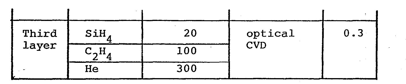
- As described in detail above, since the respective layer are improved in interface characteristics, semiconductor devices with excellent characteristics can be obtained as shown by the above examples.
- Also, the present invention can effect conservation of energy and at the same time can give an electronic device having a deposited film having uniform physical characteristics over a large area with easy management of the film quality. Further, it can give easily an electronic device having a multi-layer structure excellent in physical characteristics such as electrical, optical, semiconductor characteristics, etc., and in productivity and bulk productivity.
Claims (21)
Applications Claiming Priority (2)
| Application Number | Priority Date | Filing Date | Title |
|---|---|---|---|
| JP60298044A JPH0651908B2 (en) | 1985-12-28 | 1985-12-28 | Method of forming thin film multilayer structure |
| JP298044/85 | 1985-12-28 |
Publications (3)
| Publication Number | Publication Date |
|---|---|
| EP0228295A2 true EP0228295A2 (en) | 1987-07-08 |
| EP0228295A3 EP0228295A3 (en) | 1988-11-30 |
| EP0228295B1 EP0228295B1 (en) | 1992-08-26 |
Family
ID=17854397
Family Applications (1)
| Application Number | Title | Priority Date | Filing Date |
|---|---|---|---|
| EP86310163A Expired - Lifetime EP0228295B1 (en) | 1985-12-28 | 1986-12-24 | Method for producing an electronic device having a multi-layer structure |
Country Status (5)
| Country | Link |
|---|---|
| US (1) | US4766091A (en) |
| EP (1) | EP0228295B1 (en) |
| JP (1) | JPH0651908B2 (en) |
| CA (1) | CA1256593A (en) |
| DE (1) | DE3686568T2 (en) |
Cited By (1)
| Publication number | Priority date | Publication date | Assignee | Title |
|---|---|---|---|---|
| EP0231660A3 (en) * | 1985-12-28 | 1988-11-23 | Canon Kabushiki Kaisha | Method for producing an electronic device having a multi-layer structure and electronic device obtained thereby |
Families Citing this family (5)
| Publication number | Priority date | Publication date | Assignee | Title |
|---|---|---|---|---|
| KR910003742B1 (en) * | 1986-09-09 | 1991-06-10 | 세미콘덕터 에너지 라보라터리 캄파니 리미티드 | Cvd apparatus |
| US5229081A (en) * | 1988-02-12 | 1993-07-20 | Regal Joint Co., Ltd. | Apparatus for semiconductor process including photo-excitation process |
| EP0410390A3 (en) * | 1989-07-27 | 1993-02-24 | Seiko Instruments Inc. | Method of producing semiconductor device |
| CA2718253C (en) * | 2008-03-12 | 2016-04-19 | Ricardo Enrique Biana | Plasma system |
| US20220367216A1 (en) * | 2021-05-11 | 2022-11-17 | Applied Materials, Inc. | Multi-zone lamp heating and temperature monitoring in epitaxy process chamber |
Family Cites Families (33)
| Publication number | Priority date | Publication date | Assignee | Title |
|---|---|---|---|---|
| US31708A (en) * | 1861-03-19 | Improved device for coating pins | ||
| US3473978A (en) * | 1967-04-24 | 1969-10-21 | Motorola Inc | Epitaxial growth of germanium |
| US3888705A (en) * | 1973-12-19 | 1975-06-10 | Nasa | Vapor phase growth of groups iii-v compounds by hydrogen chloride transport of the elements |
| USRE31708E (en) | 1976-11-01 | 1984-10-16 | Method of depositing electrically conductive, infra-red reflective, transparent coatings of stannic oxide | |
| US4146657A (en) * | 1976-11-01 | 1979-03-27 | Gordon Roy G | Method of depositing electrically conductive, infra-red reflective, transparent coatings of stannic oxide |
| GB2038086A (en) * | 1978-12-19 | 1980-07-16 | Standard Telephones Cables Ltd | Amorphous semiconductor devices |
| US4239811A (en) * | 1979-08-16 | 1980-12-16 | International Business Machines Corporation | Low pressure chemical vapor deposition of silicon dioxide with oxygen enhancement of the chlorosilane-nitrous oxide reaction |
| JPS5710920A (en) * | 1980-06-23 | 1982-01-20 | Canon Inc | Film forming process |
| US4522663A (en) * | 1980-09-09 | 1985-06-11 | Sovonics Solar Systems | Method for optimizing photoresponsive amorphous alloys and devices |
| KR890004497B1 (en) * | 1980-09-09 | 1989-11-06 | 에너지 컨버션 디바이시즈, 인코포레이티드 | Method for optimizing photoresponsive amorphous alloys and devices |
| US4357179A (en) * | 1980-12-23 | 1982-11-02 | Bell Telephone Laboratories, Incorporated | Method for producing devices comprising high density amorphous silicon or germanium layers by low pressure CVD technique |
| US4459163A (en) * | 1981-03-11 | 1984-07-10 | Chronar Corporation | Amorphous semiconductor method |
| US4421592A (en) * | 1981-05-22 | 1983-12-20 | United Technologies Corporation | Plasma enhanced deposition of semiconductors |
| US4402762A (en) * | 1981-06-02 | 1983-09-06 | John Puthenveetil K | Method of making highly stable modified amorphous silicon and germanium films |
| JPS5833829A (en) * | 1981-08-24 | 1983-02-28 | Toshiba Corp | Thin film forming apparatus |
| US4652463A (en) * | 1982-03-29 | 1987-03-24 | Hughes Aircraft | Process for depositing a conductive oxide layer |
| JPS58170536A (en) * | 1982-03-31 | 1983-10-07 | Fujitsu Ltd | Plasma treating method and apparatus therefor |
| US4462847A (en) * | 1982-06-21 | 1984-07-31 | Texas Instruments Incorporated | Fabrication of dielectrically isolated microelectronic semiconductor circuits utilizing selective growth by low pressure vapor deposition |
| US4504518A (en) * | 1982-09-24 | 1985-03-12 | Energy Conversion Devices, Inc. | Method of making amorphous semiconductor alloys and devices using microwave energy |
| US4615905A (en) * | 1982-09-24 | 1986-10-07 | Sovonics Solar Systems, Inc. | Method of depositing semiconductor films by free radical generation |
| JPS59159167A (en) * | 1983-03-01 | 1984-09-08 | Zenko Hirose | Manufacture of amorphous silicon film |
| JPS59199035A (en) * | 1983-04-26 | 1984-11-12 | Fuji Electric Corp Res & Dev Ltd | Device for forming thin film |
| JPS6026664A (en) * | 1983-07-22 | 1985-02-09 | Canon Inc | Formation of deposited amorphous silicon film |
| DE3429899A1 (en) * | 1983-08-16 | 1985-03-07 | Canon K.K., Tokio/Tokyo | METHOD FOR FORMING A DEPOSITION FILM |
| US4637938A (en) * | 1983-08-19 | 1987-01-20 | Energy Conversion Devices, Inc. | Methods of using selective optical excitation in deposition processes and the detection of new compositions |
| JPS6043819A (en) * | 1983-08-19 | 1985-03-08 | Semiconductor Energy Lab Co Ltd | Method for vapor-phase reaction |
| US4645689A (en) * | 1984-02-17 | 1987-02-24 | At&T Bell Laboratories | Deposition technique |
| JPS60243663A (en) * | 1984-05-18 | 1985-12-03 | Kyocera Corp | Electrophotographic sensitive body |
| US4624736A (en) * | 1984-07-24 | 1986-11-25 | The United States Of America As Represented By The United States Department Of Energy | Laser/plasma chemical processing of substrates |
| US4657777A (en) * | 1984-12-17 | 1987-04-14 | Canon Kabushiki Kaisha | Formation of deposited film |
| JPH07101751B2 (en) * | 1985-03-28 | 1995-11-01 | キヤノン株式会社 | Photovoltaic device manufacturing method |
| US4719123A (en) * | 1985-08-05 | 1988-01-12 | Sanyo Electric Co., Ltd. | Method for fabricating periodically multilayered film |
| JP2566914B2 (en) * | 1985-12-28 | 1996-12-25 | キヤノン株式会社 | Thin film semiconductor device and method of forming the same |
-
1985
- 1985-12-28 JP JP60298044A patent/JPH0651908B2/en not_active Expired - Lifetime
-
1986
- 1986-12-24 EP EP86310163A patent/EP0228295B1/en not_active Expired - Lifetime
- 1986-12-24 CA CA000526326A patent/CA1256593A/en not_active Expired
- 1986-12-24 DE DE8686310163T patent/DE3686568T2/en not_active Expired - Lifetime
- 1986-12-24 US US06/946,085 patent/US4766091A/en not_active Expired - Lifetime
Cited By (1)
| Publication number | Priority date | Publication date | Assignee | Title |
|---|---|---|---|---|
| EP0231660A3 (en) * | 1985-12-28 | 1988-11-23 | Canon Kabushiki Kaisha | Method for producing an electronic device having a multi-layer structure and electronic device obtained thereby |
Also Published As
| Publication number | Publication date |
|---|---|
| JPS62158873A (en) | 1987-07-14 |
| JPH0651908B2 (en) | 1994-07-06 |
| DE3686568D1 (en) | 1992-10-01 |
| EP0228295A3 (en) | 1988-11-30 |
| CA1256593A (en) | 1989-06-27 |
| EP0228295B1 (en) | 1992-08-26 |
| US4766091A (en) | 1988-08-23 |
| DE3686568T2 (en) | 1993-01-21 |
Similar Documents
| Publication | Publication Date | Title |
|---|---|---|
| US4771015A (en) | Method for producing an electronic device having a multi-layer structure | |
| CA1257403A (en) | Chemical vapour deposition method to produce an electronic device having a multi-layer structure | |
| US4683146A (en) | Process for producing deposition films | |
| US4812325A (en) | Method for forming a deposited film | |
| US4868014A (en) | Method for forming thin film multi-layer structure member | |
| US5160543A (en) | Device for forming a deposited film | |
| US4812328A (en) | Method for forming deposited film | |
| US4772570A (en) | Method for producing an electronic device having a multi-layer structure | |
| US5470389A (en) | Apparatus for forming deposited film | |
| US4801474A (en) | Method for forming thin film multi-layer structure member | |
| US4822636A (en) | Method for forming deposited film | |
| EP0234094B1 (en) | Method for forming deposited film | |
| US4766091A (en) | Method for producing an electronic device having a multi-layer structure | |
| EP0264505B1 (en) | Method for forming a deposited film | |
| US4826778A (en) | Process for the preparation of a PIN opto-electric conversion element | |
| EP0228910B1 (en) | Apparatus for forming deposited film | |
| JP2637397B2 (en) | Deposition film formation method | |
| JP2547728B2 (en) | Deposition film forming equipment | |
| JPH0645895B2 (en) | Deposited film forming equipment | |
| JPH0647729B2 (en) | Deposited film formation method | |
| JPH0645884B2 (en) | Deposited film formation method | |
| JPH084069B2 (en) | Thin film semiconductor device and method of forming the same |
Legal Events
| Date | Code | Title | Description |
|---|---|---|---|
| PUAI | Public reference made under article 153(3) epc to a published international application that has entered the european phase |
Free format text: ORIGINAL CODE: 0009012 |
|
| AK | Designated contracting states |
Kind code of ref document: A2 Designated state(s): DE FR GB IT NL |
|
| PUAL | Search report despatched |
Free format text: ORIGINAL CODE: 0009013 |
|
| AK | Designated contracting states |
Kind code of ref document: A3 Designated state(s): DE FR GB IT NL |
|
| 17P | Request for examination filed |
Effective date: 19890419 |
|
| 17Q | First examination report despatched |
Effective date: 19900206 |
|
| GRAA | (expected) grant |
Free format text: ORIGINAL CODE: 0009210 |
|
| AK | Designated contracting states |
Kind code of ref document: B1 Designated state(s): DE FR GB IT NL |
|
| PG25 | Lapsed in a contracting state [announced via postgrant information from national office to epo] |
Ref country code: NL Effective date: 19920826 |
|
| REF | Corresponds to: |
Ref document number: 3686568 Country of ref document: DE Date of ref document: 19921001 |
|
| ET | Fr: translation filed | ||
| ITF | It: translation for a ep patent filed | ||
| NLV1 | Nl: lapsed or annulled due to failure to fulfill the requirements of art. 29p and 29m of the patents act | ||
| PLBE | No opposition filed within time limit |
Free format text: ORIGINAL CODE: 0009261 |
|
| STAA | Information on the status of an ep patent application or granted ep patent |
Free format text: STATUS: NO OPPOSITION FILED WITHIN TIME LIMIT |
|
| 26N | No opposition filed | ||
| ITTA | It: last paid annual fee | ||
| REG | Reference to a national code |
Ref country code: GB Ref legal event code: IF02 |
|
| PGFP | Annual fee paid to national office [announced via postgrant information from national office to epo] |
Ref country code: GB Payment date: 20051212 Year of fee payment: 20 |
|
| PGFP | Annual fee paid to national office [announced via postgrant information from national office to epo] |
Ref country code: FR Payment date: 20051216 Year of fee payment: 20 |
|
| PGFP | Annual fee paid to national office [announced via postgrant information from national office to epo] |
Ref country code: IT Payment date: 20051228 Year of fee payment: 20 |
|
| PGFP | Annual fee paid to national office [announced via postgrant information from national office to epo] |
Ref country code: DE Payment date: 20060224 Year of fee payment: 20 |
|
| PG25 | Lapsed in a contracting state [announced via postgrant information from national office to epo] |
Ref country code: GB Free format text: LAPSE BECAUSE OF EXPIRATION OF PROTECTION Effective date: 20061223 |
|
| REG | Reference to a national code |
Ref country code: GB Ref legal event code: PE20 |