EP0228329B1 - Einen schnellen stabilen Speicher bildende elektronische Vorrichtung - Google Patents
Einen schnellen stabilen Speicher bildende elektronische Vorrichtung Download PDFInfo
- Publication number
- EP0228329B1 EP0228329B1 EP86402736A EP86402736A EP0228329B1 EP 0228329 B1 EP0228329 B1 EP 0228329B1 EP 86402736 A EP86402736 A EP 86402736A EP 86402736 A EP86402736 A EP 86402736A EP 0228329 B1 EP0228329 B1 EP 0228329B1
- Authority
- EP
- European Patent Office
- Prior art keywords
- memory
- state
- access
- logic controller
- address
- Prior art date
- Legal status (The legal status is an assumption and is not a legal conclusion. Google has not performed a legal analysis and makes no representation as to the accuracy of the status listed.)
- Expired - Lifetime
Links
Images


Classifications
-
- G—PHYSICS
- G06—COMPUTING OR CALCULATING; COUNTING
- G06F—ELECTRIC DIGITAL DATA PROCESSING
- G06F12/00—Accessing, addressing or allocating within memory systems or architectures
- G06F12/02—Addressing or allocation; Relocation
- G06F12/0223—User address space allocation, e.g. contiguous or non contiguous base addressing
- G06F12/023—Free address space management
-
- G—PHYSICS
- G06—COMPUTING OR CALCULATING; COUNTING
- G06F—ELECTRIC DIGITAL DATA PROCESSING
- G06F12/00—Accessing, addressing or allocating within memory systems or architectures
- G06F12/14—Protection against unauthorised use of memory or access to memory
- G06F12/1416—Protection against unauthorised use of memory or access to memory by checking the object accessibility, e.g. type of access defined by the memory independently of subject rights
- G06F12/1425—Protection against unauthorised use of memory or access to memory by checking the object accessibility, e.g. type of access defined by the memory independently of subject rights the protection being physical, e.g. cell, word, block
Definitions
- the invention relates to electronic memories.
- the present invention improves the previous fast stable memory, in order to remedy these drawbacks.
- a first aim of the present invention is to ensure that the atomicity of the operations performed by the stable memory practically no longer rests on the user processor, and this in particular for the mutual exclusion, copying, and creation mechanisms. memory areas, as will be seen later in detail.
- Another object of the invention is that the size of the protected memory areas is no longer linked to the hardware structure of the memory; we will thus define an object, which is a subset of memory words, contiguous or not.
- an object can be broken down into sub-objects, which are groups of memory areas, contiguous or not, but necessarily included in the memory part relating to the object to which they are attached.
- Yet another object of the present invention is to provide a stable memory whose speed is greater than previously.
- the invention starts from a fast stable memory, comprising address interfaces, data input / output and write and read instructions, capable of being directly connected to a processor.
- external, first and second independent sets of non-volatile random access memory having address inputs, write / read control inputs, and data inputs / outputs, and access control means connected to on the one hand to the address and write / read command interfaces, on the other hand to the address and write / read command inputs of the two sets of memory, so as not to authorize the access only to a designated part of the two memory sets, each time for a designated read or write operation, the authorization being destroyed after the addressing of this memory part.
- the access control means comprise a logic controller, associated with a first non-volatile auxiliary memory, intended to contain partition information capable of decomposing identically each of the memory sets according to at least one level of sub- disjoint sets, said objects; and the logic controller decomposes each request for access to memory by the external processor into one or more active access states, in each of which it verifies that the series of addresses applied to the memory sets covers a subset (or object ) complete, as defined by the partition information, any anomaly resulting in the logic controller going into an error state.
- the memory includes a switching member having at least one transfer state where it interconnects the inputs / outputs of the first memory assembly with the data input / output interface, and an exchange state where it interconnects the data inputs / outputs of the two memory sets; for its part, the logic controller has a free state, where it can receive a write or read command of the external processor, an active read state, accessible directly from the free state in response to a read command, an active write state in one of the memory sets where it places the switch body in its transfer state, an active state of copying one into the other of the memory assemblies, where it places the switch body in its exchange state, as well as at least one state of error, the execution of a write command from the external processor implying passage through the write state, then through the copy state, before any return to the free state.
- a second auxiliary memory living and non-volatile, forming a marking vector, of the same size as the memory sets, addressed like them, and each component of which, in its normal state, prohibits access for alteration to words having the address associated with this component, in either of these two sets of memory; in response to a write command from the external processor, the logic controller activates the marking vector before writing to the first memory set, selectively for the sequence of addresses requested, which it checks according to said partition information, then returns the marking vector to its normal state after the copying of the first set of memory into the second, any anomaly resulting in the passage of the logic controller into an error state.
- the switch member also has a state of comparison of the respective data outputs of the two memory sets, to indicate their agreement to the logic controller.
- the switching device in its state of comparison, can carry out a prior check of the respective outputs of the two memory sets, in order to determine possible altered bits there.
- the execution of a write instruction comprises passing through an active open state ("read update") during which all the words making up the subset to be written are explored, and during which s '' performs, for each of these words, the change of state of the marking vector, and the comparison state is implemented by the logic controller during this active opening state, which allows a control of the content, in particular consistency, of the object by the processor, before the actual writing.
- read update an active open state
- the logic controller authorizes the simultaneous reading of the two memory sets, the value read being validated only if there is a match between the data outputs of the two memory sets.
- the logic controller has another state, called object creation, allowing the processor to define said partition information, with the logic controller, and yet another state, said object destruction, allowing to modify the partitions existing in the memory, in particular to delete the locations of objects which have become useless.
- the partition information includes chaining information between the addresses of the words of the memory sets, and at least one set of pointing information on the addresses of the first and of the last word of each subset (object), or better still, the partition information comprises at least one other set of pointing information making it possible to define in each subset (object) at least one other level of subsets (sub-objects).
- the memory comprises a command register, in RAM and non-volatile memory, receiving alone both the addresses and the data of the external processor, by which it is directly addressable, and capable of containing a command in progress, as well as an access level in the partition.
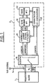
- a processor or a processing unit card comprising a processor, denoted 1 is connected on the one hand to a local bus 10, on the other hand to a global bus 16, which it can share with other analog processors.
- the interface 30 is provided with a switching whose normal state means that the processor 1 communicates by the local bus 10 with the memory 2. However, when the processor 1 is inactive or unavailable, the other state allows the connection of the memory 2 by the interface 30 on the global bus 16, hence the ability to share fast stable memory between multiple processors.
- the stable memory 2 comprises, in addition to the interface 30 already mentioned, a logic access controller or filter 20, two sets of memory 51 and 52, which will be called more briefly memory banks (note being made that the word “ bench “does not have the same definition here as in the previous patent application), and a distributor member 40.
- the latter is advantageously also provided with a comparator.
- the addresses and commands drawn by the interface 30 of the local bus 10 are transmitted to the access logic controller 20, which, under condition, transmits them to the memory banks 51 and 52, while simultaneously controlling the state of the distributor 40 .
- the data drawn by the interface 30 of the local bus 10 are sent directly to the distributor 40, which can make various connections of this data to the memory banks 51 and 52.
- the access logic controller or filter 20 is associated with an auxiliary memory, living and non-volatile, intended to contain information defining an identical partition of two sets of memory according to at least one level of disjoint subsets , which we will now call objects.
- This information can be recorded in the form of a vector memory, of the same size as the two memory banks 51 and 52.
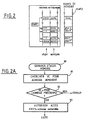
- chaining vector VC the general role of which will now be described with reference to FIG. 2A.
- a function 81 examines the content of the chaining vector VC at this address. The address of the memory word previously requested has been stored in the PMOT register. Function 82 determines whether the content of VC is the same as PMOT, before authorizing memory access (83), and putting the new address in PMOT. This process is repeated, until it traverses the whole object.
- access to the memory is prohibited for words that do not belong to any object.
- the chaining vector is then initialized with a value that cannot be interpreted as a pointer, which causes an error during access.
- the chaining vector makes it possible to ensure the atomicity of an operation on an object, and to avoid any overlap between two memory areas belonging to two different objects.
- the logic controller verifies that the series of addresses requested by the external processor covers a subset or complete object, as defined by the corresponding partition information of the chaining vector.
- the logic controller 20 also uses a marking vector, which also has the same size as each of the memory banks 51 and 52. This marking vector can, in each position, include a single bit. The normal value, zero for example, prohibits access for alteration to the word which has the address associated with this bit (which is a component of the marking vector) in one and the other of the two memory banks 51 and 52. On the contrary, the active value 1 authorizes such access.
- the logic controller 20 activates the marking vector before writing to the first memory bank 51. This activation selectively concerns only the components of the marking vector which correspond to the sequence of addresses requested by the external processor. At the same time, verification is made that the series of addresses requested by the external processor covers a complete object or sub-object, as defined by the chaining vector or vectors.
- the marking vector is returned to its normal state (for the components concerned) only after the copying of the first memory bank 51 into the second 52. Any anomaly results in the passage of the logic controller 20 in an error state .
- the activation of the marking vector can take place during the active writing state itself, but of course before the actual writing action. There is indeed security, because the previous content of the object remains entirely contained in the second memory bank 52, as long as the writing in the first bank 51 is not completed.
- the execution of a write instruction comprises first of all the passage of the logic controller 20 through an active opening state (also called "read update") during which all the words making up the object or sub-object to be written are explored, and during which the state of the marking vector is changed for each of these words, preferably after having verified by joint reading of the two memory banks that their contents (relative to the previous version of the object) coincide.
- an active opening state also called "read update”
- the execution of the writing instruction then continues by passing into the active writing state (without touching the marking vector) and then into the active copying state, during which each copying operation is followed. a return of the marking vector to its normal state, for each of the memory words concerned.
- the execution of a read instruction can be done in the same way as the active state of opening or updating read already mentioned, except the very important fact that one omits to modify the marking vector, which thus remains in its normal state prohibiting any modification of the memory banks 51 and 52.
- the reading is accompanied by a comparison of the contents of the two memory banks, before the information read is delivered to the external processor through the interface 30.
- the distributor member (or switch) is also arranged to perform a prior check of the respective outputs of the two memory banks, in order to determine possible altered bits ("decay" of the memory ), by any known error detection code, in particular parity check. It is then possible to update one of the memory banks (the one whose bits are corrupted) relative to the other.
- the logic controller has another state, called "creation of objects", allowing the external processor to define in advance the partition information, that is to say the chaining vectors, under the logic controller control.
- this other state allows the external processor to dynamically modify the partitions existing in the memory.
- the invention allows the logic controller to define a new object from existing objects (which become sub-objects) or vice versa to define new sub-objects of an existing object; in both cases, the contents of the objects can be preserved.
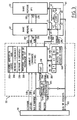
- FIG. 3 illustrates in more detail the stable memory card, in this particular example.
- the interface 30 decomposes the local bus (or the global bus) into a data bus 300, into an address bus 310, if necessary into a write line 320 and a read line 330 (signals directly interpretable by memory banks 51 and 52), and also in lines 340 and 350 which can respectively carry a general reset signal denoted RAZGEN (or "reset"), and a reset signal after error denoted RAZERR.
- RAZGEN general reset signal
- RAZERR reset signal after error denoted RAZERR.
- control logic 200 is in practice produced in wired form, for example using programmable logic arrays, rather than by microprocessors.
- a register 205 receives the address bus 310 and the data bus 300, in order to be able to store the commands coming from the external processor. These commands are supplied to it directly, since this register has a particular address, seen from the external processor.
- the dialogue of this register 205 with the control logic 200 essentially consists of the transfer of the command into the STATUS register 210, when the logic 200 authorizes it, by a line 206.
- a line 208 allows the logic to command 200 to send an error signal to the processor control register 205. This error signal can then be read by the external processor.
- a member 260 allows the calculation of a coding function which will be defined later, using memories 235 and 245.
- the connections of the logic access controller 20 to the memory banks 51 and 52 are limited to the transfer of the same address information to them, as well as to the transfer (this time selective) of the write control signals and read which are suitable for these memory banks 51 and 52.
- the address bus is denoted 270.
- the write commands are denoted 281 and 282 respectively for benches 51 and 52.
- the read commands are denoted 291 and 292 , respectively for banks 51 and 52.
- the data inputs and outputs of bank 51 are on a bus 41.
- Those of bank 52 are on a bus 42.
- the two buses can be interconnected by a switch 43 of switch 40 (switch 43 is closed in the exchange status of the switch).
- the buses 41 and 42 can be applied on either side of a comparator 44 by switches 45 and 46, both closed in the comparison state of the distributor 40.
- Another switch 47 allows the connection of the bus 41 to the data bus 300. It may be useful to also provide a switch 48 to connect the buses 42 and 300.
- the state of the switches 43 to 47 (if applicable 48) is under the control of the switch control signals denoted CDIS, and coming from lines 290 of the logic controller 20.
- the comparator 44 may indicate a comparison error , via a line 295, to the access logic controller 20.
- the fast stable memory of FIG. 3 is implemented by a random access memory card, backed up by battery, and directly addressable by the external processor, through the interface. 30 which is satisfied with making interconnections and, where appropriate, switching between the local bus and the global bus, already described with reference to FIG. 1.
- the only element of the stable memory card that can be directly addressed to the external processor is the command register 205.
- the processor will therefore be able to put COMMANDS there, the list of which (for this particular example) is given in appendix A2, and the level N concerned.
- the COMMAND determines the possibilities of access to the memory banks 51 and 52 (B1 and B2 in Appendix A2).
- Each FUNCTION will be associated with a FUNCTION (which in principle has the same name).
- the FUNCTION is executed each time the external processor presents a new address on the address bus 310. This address is either accompanied by a word on hold (if it is a read), or accompanied by 'a real word (if it is a writing), or accompanied by an empty word (especially when memory will copy the first bank into the second).
- the vector memories B and C (denoted 230 and 240) cannot be addressed by the external processor.
- Each box or component of the vector that constitutes the memory B consists of a couple of two bits.
- the first bit is set to 1 if the address of the couple in memory B corresponds to the address of the first word of an object (or sub-object, etc.) in the memory banks 51 and 52.
- the second bit is to 1 if it is the last word of an object (sub-object, etc.).
- the two bits are 0 in the other cases.
- each box or address of the vector memory B contains as many pairs of bits as there are possible levels of objects and sub-objects.
- the vector memory C could be produced in the form of an array of pointers which links all the words individually constituting an object (and therefore its sub-objects, etc.). However, these vector memories necessarily have the same address size (that is to say the same number of boxes) as banks 51 and 52. If banks 51 and 52 have a megamot or a megamultiplet (for example a megabyte), an address contains 20 bits.
- This coding consists in storing in the chaining vector C (memory 240) the sum of the number of bits at 1 of the pointer and the number of bits at 1 of the content of the vector memory C for the preceding word, that is to say say the one designated by this pointer.
- any second word receives as value C the number of bits at 1 of the address of the first word.
- the register P noted 218 will have made it possible to indicate whether or not it is the first word of an object (and of an object only, not of a sub-object).
- the register BI has the same size as a box in the vector memory B. This register BI therefore stores, for each level, a pair of bits indicating whether one is at the first word of an object (or sub-object, etc.), during the object (or sub-object, etc.), or at the last word of an object (or sub-object, etc.).
- the part of BI that must be taken into account is defined by the value of N contained in register 215.
- the content of the BI register is reset to zero at the start of each phase of a memory access. If during an access, a terminal is encountered, it is registered in BI.
- BliNI At the end of an access phase to an object or sub-object, BliNI must be equal to (1,1).
- the structure of the marking vector VP contained in the memory 220 is simpler, since this time there is only one bit for each possible address in the memory banks 51 and 52. This bit is nominally at zero, for prohibit access to memory banks in order to modify their content. When it is on the contrary to 1, it is possible to modify the content of the memory banks, at the corresponding address.
- the current address, noted moti, is contained in register 250.
- FIG. 3A takes up a part of the elements of FIG. 3, in a different illustration which makes it possible to better understand the close link between the hardware structure of the stable memory, and the functions described below.
- logic gates 321 to 323 (AND gates) as well as 324 to 327 (OR gates) to obtain the mutual exclusion of the two writing banks.
- logic gates 321 to 323 (AND gates)
- 324 to 327 OR gates
- ET gates 328 and 329 allow reading
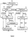
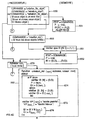
- the starting point is free state 100.
- the processor delivers a READ COMMAND, accompanied by the appropriate access level N.
- the memory performs an initialization step after command, consisting first of all in writing the command in question in its state register 210, then in passing the contents P of its first register 218 to TRUE. word, finally to reset to zero all the levels of the BI content of its current terminal register 235.
- Step 412 then consists in arming the watchdog for the appropriate time delay.
- the processor transmits in 413 the address of a word that it wants to read. It will be understood that the addresses presented must sequentially cover all the words constituting the object considered. A reading FUNCTION 400 is then started in the memory, repeated for each address presented in 413.
- steps 414 allow the chaining control, this expression now also including the control of the bounds.
- step 415 consists in verifying that the two words contained in the banks B1 and B2 at the word address; are equal, in which case we take one of them, for example B1 (moti). Otherwise, it is a fatal error and we go to state 150 of FIG. 4.
- step 416 which consists of incrementing the chaining, first of all by performing the operation of EXTENDED OR on BI, then by determining the new value of the chaining indicator CI.
- step 418 the memory first checks that the last limit has indeed been reached for BI (N). She then agrees to go to the fiber state, then disarms her watchdog in 419.
- step 411 illustrated in isolation in FIG. 4B with its designation "initialization after command”.
- step 414 illustrated in the same way in FIG. 4C with its designation "chaining control".
- step 416 illustrated in FIG. 4D with its designation "chaining incrementation”.
- step 418 illustrated in FIG. 4E with its designation "front control" free "".
- FIGS. 5, 5A and 5B for the description of the writing, which is certainly one of the most important aspects of the invention.
- the processor delivers an update-read COMMAND, as well as the access level N.
- the memory responds in 512 by initialization after command (FIG. 4B), then arms the watchdog in 513 at a predetermined value, which may be different from that of the reading.
- the processor will repeatedly deliver the address of a word, as for reading.
- steps 515, 517 and 518 are identical to steps 414, 415 and 416, respectively.
- the processor issues at 520 a write update COMMAND.
- the stable memory responds to it in 521 by verifying that the last bound of the object or sub-object has indeed been reached during the previous reading update procedure. Then, it performs, in 522, an initialization after command (FIG. 4B).
- the processor then repeatedly delivers, at 523, an address and the value of a word to be written to this address.
- the memory responds with the write-update FUNCTION 502.
- This procedure again includes a chaining check 524 (FIG. 4C).
- the memory checks, in 525, that the protection vector is "access permitted" for the word address; presented by the processor.
- Step 527 is then the chaining increment of FIG. 4D.
- the processor issues in 528 an UPDATE update command.
- the memory responds to it as before by checking in 529 that the write update step has gone to the last terminal of the object or sub-object. It then performs, in 530, the initialization after command of FIG. 4B.
- the processor then presents, at 531, a word address; accompanied by any word (it involves writing the memoirs, but the word presented is not significant). This is of course repeated as before.
- the memory performs the updated copying FUNCTION 503, which begins at 532 with the chaining check in FIG. 4C.
- the actual copying takes place in 533, by writing into the bank B2, at the word address i , the content of the bank B1, which we have just written at the same word address.
- the memory performs, in 534, the chaining incrementation of FIG. 4D, then, in 535, it verifies that the protection vector for the address moti was indeed “allowed access”, after which it passes it to "access prohibited”.
- the processor delivers in 536 the command "free".
- the memory responds to this, in 537, by carrying out the "free" front control of FIG. 4E, then disarms the watchdog in 538.
- Another simplified writing mode is possible, in particular when the content of an object is first written (the memory of which therefore has no previous version).
- partition information namely the bounds and the chaining vector, could be entered once and for all by construction, or even be revisable by special procedures, but very cumbersome.
- the first intervention of the processor, noted 611, is an access level N, accompanied by a COMMAND which is "object creation” if it is an object with several words, or "creation-end- object "if it is a single word object.
- the memory responds to it with a step 612 which is again the initialization after command of FIG. 4B, followed in 613 by the arming of the watchdog.
- the memory responds with a FUNCTION 601 for creating an object.
- step 617 places a corresponding terminal in the terminal vector B, at the word address and at the level N concerned, then sets P to FALSE.
- step 617 initializes the chaining indicator CI to zero.
- step 618 gives this chaining indicator the value already established for the vector C, at the word address;, at the first level where N was equal to 1.
- step 619 verifies that a first terminal has been placed on the upper level.
- step 620 verifies that the value of the chaining vector C at the address moti is a "free word", that is to say that it has not yet is the subject of no registration, after which it is given the value of the chaining indicator CI.
- step 621 verifies that the chaining previously established at the first level is respected.
- Step 622 then performs the chaining increment of FIG. 4D. After that, step 623 places the protection vector at "access allowed" for the address moti.
- the processor delivers in 630 the COMMAND "creation-end-object". We were able to come here directly if it was a single-word object or sub-object.
- the memory simply responds to it at 631 by passing this command into the status register.
- the processor delivers, in 632, the address of this last word.
- the memory responds with a FUNCTION 602 ( Figure 6) called "creation-end-object”.
- Step 636 is the same as step 616.
- Step 637 differs from step 617 in that an end terminal is placed in vector B.
- Steps 638 and 638A are identical to steps 618 and 618A.
- step 639 simply places an end bound in vector B.
- Step 639A is identical to the step of Figure 6A.
- step 640 is identical to step 620, step 641 to step 621, and step 642 corresponds to the meeting of steps 622 and 623, with suppression of the updating of the chaining indicator, useless for a last word.
- a step 643 examines whether one is at the first level, and whether it is the first and the last. word of the first level, in which case the current terminal register BI is reset to zero, and the state "creation-RESET" is established.
- an inter-object (inter-object) state is established in 606, which corresponds (FIG. 6) to the case where one is at a level of sub-object, other sub-objects being to be defined. .
- This state is only a transient state, which will be followed either by the creation of other sub-objects, or by a transition to creation-RESET.
- step 650 defines the COMMAND creation-object or creation-end-object, if the following sub-object has only one word.
- the sequence in 651 consists of a phase close to initialization after command in FIG. 4B, except that the last line only resets to zero the part of the register BI which corresponds to the level N where we are (with N different from 1). Then, we return to (2), that is to say to step 615.
- Step 660 consists in generating the CREATE-RESET COMMAND for a sub-object.
- the memory verifies that the last limit of the upper level has been reached, that is to say that the last sub-object of the current level has indeed been created.
- step 670 which it has also been able to access since 650.
- the processor will therefore present the moti addresses of all the words.
- Step 675 then verifies that the marking vector VP was indeed "access permitted", to immediately change it to "access prohibited".
- Step 676 is now the chaining increment of Figure 4D.
- step 680 the processor must now present the creation-RESET command again, at least if there are non-validated sub-objects. Otherwise, you can go directly to step 690.
- Step 681 consists in verifying that, for this sub-object, we have passed from the first terminal to the last terminal.
- Step 682 verifies that the first terminal has been placed on the upper level, and not the last.
- step 632 takes into account the command in the status register
- step 684 changes the register P to TRUE
- step 685 resets the register BI, at the current address, to zero for level N concerned only.
- step 686 returns to step 670, that is to say in (7).
- the memory responds to this by checking that the two bounds have been set for the current level, in step 691. If we were at a level other than the first (that of objects, it checks that it was even at the previous level (s), at step 692.
- the object destruction mechanism which can be described with reference to Figure 7, is relatively simpler.
- phase 701 of destruction-reading comparable to the update-reading 501
- phase 702 of destruction proper comparable to the update-writing 502.
- the FUNCTION destruction-read itself is exactly identical to the FUNCTION read-update 501 (fig.5A).
- step 525 After having, in an equivalent of step 525, verified that the marking vector VP is at "access permitted", it is immediately changed to "access prohibited".
- the writing step 526 is of course skipped, and we pass directly to the chaining increment 527.
- the first is the initialization of the memory, illustrated at 480 in FIG. 4.
- a mechanism error can occur during the actual read 400. This is different from the fact that we obtain two mismatched readings in the two banks, and which leads to fatal error 150.
- an error can occur during the reading update phase 501.
- Activating RAZERR allows you to go to state 571 for processing the opening error.
- This processing is very simple, since it suffices to explore all of the addresses moti in the memory, and to pass for each the marking vector VP to "access prohibited".
- the processor For each moti address, the processor does nothing if the VP marking vector is prohibited access; otherwise, it commands the writing at the current address, in bank B1, of the word already contained in bank B2. After that, the VP marking vector is reset to "access prohibited" for the word address i .
- an error state 576 can occur during the update copy 503.
- processing 577 of this recopy error is the same as in state 574, except that it is here bank B2 that we will copy into bank B1, at each word address; for which the VP labeling vector was "access permitted".
- the VP marking vector is reset to "access prohibited" for the word address;, and so on.
- This processing simply consists in traversing all the words of the memory, by putting back the vector of VP (moti) marking with "access prohibited", each time it is "access permitted”. More simply, it is possible to carry out a total reset to zero of the marking vector VP.
- the reading gives two different words on the two memory bands, what is called a mismatched reading.
- the second is to arrive at an error during the recovery, that is to say the processing of a normal error.
- the user processor can determine the correct version of the data by software checks, and that it is therefore the processor itself which gives the order of general reset.
- the same memory can also be managed by stable zones, of fixed size. This can be done, for example, by positioning a switch on the card. Error handling will be the same as for normal mode.
- the first improvement relates to the possibility of authenticating the objects during an update (normal or rapid). This is implemented by comparing the first word of each object with a key stored in a KEY AUTHENT register. This authentication is performed if an AUTHENT register is set to true (value to be determined). Otherwise the update algorithms remain the same.
- the AUTHENT register is writable only in the FREE state.
- the second improvement consists of adding primitives for updating groups of objects (rapid update, or with pre-reading). During the first stage of the update, the objects are marked and counted. In the following steps, we count the number of objects to verify that all the objects have been mdofied.
- the access level of each of the objects may be different from the others. This requires the creation of a BN table, memorizing the level of access to each object. During the first step of the update, the elements of BN corresponding to the first words of the objects are marked with the current access level (N). During the following steps, this level is checked.
Landscapes
- Engineering & Computer Science (AREA)
- Theoretical Computer Science (AREA)
- Physics & Mathematics (AREA)
- General Engineering & Computer Science (AREA)
- General Physics & Mathematics (AREA)
- Computer Security & Cryptography (AREA)
- Storage Device Security (AREA)
- Techniques For Improving Reliability Of Storages (AREA)
- Complex Calculations (AREA)
- Static Random-Access Memory (AREA)
- Input Circuits Of Receivers And Coupling Of Receivers And Audio Equipment (AREA)
- Stabilization Of Oscillater, Synchronisation, Frequency Synthesizers (AREA)
Claims (21)
Priority Applications (1)
| Application Number | Priority Date | Filing Date | Title |
|---|---|---|---|
| AT86402736T ATE54379T1 (de) | 1985-12-12 | 1986-12-09 | Einen schnellen stabilen speicher bildende elektronische vorrichtung. |
Applications Claiming Priority (2)
| Application Number | Priority Date | Filing Date | Title |
|---|---|---|---|
| FR8518437A FR2591775B1 (fr) | 1985-12-12 | 1985-12-12 | Dispositif electronique formant memoire stable rapide perfectionnee |
| FR8518437 | 1985-12-12 |
Publications (2)
| Publication Number | Publication Date |
|---|---|
| EP0228329A1 EP0228329A1 (de) | 1987-07-08 |
| EP0228329B1 true EP0228329B1 (de) | 1990-07-04 |
Family
ID=9325724
Family Applications (1)
| Application Number | Title | Priority Date | Filing Date |
|---|---|---|---|
| EP86402736A Expired - Lifetime EP0228329B1 (de) | 1985-12-12 | 1986-12-09 | Einen schnellen stabilen Speicher bildende elektronische Vorrichtung |
Country Status (8)
| Country | Link |
|---|---|
| US (1) | US4799186A (de) |
| EP (1) | EP0228329B1 (de) |
| JP (1) | JPH0746327B2 (de) |
| AT (1) | ATE54379T1 (de) |
| CA (1) | CA1254666A (de) |
| DE (1) | DE3672466D1 (de) |
| ES (1) | ES2017074B3 (de) |
| FR (1) | FR2591775B1 (de) |
Families Citing this family (13)
| Publication number | Priority date | Publication date | Assignee | Title |
|---|---|---|---|---|
| US5146581A (en) * | 1988-02-24 | 1992-09-08 | Sanyo Electric Co., Ltd. | Subprogram executing data processing system having bank switching control storing in the same address area in each of memory banks |
| IE63461B1 (en) * | 1989-09-11 | 1995-04-19 | Jeremy Owen Jones | Improvements in and relating to stable memory circuits |
| IE911094A1 (en) * | 1991-04-03 | 1992-11-04 | Tolsys Ltd | A Data Processing Method |
| JPH07122864B2 (ja) * | 1991-07-22 | 1995-12-25 | インターナショナル・ビジネス・マシーンズ・コーポレイション | データ処理システム、データ処理システムに使用するインターフエース回路及びデータ・プロセツサ間の通信方法 |
| US6237108B1 (en) * | 1992-10-09 | 2001-05-22 | Fujitsu Limited | Multiprocessor system having redundant shared memory configuration |
| US5596713A (en) * | 1993-12-08 | 1997-01-21 | Zenith Data Systems Corporation | Method to prevent data loss in an electrically erasable read only memory |
| US5446869A (en) * | 1993-12-30 | 1995-08-29 | International Business Machines Corporation | Configuration and RAM/ROM control of PCI extension card residing on MCA adapter card |
| JPH0950405A (ja) * | 1995-08-04 | 1997-02-18 | Fujitsu Ltd | バックアップ機能付き記憶装置および同記憶装置を有する情報処理システム |
| US5959929A (en) * | 1997-12-29 | 1999-09-28 | Micron Technology, Inc. | Method for writing to multiple banks of a memory device |
| US6981069B2 (en) * | 2001-06-25 | 2005-12-27 | International Business Machines Corp. | Compressed data transmission over a plurality of transmission paths |
| JP4496061B2 (ja) * | 2004-11-11 | 2010-07-07 | パナソニック株式会社 | 機密情報処理装置 |
| JP2012164144A (ja) * | 2011-02-07 | 2012-08-30 | Denso Corp | マイクロコンピュータ |
| CN114579083B (zh) * | 2022-05-09 | 2022-08-05 | 上海擎昆信息科技有限公司 | 一种基于矢量处理器的数据处理装置和方法 |
Family Cites Families (2)
| Publication number | Priority date | Publication date | Assignee | Title |
|---|---|---|---|---|
| US4575792A (en) * | 1982-03-31 | 1986-03-11 | Honeywell Information Systems Inc. | Shared interface apparatus for testing the memory sections of a cache unit |
| FR2553541B1 (fr) * | 1983-10-17 | 1992-02-28 | Inst Nat Rech Inf Automat | Dispositif et procede pour le stockage rapide et stable d'informations |
-
1985
- 1985-12-12 FR FR8518437A patent/FR2591775B1/fr not_active Expired
-
1986
- 1986-12-09 ES ES86402736T patent/ES2017074B3/es not_active Expired - Lifetime
- 1986-12-09 EP EP86402736A patent/EP0228329B1/de not_active Expired - Lifetime
- 1986-12-09 DE DE8686402736T patent/DE3672466D1/de not_active Expired - Lifetime
- 1986-12-09 AT AT86402736T patent/ATE54379T1/de active
- 1986-12-11 CA CA000525086A patent/CA1254666A/fr not_active Expired
- 1986-12-12 JP JP61296512A patent/JPH0746327B2/ja not_active Expired - Lifetime
- 1986-12-12 US US06/941,212 patent/US4799186A/en not_active Expired - Fee Related
Also Published As
| Publication number | Publication date |
|---|---|
| CA1254666A (fr) | 1989-05-23 |
| ATE54379T1 (de) | 1990-07-15 |
| EP0228329A1 (de) | 1987-07-08 |
| JPS62217345A (ja) | 1987-09-24 |
| FR2591775A1 (fr) | 1987-06-19 |
| US4799186A (en) | 1989-01-17 |
| DE3672466D1 (de) | 1990-08-09 |
| JPH0746327B2 (ja) | 1995-05-17 |
| FR2591775B1 (fr) | 1988-03-04 |
| ES2017074B3 (es) | 1991-01-01 |
Similar Documents
| Publication | Publication Date | Title |
|---|---|---|
| EP0228329B1 (de) | Einen schnellen stabilen Speicher bildende elektronische Vorrichtung | |
| EP0018889B1 (de) | Verfahren zur Verlängerung der Gültigkeit der Arbeitszone des Speichers eines Datenträgers | |
| EP0540095B1 (de) | Mikroschaltung für eine Chipkarte mit einem geschützten, programmierbaren Speicher | |
| EP0651394B1 (de) | Integrierte Schaltung mit einem geschützten Speicher und geschütztes System das diese integrierte Schaltung verwendet | |
| CA2034002C (fr) | Procede pour verifier l'integrite d'un logiciel ou de donnees, et systeme pour la mise en oeuvre de ce procede | |
| FR2609175A1 (fr) | Carte a circuits integres et systeme pour verifier le bon fonctionnement de la carte | |
| FR2646942A1 (fr) | Carte a circuit integre | |
| FR2661534A1 (fr) | Dispositif et methode de validation d'une carte a memoire. | |
| FR2583540A1 (fr) | Gestion de memoire pour systeme a microprocesseur. | |
| CH627570A5 (fr) | Dispositif de comptabilisation d'unites homogenes predeterminees. | |
| FR2606909A1 (fr) | Systeme de traitement pour un appareil electronique portatif, tel qu'une carte a circuit integre | |
| FR2667171A1 (fr) | Support portable a micro-circuit facilement programmable et procede de programmation de ce micro-circuit. | |
| FR2663142A1 (fr) | Dispositif electronique portable a memoire. | |
| EP3293637A1 (de) | Indexverwaltung in einem flash-speicher | |
| EP0735489A1 (de) | Verfahren zum Schützen nichtflüchtiger Speicherbereiche | |
| EP4180974B1 (de) | Verfahren und system zur verwaltung eines cache-speichers | |
| FR2640783A1 (fr) | Carte a circuit integre et son procede de commande | |
| EP0838053B1 (de) | Verfahren und gerät zur evolution eines programmes in rom | |
| FR2674647A1 (fr) | Appareil formant chequier electronique pour transactions financieres et procede d'utilisation d'un tel appareil. | |
| FR3051574A1 (fr) | Gestion du stockage dans une memoire flash | |
| WO1999000774A9 (fr) | Module de securite comportant des moyens de creation de liens entre des fichiers principaux et des fichiers auxiliaires | |
| EP3246819B1 (de) | Zähler in einem flash-speicher | |
| WO1997040473A1 (fr) | Systeme securise de controle d'acces permettant l'invalidation automatique de cles electroniques volees ou perdues et/ou le transfert d'habilitation a produire des cles | |
| EP0636984B1 (de) | Verfahren und Vorrichtung zur Überwachung der Daten eines Rechners | |
| WO2002041235A2 (fr) | Procede de verification avant activation d'un programme charge dans une carte a puce |
Legal Events
| Date | Code | Title | Description |
|---|---|---|---|
| PUAI | Public reference made under article 153(3) epc to a published international application that has entered the european phase |
Free format text: ORIGINAL CODE: 0009012 |
|
| AK | Designated contracting states |
Kind code of ref document: A1 Designated state(s): AT BE CH DE ES FR GB GR IT LI LU NL SE |
|
| 17P | Request for examination filed |
Effective date: 19870727 |
|
| 17Q | First examination report despatched |
Effective date: 19891013 |
|
| GRAA | (expected) grant |
Free format text: ORIGINAL CODE: 0009210 |
|
| AK | Designated contracting states |
Kind code of ref document: B1 Designated state(s): AT BE CH DE ES FR GB GR IT LI LU NL SE |
|
| PG25 | Lapsed in a contracting state [announced via postgrant information from national office to epo] |
Ref country code: SE Effective date: 19900704 Ref country code: GR Free format text: LAPSE BECAUSE OF FAILURE TO SUBMIT A TRANSLATION OF THE DESCRIPTION OR TO PAY THE FEE WITHIN THE PRESCRIBED TIME-LIMIT Effective date: 19900704 Ref country code: AT Effective date: 19900704 |
|
| REF | Corresponds to: |
Ref document number: 54379 Country of ref document: AT Date of ref document: 19900715 Kind code of ref document: T |
|
| GBT | Gb: translation of ep patent filed (gb section 77(6)(a)/1977) | ||
| REF | Corresponds to: |
Ref document number: 3672466 Country of ref document: DE Date of ref document: 19900809 |
|
| ITF | It: translation for a ep patent filed | ||
| PLBE | No opposition filed within time limit |
Free format text: ORIGINAL CODE: 0009261 |
|
| STAA | Information on the status of an ep patent application or granted ep patent |
Free format text: STATUS: NO OPPOSITION FILED WITHIN TIME LIMIT |
|
| 26N | No opposition filed | ||
| REG | Reference to a national code |
Ref country code: FR Ref legal event code: ST |
|
| ITTA | It: last paid annual fee | ||
| REG | Reference to a national code |
Ref country code: FR Ref legal event code: AR |
|
| REG | Reference to a national code |
Ref country code: FR Ref legal event code: BR |
|
| EPTA | Lu: last paid annual fee | ||
| PGFP | Annual fee paid to national office [announced via postgrant information from national office to epo] |
Ref country code: LU Payment date: 19941201 Year of fee payment: 9 |
|
| PGFP | Annual fee paid to national office [announced via postgrant information from national office to epo] |
Ref country code: FR Payment date: 19941230 Year of fee payment: 9 Ref country code: ES Payment date: 19941230 Year of fee payment: 9 |
|
| PGFP | Annual fee paid to national office [announced via postgrant information from national office to epo] |
Ref country code: NL Payment date: 19941231 Year of fee payment: 9 |
|
| PGFP | Annual fee paid to national office [announced via postgrant information from national office to epo] |
Ref country code: GB Payment date: 19950103 Year of fee payment: 9 |
|
| PGFP | Annual fee paid to national office [announced via postgrant information from national office to epo] |
Ref country code: BE Payment date: 19950111 Year of fee payment: 9 |
|
| PGFP | Annual fee paid to national office [announced via postgrant information from national office to epo] |
Ref country code: DE Payment date: 19950131 Year of fee payment: 9 |
|
| PGFP | Annual fee paid to national office [announced via postgrant information from national office to epo] |
Ref country code: CH Payment date: 19950307 Year of fee payment: 9 |
|
| PG25 | Lapsed in a contracting state [announced via postgrant information from national office to epo] |
Ref country code: LU Free format text: LAPSE BECAUSE OF NON-PAYMENT OF DUE FEES Effective date: 19951209 Ref country code: GB Effective date: 19951209 |
|
| PG25 | Lapsed in a contracting state [announced via postgrant information from national office to epo] |
Ref country code: ES Free format text: LAPSE BECAUSE OF THE APPLICANT RENOUNCES Effective date: 19951211 |
|
| PG25 | Lapsed in a contracting state [announced via postgrant information from national office to epo] |
Ref country code: LI Effective date: 19951231 Ref country code: CH Effective date: 19951231 Ref country code: BE Effective date: 19951231 |
|
| BERE | Be: lapsed |
Owner name: INRIA INSTITUT NATIONAL DE RECHERCHE EN INFORMATI Effective date: 19951231 |
|
| PG25 | Lapsed in a contracting state [announced via postgrant information from national office to epo] |
Ref country code: NL Effective date: 19960701 |
|
| GBPC | Gb: european patent ceased through non-payment of renewal fee |
Effective date: 19951209 |
|
| REG | Reference to a national code |
Ref country code: CH Ref legal event code: PL |
|
| PG25 | Lapsed in a contracting state [announced via postgrant information from national office to epo] |
Ref country code: FR Effective date: 19960830 |
|
| NLV4 | Nl: lapsed or anulled due to non-payment of the annual fee |
Effective date: 19960701 |
|
| PG25 | Lapsed in a contracting state [announced via postgrant information from national office to epo] |
Ref country code: DE Effective date: 19960903 |
|
| REG | Reference to a national code |
Ref country code: FR Ref legal event code: ST |
|
| REG | Reference to a national code |
Ref country code: ES Ref legal event code: FD2A Effective date: 20010402 |
|
| PG25 | Lapsed in a contracting state [announced via postgrant information from national office to epo] |
Ref country code: IT Free format text: LAPSE BECAUSE OF NON-PAYMENT OF DUE FEES;WARNING: LAPSES OF ITALIAN PATENTS WITH EFFECTIVE DATE BEFORE 2007 MAY HAVE OCCURRED AT ANY TIME BEFORE 2007. THE CORRECT EFFECTIVE DATE MAY BE DIFFERENT FROM THE ONE RECORDED. Effective date: 20051209 |