EP0229950A1 - Transformatorloses Netzgerät - Google Patents
Transformatorloses Netzgerät Download PDFInfo
- Publication number
- EP0229950A1 EP0229950A1 EP86116808A EP86116808A EP0229950A1 EP 0229950 A1 EP0229950 A1 EP 0229950A1 EP 86116808 A EP86116808 A EP 86116808A EP 86116808 A EP86116808 A EP 86116808A EP 0229950 A1 EP0229950 A1 EP 0229950A1
- Authority
- EP
- European Patent Office
- Prior art keywords
- transistor
- load
- voltage
- input
- resistor
- Prior art date
- Legal status (The legal status is an assumption and is not a legal conclusion. Google has not performed a legal analysis and makes no representation as to the accuracy of the status listed.)
- Granted
Links
- 239000003990 capacitor Substances 0.000 claims abstract description 11
- 230000000903 blocking effect Effects 0.000 description 2
- 238000010586 diagram Methods 0.000 description 2
- XUIMIQQOPSSXEZ-UHFFFAOYSA-N Silicon Chemical compound [Si] XUIMIQQOPSSXEZ-UHFFFAOYSA-N 0.000 description 1
- 230000001419 dependent effect Effects 0.000 description 1
- 238000009499 grossing Methods 0.000 description 1
- 229910052710 silicon Inorganic materials 0.000 description 1
- 239000010703 silicon Substances 0.000 description 1
- 230000006641 stabilisation Effects 0.000 description 1
- 238000011105 stabilization Methods 0.000 description 1
- 239000003381 stabilizer Substances 0.000 description 1
Images
Classifications
-
- H—ELECTRICITY
- H02—GENERATION; CONVERSION OR DISTRIBUTION OF ELECTRIC POWER
- H02M—APPARATUS FOR CONVERSION BETWEEN AC AND AC, BETWEEN AC AND DC, OR BETWEEN DC AND DC, AND FOR USE WITH MAINS OR SIMILAR POWER SUPPLY SYSTEMS; CONVERSION OF DC OR AC INPUT POWER INTO SURGE OUTPUT POWER; CONTROL OR REGULATION THEREOF
- H02M3/00—Conversion of DC power input into DC power output
- H02M3/02—Conversion of DC power input into DC power output without intermediate conversion into AC
- H02M3/04—Conversion of DC power input into DC power output without intermediate conversion into AC by static converters
- H02M3/10—Conversion of DC power input into DC power output without intermediate conversion into AC by static converters using discharge tubes with control electrode or semiconductor devices with control electrode
- H02M3/145—Conversion of DC power input into DC power output without intermediate conversion into AC by static converters using discharge tubes with control electrode or semiconductor devices with control electrode using devices of a triode or transistor type requiring continuous application of a control signal
- H02M3/155—Conversion of DC power input into DC power output without intermediate conversion into AC by static converters using discharge tubes with control electrode or semiconductor devices with control electrode using devices of a triode or transistor type requiring continuous application of a control signal using semiconductor devices only
- H02M3/156—Conversion of DC power input into DC power output without intermediate conversion into AC by static converters using discharge tubes with control electrode or semiconductor devices with control electrode using devices of a triode or transistor type requiring continuous application of a control signal using semiconductor devices only with automatic control of output voltage or current, e.g. switching regulators
- H02M3/1563—Conversion of DC power input into DC power output without intermediate conversion into AC by static converters using discharge tubes with control electrode or semiconductor devices with control electrode using devices of a triode or transistor type requiring continuous application of a control signal using semiconductor devices only with automatic control of output voltage or current, e.g. switching regulators without using an external clock
-
- H—ELECTRICITY
- H02—GENERATION; CONVERSION OR DISTRIBUTION OF ELECTRIC POWER
- H02M—APPARATUS FOR CONVERSION BETWEEN AC AND AC, BETWEEN AC AND DC, OR BETWEEN DC AND DC, AND FOR USE WITH MAINS OR SIMILAR POWER SUPPLY SYSTEMS; CONVERSION OF DC OR AC INPUT POWER INTO SURGE OUTPUT POWER; CONTROL OR REGULATION THEREOF
- H02M7/00—Conversion of AC power input into DC power output; Conversion of DC power input into AC power output
- H02M7/02—Conversion of AC power input into DC power output without possibility of reversal
- H02M7/04—Conversion of AC power input into DC power output without possibility of reversal by static converters
- H02M7/06—Conversion of AC power input into DC power output without possibility of reversal by static converters using discharge tubes without control electrode or semiconductor devices without control electrode
-
- H—ELECTRICITY
- H02—GENERATION; CONVERSION OR DISTRIBUTION OF ELECTRIC POWER
- H02M—APPARATUS FOR CONVERSION BETWEEN AC AND AC, BETWEEN AC AND DC, OR BETWEEN DC AND DC, AND FOR USE WITH MAINS OR SIMILAR POWER SUPPLY SYSTEMS; CONVERSION OF DC OR AC INPUT POWER INTO SURGE OUTPUT POWER; CONTROL OR REGULATION THEREOF
- H02M7/00—Conversion of AC power input into DC power output; Conversion of DC power input into AC power output
- H02M7/02—Conversion of AC power input into DC power output without possibility of reversal
- H02M7/04—Conversion of AC power input into DC power output without possibility of reversal by static converters
- H02M7/12—Conversion of AC power input into DC power output without possibility of reversal by static converters using discharge tubes with control electrode or semiconductor devices with control electrode
- H02M7/21—Conversion of AC power input into DC power output without possibility of reversal by static converters using discharge tubes with control electrode or semiconductor devices with control electrode using devices of a triode or transistor type requiring continuous application of a control signal
- H02M7/217—Conversion of AC power input into DC power output without possibility of reversal by static converters using discharge tubes with control electrode or semiconductor devices with control electrode using devices of a triode or transistor type requiring continuous application of a control signal using semiconductor devices only
- H02M7/2173—Conversion of AC power input into DC power output without possibility of reversal by static converters using discharge tubes with control electrode or semiconductor devices with control electrode using devices of a triode or transistor type requiring continuous application of a control signal using semiconductor devices only in a biphase or polyphase circuit arrangement
-
- H—ELECTRICITY
- H02—GENERATION; CONVERSION OR DISTRIBUTION OF ELECTRIC POWER
- H02M—APPARATUS FOR CONVERSION BETWEEN AC AND AC, BETWEEN AC AND DC, OR BETWEEN DC AND DC, AND FOR USE WITH MAINS OR SIMILAR POWER SUPPLY SYSTEMS; CONVERSION OF DC OR AC INPUT POWER INTO SURGE OUTPUT POWER; CONTROL OR REGULATION THEREOF
- H02M7/00—Conversion of AC power input into DC power output; Conversion of DC power input into AC power output
- H02M7/02—Conversion of AC power input into DC power output without possibility of reversal
- H02M7/04—Conversion of AC power input into DC power output without possibility of reversal by static converters
- H02M7/05—Capacitor coupled rectifiers
Definitions
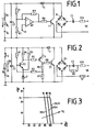
- the invention relates to a transformerless power supply with a first transistor, the main current path of which is connected via a rectifier device to an input AC voltage source and the control electrode of which is driven by the output voltage applied to a load and a capacitor connected in parallel therewith.
- a voltage stabilizer with a parallel transistor is known from Figure 19 on page 36 of the Valvo brochure "Properties and Applications of Silicon Zener Diodes", September 1968 edition.
- the base of the transistor lying parallel to the load is connected to the connection point of a resistor and a Zener diode, which are also parallel to the load.
- the input voltage which is, however, a DC voltage here, is supplied via a series resistor RV.
- this circuit has the short-circuit strength with a sufficiently large series resistor RV, but it is disadvantageous that the transistor takes over the entire charging current when idling and must therefore be designed for a relatively high power loss and also a constant power consumption in the amount of the nominal current occurs.
- the object of the invention is to design a transformerless power supply unit of the type mentioned at the outset in such a way that it is both short-circuit proof and has a low power loss when idling.
- control electrode of the first transistor is controlled by the output of a Schmitt trigger, the input voltage of which has an input and the other input of which is connected to a reference voltage, between the rectifier device and the input voltage source as a current source acting capacitive reactance is arranged and that there is a decoupling diode between the main current path of the first transistor and the load.
- This solution according to the invention has the advantage that it is short-circuit proof and consumes practically no active power when idling.
- the transformerless power supply unit according to the invention has a small volume and has a low outlay on components.
- the output voltage is well stabilized and is generally suitable for electrical devices with an output power of up to a few watts.
- the AC input voltage UE which for example represents a mains voltage of 220 volts, is fed to a bridge rectifier G1 via a series resistor R10 and a capacitor C1 representing the capacitive reactance.
- the output of the bridge rectifier G1 forming the plus potential is connected to the collector of a first transistor T1, which represents the switching transistor, and via a decoupling diode D to the one connection of a load RL and a smoothing capacitor C2 connected in parallel with it.
- the output of the bridge rectifier Gl forming the reference potential is connected to the emitter of the switching transistor T1 and to the other terminal of the load RL.
- a reference voltage Ur is applied to the inverting input (-) of the operational amplifier OP, the magnitude of which depends on the desired output voltage UA and the voltage divider ratio R1 / R2.
- the output of the operational amplifier is connected to the non-inverting input via a negative feedback resistor R11 and to the base of the transistor T1 via a resistor R8.
- the output of the Schmitt trigger switches transistor T1 conductive when the voltage at the non-inverting input which is proportional to the output voltage UA, exceeds its switch-on threshold.
- the current determined by the capacitive reactance C1 does not flow into the load RL but via the collector-emitter path of the transistor Tl past the load to the reference potential.
- the active power consumed during idle is low. Since in the event of a short circuit the current is practically a pure reactive current due to the lack of load resistance, the active power consumed is also low in this case.
- the ripple of the output voltage depends on the hysteresis of the Schmitt trigger.
- the switching frequency or the on or off duration of the Schmitt trigger and thus of the transistor T1 depends on the active power consumed by the load RL.
- FIG. 2 shows a detailed embodiment of the Schmitt trigger according to FIG. 1, which, despite its simplicity and the use of cheap components, is characterized by a good stabilization of the output voltage UA both with changing load current IA and with fluctuating input voltage UE .
- the Schmitt trigger shown here essentially consists of the two transistors T2 and T3, the collector of transistor T2 being connected to positive potential via resistor R4 and to the base of transistor T3 via resistor R5.
- the emitter of transistor T2, which forms the inverting input of the Schmitt trigger, is connected to positive potential via resistor R3 and to reference potential via Zener diode Z, which supplies the reference voltage here.
- the base of the transistor T2 represents the non-inverting input of the Schmitt trigger and is connected to the connection point of the voltage divider R1 / R2.
- the base point of the voltage divider Rl / R2 lies at the connection point of the collector resistor of the transistor T3, which is also designed as a voltage divider R6 / R7.
- the collector of transistor T3, whose emitter is connected to positive potential represents the output of the Schmitt trigger and is connected to the base of switching transistor T1 via resistor R8.
- the capacitor C1 forming the constant current source is bridged by a resistor R9 in order to discharge the capacitor Cl when the power plug is pulled.
- the series resistor R10 only serves to limit the current when the mains voltage UE is applied for the first moment. Since the power supply unit consumes practically no power when idling, the switch S can be connected in series to the load to switch the power supply unit on and off, so that it is not the mains voltage UE but only the lower output voltage UA that must be switched.
- the load can be a 24 volt motor, for example, which is part of a device that only requires a relatively low power (e.g. a few watts).
- FIG. 3 shows the output characteristic field as an example for an output voltage of 24 volts to be stabilized with a capacitor C1 of 1.5 / u F.
- the output voltage UA remains constant with a different load current IA up to a certain maximum load current, which is only dependent on the level of the input voltage UE.
- a Zener diode Z with a Zener voltage of 12 volts can be provided in FIG Transistor T2 drops. If the output voltage UA now rises to more than 24 volts, T2 becomes conductive, which pulls the base potential down from T3 to approximately plus 12 volts and thus T3 also becomes conductive. This also increases the base potential of the switching transistor T1 and this also switches through. If the output voltage now drops below 24 volts, the transistor T2 blocks, and with it the transistors T3 and T1, and current can flow back into the load circuit via the decoupling diode D.
- the blocking voltage of the switching transistor T1 is equal to the sum of the DC output voltage, superimposed AC voltage and forward voltage of the decoupling diode D.
- the blocking voltage of the rectifier bridge G1 is equal to the sum of the DC output voltage, superimposed AC voltage, forward voltage of the decoupling diode and twice the forward voltage of a rectifier diode.
Landscapes
- Engineering & Computer Science (AREA)
- Power Engineering (AREA)
- Dc-Dc Converters (AREA)
- Rectifiers (AREA)
- Discharge Heating (AREA)
- Coils Or Transformers For Communication (AREA)
- Details Of Television Scanning (AREA)
- Continuous-Control Power Sources That Use Transistors (AREA)
Abstract
Description
- Die Erfindung bezieht sich auf ein transformatorloses Netzgerät mit einem ersten Transistor, dessen Hauptstromstrecke über eine Gleichrichtereinrichtung mit einer Eingangswechselspannungsquelle in Verbindung steht und dessen Steuerelektrode von der an einer Last und einem dazu parallel geschalteten Kondensator anliegenden Ausgangsspannung angesteuert ist.
- Aus der Valvo Broschüre "Eigenschaften und Anwendungen von Silizium-Z-Dioden", Ausgabe September 1968, ist aus Bild 19 auf Seite 36 ein Spannungsstabilisator mit Paralleltransistor bekannt. Die Basis des parallel zur Last liegenden Transistors ist hierbei mit dem Verbindungspunkt eines Widerstandes und einer Zenerdiode, die ebenfalls parallel zur Last liegen, verbunden. Die Eingangsspannung, die allerdings hier eine Gleichspannung ist, wird über einen Vorwiderstand RV zugeführt. Wie auf Seite 39 der genannten Broschüre ausgeführt wird, ist bei dieser Schaltung die Kurzschlußfestigkeit bei genügend stark dimensioniertem Vorwiderstand RV zwar gegeben, nachteilig ist jedoch, daß bei Leerlauf der Transistor den gesamten Ladestrom übernimmt und daher für eine verhältnismäßig hohe Verlustleistung ausgelegt sein muß und außerdem ein ständiger Stromverbrauch in Höhe des Nennstromes auftritt.
- Aufgabe der Erfindung ist es, ein transformatorloses Netzteil der eingangs genannten Art so auszubilden, daß es sowohl kurzschlußfest ist als auch eine geringe Verlustleistung bei Leerlauf aufweist.
- Diese Aufgabe wird erfindungsgemäß dadurch gelöst, daß die Steuerelektrode des ersten Transistors vom Ausgang eines Schmitt-Triggers, dessen einer Eingang von der Ausgangsspannung beaufschlagt ist und dessen anderer Eingang an einer Referenzspannung liegt, angesteuert ist, daß zwischen der Gleichrichtereinrichtung und der Eingangsspannungsquelle ein als Stromquelle wirkender kapazitiver Blindwiderstand angeordnet ist und daß zwischen der Hauptstromstrecke des ersten Transistors und der Last eine Entkopplungsdiode liegt.
- Diese erfindungsgemäße Lösung weist den Vorteil auf, daß sie kurzschlußfest ist und im Leerlauf praktisch keine Wirkleistung verbraucht. Darüberhinaus hat das erfindungsgemäße transformatorlose Netzteil ein kleines Volumen und weist einen geringen Aufwand an Bauelementen auf. Es erfolgt eine gute Stabilisierung der Ausgangsspannung und eignet sich generell für elektrische Geräte mit bis zu einigen Watt Ausgangsleistung.
- Vorteilhafte Ausgestaltungen sind den Unteransprüchen entnehmbar.
- Im folgenden werden Ausführungsbeispiele der Erfindung an Hand der Zeichnung näher beschrieben.
- Es zeigen:
- Fig. 1 ein Blockschaltbild einer Ausführungsform,
- Fig. 2 eine detailliertere Darstellung der in Fig. 1 gezeigten Ausführungsform und
- Fig. 3 ein Ausgangskennlinienfeld als Beispiel bei einer bestimmten Dimensionierung.
- In dem in Fig. 1 dargestellten Blockschaltbild eines Ausführungsbeispiels der Erfindung wird die Eingangswechselspannung UE, die beispielsweise eine Netzspannung von 220 Volt darstellt, über einen Vorwiderstand R10 und einen den kapazitiven Blindwiderstand darstellenden Kondensator C1 einem Brückengleichrichter G1 zugeführt. Der das Pluspotential bildende Ausgang des Brückengleichrichters G1 liegt am Kollektor eines ersten Transistors T1, der den Schalttransistor darstellt, und über eine Entkopplungsdiode D an dem einen Anschluß einer Last RL und eines dazu parallel geschalteten Glättungskondentors C2. Der das Bezugspotential bildende Ausgang des Brückengleichrichters Gl liegt am Emitter des Schalttransistors T1 und am anderen Anschluß der Last RL. Parallel zur Last RL und dem Kondensator C2 liegt ein Spannungsteiler R1/R2, dessen oberer Anschlußpunkt mit der Kathode der zwischen diesem Anschlußpunkt und dem Kollektor des Transistors T1 liegenden Entkopplungsdiode D verbunden ist und dessen Verbindungspunkt an den nicht invertierenden Eingang (+) eines Operationsverstärkers OP geführt ist. An den invertierenden Eingang (-) des Operationsverstärkers OP ist eine Referenzspannung Ur gelegt, dessen Größe von der gewünschten Ausgangsspannung UA und dem Spannungsteilerverhältnis Rl/R2 abhängt. Der Ausgang des Operationsverstärkers ist über einen Gegenkopplungswiderstand R11 mit dem nicht invertierenden Eingang und über einen Widerstand R8 mit der Basis des Transistors T1 verbunden.
- Der Ausgang des Schmitt-Triggers schaltet den Transistor T1 leitend wenn die am nicht invertierenden Eingang liegende Spannung, die der Ausgangsspannung UA proportional ist, seine Einschaltschwelle überschreitet. Dadurch fließt der durch den kapazitiven Blindwiderstand C1 bestimmte Strom nicht in die Last RL sondern über die Kollektor-Emitter-Strecke des Transistors Tl an der Last vorbei zum Bezugspotential.
- Wenn die Ausgangsspannung UA soweit abgesunken ist, daß die am Eingang des Schmitt-Triggers anliegende Teilspannung die Ausschaltschwelle erreicht, wird der Schalttransistor Tl gesperrt und der Strom fließt über die Entkopplungsdiode D wieder in die Last RL bzw. den Kondensator C2.
- Da der Strom im Leerlauf im wesentlichen durch den Schalttransistor Tl an der Last RL vorbeifließt und dadurch fast ein reiner Blindstrom ist, ist die aufgenommene Wirkleistung im Leerlauf gering. Da bei Kurzschluß der Strom wegen Fehlens des Lastwiderstands ebenfalls praktisch ein reiner Blindstrom ist, ist auch in diesem Fall die aufgenommene Wirkleistung gering.
- Die Welligkeit der Ausgangsspannung hängt von der Hysterese des Schmitt-Triggers ab. Die Schaltfrequenz bzw. die Ein- oder Ausschaltdauer des Schmitt-Triggers und damit des Transsitors T1 hängt von der aufgenommenen Wirkleistung der Last RL ab.
- In Fig. 2 ist eine detaillierte Ausführungsform des Schmitt-Triggers nach Fig. 1 dargestellt, die sich, trotz ihrer Einfachheit und der Verwendung billiger Bauteile, durch eine gute Stabilisierung der Ausgangsspannung UA sowohl bei sich änderndem Laststrom IA als auch bei schwankender Eingangsspannung UE auszeichnet.
- Der hier dargestellte Schmitt-Trigger besteht im wesentlichen aus den beiden Transistoren T2 und T3, wobei der Kollektor des Transistors T2 über den Widerstand R4 mit Pluspotential und über den Widerstand R5 mit der Basis des Transistors T3 verbunden ist. Der den invertierenden Eingang des Schmitt-Triggers bildende Emitter des Transistors T2 ist über den Widerstand R3 mit Pluspotential und über die Zenerdiode Z, die hier die Referenzspannung liefert, mit Bezugspotential verbunden. Die Basis des Transistors T2 stellt den nicht invertierenden Eingang des Schmitt-Triggers dar und ist an den Verbindungspunkt des Spannungsteilers R1/R2 gelegt. Der Fußpunkt des Spannungsteilers Rl/R2 liegt am Verbindungspunkt des ebenfalls als Spannungsteiler R6/R7 ausgebildeten Kollektorwiderstandes des Transistors T3. Der Kollektor des Transistors T3, dessen Emitter an Pluspotential angeschlossen ist, stellt den Ausgang des Schmitt-Triggers dar und ist über den Widerstand R8 mit der Basis des Schalttransistors T1 verbunden.
- Der die Konstantstromquelle bildende Kondensator C1 ist mit einem Widerstand R9 überbrückt, um bei Ziehen des Netzsteckers den Kondensator Cl zu entladen. Der Vorwiderstand R10 dient lediglich dazu, den Strom bei Anlegen der Netzspannung UE im ersten Augenblick zu begrenzen. Da das Netzgerät im Leerlauf praktisch keine Leistung verbraucht, kann der Schalter S zum Ein- und Ausschalten des Netzgeräts in Serie zur Last geschaltet werden, so daß nicht die Netzspannung UE sondern lediglich die niedrigere Ausgangsspannung UA geschaltet werden muß.
- Die Last kann beispielsweise ein 24 Volt Motor sein, der Bestandteil eines Gerätes ist, das nur eine verhältnismäßig geringe Leistung (z.B. einige Watt) benötigt.
- In Fig. 3 ist als Beipiel für eine zu stabilisierende Ausgangsspannung von 24 Volt bei einem Kondensator C1 von 1,5 /u F das Ausgangskennlinienfeld dargestellt. Wie hieraus ersichtlich ist, bleibt die Ausgangsspannung UA bei unterschiedlichem Laststrom IA bis zu einem bestimmten maximalen Laststrom, der lediglich von der Höhe der Eingangsspannung UE abhängig ist, konstant. Z.B. bleibt die Ausgangsspannung UA konstant auf 24 Volt bis zu einem Ausgangsstrom von 76 mA bei UE = 195 Volt, von 88 mA bei UE = 220 Volt und von 96 mA bei UE = 245 Volt. Bei Kurzschluß oder Leerlauf des Netzgeräts fließt praktisch nur ein reiner Blindstrom, dessen Höhe durch die Kapazität von C1 bestimmt wird. Er entspricht den Werten in Fig. 3, in denen die dargestellten Kurven die Abszisse schneiden.
- Bei dem Beispiel einer Ausgangsspannung von UA = 24 Volt kann man in Fig. 2 eine Zenerdiode Z mit einer Zenerspannung von 12 Volt vorsehen, die Widerstände R1 und R2 gleich dimensionieren und den Widerstand R7 so, daß an ihm die Basis-Emitter-Spannung des Transistors T2 abfällt. Steigt nun die Ausgangsspannung UA auf über 24 Volt, wird T2 leitend, wodurch das Basispotential von T3 auf ca. plus 12 Volt heruntergezogen wird und somit T3 ebenfalls leitend wird. Hierdurch erhöht sich auch das Basispotential des Schalttransistors T1 und dieser schaltet ebenfalls durch. Sinkt nun die Ausgangsspannung auf unter 24 Volt, sperrt der Transistor T2 und damit auch die Transistoren T3 und T1 und es kann über die Entkopplungsdiode D wieder Strom in den Lastkreis fließen.
- Da also der Schalttransistor T1 entweder ganz gesperrt ist oder in der Sättigung betrieben wird und der von dem Kondensator C1 begrenzte Strom ein fast reiner Blindstrom ist, treten in dem Netzgerät nur sehr geringe Verlustleistungen auf.
- Es können auch billige Bauteile verwendet werden, da an den Transistoren und an den Dioden nur verhältnismäßig geringe Sperrspannungen auftreten. An den Transistoren T2 und T3 des Schmitt-Triggers und an der Entkopplungsdiode D sind die Sperrspannungen gleich der Summe der Ausgangsspannung und der überlagerten Wechselspannung. Die Sperrspannung des Schalttransistors T1 ist gleich der Summe von Ausgangsgleichspannung, überlagerter Wechselspannung und Durchlaßspannung der Entkopplungsdiode D. Die Sperrspannung der Gleichrichterbrücke G1 ist gleich der Summe von Ausgangsgleichspannung, überlagerter Wechselspannung, Durchlaßspannung der Entkopplungsdiode und zweimal der Durchlaßspannung einer Gleichrichterdiode.
Claims (7)
Priority Applications (1)
| Application Number | Priority Date | Filing Date | Title |
|---|---|---|---|
| AT86116808T ATE54781T1 (de) | 1985-12-20 | 1986-12-03 | Transformatorloses netzgeraet. |
Applications Claiming Priority (2)
| Application Number | Priority Date | Filing Date | Title |
|---|---|---|---|
| DE3545323 | 1985-12-20 | ||
| DE19853545323 DE3545323A1 (de) | 1985-12-20 | 1985-12-20 | Transformatorloses netzgeraet |
Publications (2)
| Publication Number | Publication Date |
|---|---|
| EP0229950A1 true EP0229950A1 (de) | 1987-07-29 |
| EP0229950B1 EP0229950B1 (de) | 1990-07-18 |
Family
ID=6289099
Family Applications (1)
| Application Number | Title | Priority Date | Filing Date |
|---|---|---|---|
| EP86116808A Expired - Lifetime EP0229950B1 (de) | 1985-12-20 | 1986-12-03 | Transformatorloses Netzgerät |
Country Status (3)
| Country | Link |
|---|---|
| EP (1) | EP0229950B1 (de) |
| AT (1) | ATE54781T1 (de) |
| DE (2) | DE3545323A1 (de) |
Cited By (5)
| Publication number | Priority date | Publication date | Assignee | Title |
|---|---|---|---|---|
| DE3727117A1 (de) * | 1987-08-14 | 1989-02-23 | Diehl Gmbh & Co | Verfahren zur erzeugung einer niedrigen stabilisierten gleichspannung |
| EP0324904A1 (de) * | 1988-01-20 | 1989-07-26 | Eaton GmbH | Netzteil zur Erzeugung einer geregelten Gleichspannung |
| EP0662748A3 (de) * | 1994-01-10 | 1995-10-11 | Motorola Inc | Spannungsregler und Verfahren dafür. |
| DE10002650A1 (de) * | 2000-01-21 | 2001-08-09 | Niels Dernedde | Schaltungsanordnung zur Reduktion der Wirkleistung in einer stabilisierten Gleichspannungsversorgung mittels eines Vorschaltkondensators |
| EP1276218A3 (de) * | 2001-07-12 | 2004-01-14 | Philips Intellectual Property & Standards GmbH | Elektrische Schaltungsanordnung |
Families Citing this family (4)
| Publication number | Priority date | Publication date | Assignee | Title |
|---|---|---|---|---|
| FR2706699B1 (fr) * | 1993-06-10 | 1995-09-15 | Gec Alsthom T & D Sa | Dispositif pour la fourniture d'une tension à un circuit électronique, en particulier à un circuit électronique associé à un capteur d'intensité placé sur une ligne électrique. |
| AT408155B (de) * | 1999-02-17 | 2001-09-25 | Egston Eggenburger Syst Elektr | Schaltungsanordnung zur erzeugung einer versorgungsspannung |
| DE102009033385B4 (de) | 2009-07-16 | 2018-09-20 | Diehl Ako Stiftung & Co. Kg | Netzteil-Schaltungsanordnung und Verfahren zum Betreiben einer Netzteil-Schaltungsanordnung |
| FR3083037A1 (fr) | 2018-06-25 | 2019-12-27 | Commissariat A L'energie Atomique Et Aux Energies Alternatives | Convertisseur abaisseur de tension |
Citations (3)
| Publication number | Priority date | Publication date | Assignee | Title |
|---|---|---|---|---|
| DE1513485A1 (de) * | 1965-07-08 | 1969-10-23 | Siemens Ag | Schaltung zur Erzeugung einer geregelten Gleichspannung |
| US3754182A (en) * | 1972-10-02 | 1973-08-21 | Litton Business Systems Inc | Switching voltage regulator with input low voltage and output voltage detectors |
| EP0106041B1 (de) * | 1982-09-23 | 1985-11-13 | Robert Bosch Gmbh | Stromversorgung |
Family Cites Families (2)
| Publication number | Priority date | Publication date | Assignee | Title |
|---|---|---|---|---|
| DE2809275A1 (de) * | 1978-03-03 | 1979-09-06 | Siemens Ag | Schaltungsanordnung zur erzeugung einer geregelten hohen gleichspannung aus einem drehstrom |
| US4347561A (en) * | 1980-12-17 | 1982-08-31 | Mclellan Norvel J | Alternating current to direct current power supply |
-
1985
- 1985-12-20 DE DE19853545323 patent/DE3545323A1/de not_active Withdrawn
-
1986
- 1986-12-03 DE DE8686116808T patent/DE3672794D1/de not_active Revoked
- 1986-12-03 AT AT86116808T patent/ATE54781T1/de not_active IP Right Cessation
- 1986-12-03 EP EP86116808A patent/EP0229950B1/de not_active Expired - Lifetime
Patent Citations (3)
| Publication number | Priority date | Publication date | Assignee | Title |
|---|---|---|---|---|
| DE1513485A1 (de) * | 1965-07-08 | 1969-10-23 | Siemens Ag | Schaltung zur Erzeugung einer geregelten Gleichspannung |
| US3754182A (en) * | 1972-10-02 | 1973-08-21 | Litton Business Systems Inc | Switching voltage regulator with input low voltage and output voltage detectors |
| EP0106041B1 (de) * | 1982-09-23 | 1985-11-13 | Robert Bosch Gmbh | Stromversorgung |
Cited By (7)
| Publication number | Priority date | Publication date | Assignee | Title |
|---|---|---|---|---|
| DE3727117A1 (de) * | 1987-08-14 | 1989-02-23 | Diehl Gmbh & Co | Verfahren zur erzeugung einer niedrigen stabilisierten gleichspannung |
| EP0324904A1 (de) * | 1988-01-20 | 1989-07-26 | Eaton GmbH | Netzteil zur Erzeugung einer geregelten Gleichspannung |
| EP0662748A3 (de) * | 1994-01-10 | 1995-10-11 | Motorola Inc | Spannungsregler und Verfahren dafür. |
| DE10002650A1 (de) * | 2000-01-21 | 2001-08-09 | Niels Dernedde | Schaltungsanordnung zur Reduktion der Wirkleistung in einer stabilisierten Gleichspannungsversorgung mittels eines Vorschaltkondensators |
| DE10002650C2 (de) * | 2000-01-21 | 2003-04-10 | Niels Dernedde | Schaltungsanordnung zur Reduktion der Wirkleistung in einer stabilisierten Gleichspannungsversorgung mittels eines Vorschaltkondensators |
| EP1276218A3 (de) * | 2001-07-12 | 2004-01-14 | Philips Intellectual Property & Standards GmbH | Elektrische Schaltungsanordnung |
| US6760233B2 (en) | 2001-07-12 | 2004-07-06 | Koninklijke Philips Electronics N.V. | Low-power low-voltage power supply |
Also Published As
| Publication number | Publication date |
|---|---|
| EP0229950B1 (de) | 1990-07-18 |
| DE3672794D1 (de) | 1990-08-23 |
| ATE54781T1 (de) | 1990-08-15 |
| DE3545323A1 (de) | 1987-06-25 |
Similar Documents
| Publication | Publication Date | Title |
|---|---|---|
| EP0421516B1 (de) | Stromversorgungseinrichtung mit Spannungsregelung und Strombegrenzung | |
| DE3204840A1 (de) | Gleichstromnetzgeraet mit stromkonstanthaltung, insbeondere fuer eine fernmeldeanlage | |
| EP0123085B1 (de) | Elektronisches Schaltnetzteil mit einem Drosselwandler | |
| EP0247409B1 (de) | Schaltnetzteil mit einem primär getakteten Gleichspannungswandler | |
| DE2809439A1 (de) | Schaltungseinrichtung zur steuerung des basisstromes eines als schalttransistor betriebenen leistungstransistors | |
| EP0229950B1 (de) | Transformatorloses Netzgerät | |
| DE2907673A1 (de) | Schaltungsanordnung zur ansteuerung eines bistabilen relais | |
| EP0057910B1 (de) | Schaltung zur geregelten Speisung eines Verbrauchers | |
| EP0030276B1 (de) | Schaltungsanordnung zum Laden einer Batterie | |
| EP0664602A1 (de) | Sperrumrichter mit geregelter Ausgangsspannung | |
| EP0106041B1 (de) | Stromversorgung | |
| DE4337461A1 (de) | Schaltnetzteil | |
| EP0081880A2 (de) | Regelungsschaltung zum Konstanthalten der Betriebsspannung eines elektrischen Verbrauchers | |
| DE3427520A1 (de) | Schaltungsanordnung zur speisung eines verbraucherzweipols | |
| EP1206830A1 (de) | Schaltnetzteil mit einrichtung zur begrenzung der ausgangsspannung | |
| DE2931042A1 (de) | Eintakt-durchflussumrichter zur erzeugung galvanisch getrennter ausgangsgleichspannungen | |
| EP0320605B1 (de) | Elektronisches Schaltnetzteil mit einem Drosselwandler | |
| EP0130411A2 (de) | Elektronisches Schaltnetzteil | |
| DE2830655C2 (de) | Elektronische Siebschaltung mit einem Transistorstellglied | |
| DE3232237C2 (de) | Elektronisches Schaltnetzteil | |
| DE2340286B1 (de) | Schaltung zur Betriebsspannungsversorgung der Zeilenendstufe in einem Fernsehempfaenger | |
| DE2260385C3 (de) | Gleichspannungsnetzgerät | |
| DE3420583A1 (de) | Sekundaer-schaltnetzteil | |
| DE2306818C3 (de) | Schaltungsanordnung zur Erzeugung einer einstellbaren geregelten Gleichspannung | |
| DE3241738A1 (de) | Schaltnetzgeraet |
Legal Events
| Date | Code | Title | Description |
|---|---|---|---|
| PUAI | Public reference made under article 153(3) epc to a published international application that has entered the european phase |
Free format text: ORIGINAL CODE: 0009012 |
|
| AK | Designated contracting states |
Kind code of ref document: A1 Designated state(s): AT CH DE FR GB IT LI NL |
|
| 17P | Request for examination filed |
Effective date: 19870812 |
|
| 17Q | First examination report despatched |
Effective date: 19890316 |
|
| ITF | It: translation for a ep patent filed | ||
| GRAA | (expected) grant |
Free format text: ORIGINAL CODE: 0009210 |
|
| AK | Designated contracting states |
Kind code of ref document: B1 Designated state(s): AT CH DE FR GB IT LI NL |
|
| REF | Corresponds to: |
Ref document number: 54781 Country of ref document: AT Date of ref document: 19900815 Kind code of ref document: T |
|
| GBT | Gb: translation of ep patent filed (gb section 77(6)(a)/1977) | ||
| ET | Fr: translation filed | ||
| REF | Corresponds to: |
Ref document number: 3672794 Country of ref document: DE Date of ref document: 19900823 |
|
| ITTA | It: last paid annual fee | ||
| PLBI | Opposition filed |
Free format text: ORIGINAL CODE: 0009260 |
|
| 26 | Opposition filed |
Opponent name: N.V. PHILIPS' GLOEILAMPENFABRIEKEN Effective date: 19910418 |
|
| NLR1 | Nl: opposition has been filed with the epo |
Opponent name: N.V. PHILIPS KGLOEILAMPENFABRIEKEN |
|
| PGFP | Annual fee paid to national office [announced via postgrant information from national office to epo] |
Ref country code: GB Payment date: 19911121 Year of fee payment: 6 |
|
| PGFP | Annual fee paid to national office [announced via postgrant information from national office to epo] |
Ref country code: FR Payment date: 19911127 Year of fee payment: 6 |
|
| PGFP | Annual fee paid to national office [announced via postgrant information from national office to epo] |
Ref country code: DE Payment date: 19911204 Year of fee payment: 6 |
|
| PGFP | Annual fee paid to national office [announced via postgrant information from national office to epo] |
Ref country code: AT Payment date: 19911205 Year of fee payment: 6 |
|
| PGFP | Annual fee paid to national office [announced via postgrant information from national office to epo] |
Ref country code: NL Payment date: 19911231 Year of fee payment: 6 |
|
| PGFP | Annual fee paid to national office [announced via postgrant information from national office to epo] |
Ref country code: CH Payment date: 19920212 Year of fee payment: 6 |
|
| RDAG | Patent revoked |
Free format text: ORIGINAL CODE: 0009271 |
|
| STAA | Information on the status of an ep patent application or granted ep patent |
Free format text: STATUS: PATENT REVOKED |
|
| REG | Reference to a national code |
Ref country code: CH Ref legal event code: PL |
|
| 27W | Patent revoked |
Effective date: 19920725 |
|
| GBPR | Gb: patent revoked under art. 102 of the ep convention designating the uk as contracting state | ||
| NLR2 | Nl: decision of opposition |