EP0232134A2 - Optische Platte und Plattengerät zum Aufzeichnen oder Wiedergeben von Daten in oder von der Platte - Google Patents
Optische Platte und Plattengerät zum Aufzeichnen oder Wiedergeben von Daten in oder von der Platte Download PDFInfo
- Publication number
- EP0232134A2 EP0232134A2 EP87300789A EP87300789A EP0232134A2 EP 0232134 A2 EP0232134 A2 EP 0232134A2 EP 87300789 A EP87300789 A EP 87300789A EP 87300789 A EP87300789 A EP 87300789A EP 0232134 A2 EP0232134 A2 EP 0232134A2
- Authority
- EP
- European Patent Office
- Prior art keywords
- data
- area
- optical disc
- sector
- read
- Prior art date
- Legal status (The legal status is an assumption and is not a legal conclusion. Google has not performed a legal analysis and makes no representation as to the accuracy of the status listed.)
- Granted
Links
Images





Classifications
-
- G—PHYSICS
- G11—INFORMATION STORAGE
- G11B—INFORMATION STORAGE BASED ON RELATIVE MOVEMENT BETWEEN RECORD CARRIER AND TRANSDUCER
- G11B7/00—Recording or reproducing by optical means, e.g. recording using a thermal beam of optical radiation by modifying optical properties or the physical structure, reproducing using an optical beam at lower power by sensing optical properties; Record carriers therefor
- G11B7/004—Recording, reproducing or erasing methods; Read, write or erase circuits therefor
-
- G—PHYSICS
- G11—INFORMATION STORAGE
- G11B—INFORMATION STORAGE BASED ON RELATIVE MOVEMENT BETWEEN RECORD CARRIER AND TRANSDUCER
- G11B7/00—Recording or reproducing by optical means, e.g. recording using a thermal beam of optical radiation by modifying optical properties or the physical structure, reproducing using an optical beam at lower power by sensing optical properties; Record carriers therefor
-
- G—PHYSICS
- G11—INFORMATION STORAGE
- G11B—INFORMATION STORAGE BASED ON RELATIVE MOVEMENT BETWEEN RECORD CARRIER AND TRANSDUCER
- G11B11/00—Recording on or reproducing from the same record carrier wherein for these two operations the methods are covered by different main groups of groups G11B3/00 - G11B7/00 or by different subgroups of group G11B9/00; Record carriers therefor
- G11B11/10—Recording on or reproducing from the same record carrier wherein for these two operations the methods are covered by different main groups of groups G11B3/00 - G11B7/00 or by different subgroups of group G11B9/00; Record carriers therefor using recording by magnetic means or other means for magnetisation or demagnetisation of a record carrier, e.g. light induced spin magnetisation; Demagnetisation by thermal or stress means in the presence or not of an orienting magnetic field
- G11B11/105—Recording on or reproducing from the same record carrier wherein for these two operations the methods are covered by different main groups of groups G11B3/00 - G11B7/00 or by different subgroups of group G11B9/00; Record carriers therefor using recording by magnetic means or other means for magnetisation or demagnetisation of a record carrier, e.g. light induced spin magnetisation; Demagnetisation by thermal or stress means in the presence or not of an orienting magnetic field using a beam of light or a magnetic field for recording by change of magnetisation and a beam of light for reproducing, i.e. magneto-optical, e.g. light-induced thermomagnetic recording, spin magnetisation recording, Kerr or Faraday effect reproducing
- G11B11/10595—Control of operating function
- G11B11/10597—Adaptations for transducing various formats on the same or different carriers
-
- G—PHYSICS
- G11—INFORMATION STORAGE
- G11B—INFORMATION STORAGE BASED ON RELATIVE MOVEMENT BETWEEN RECORD CARRIER AND TRANSDUCER
- G11B13/00—Recording simultaneously or selectively by methods covered by different main groups among G11B3/00, G11B5/00, G11B7/00 and G11B9/00; Record carriers therefor not otherwise provided for; Reproducing therefrom not otherwise provided for
- G11B13/04—Recording simultaneously or selectively by methods covered by different main groups among G11B3/00, G11B5/00, G11B7/00 and G11B9/00; Record carriers therefor not otherwise provided for; Reproducing therefrom not otherwise provided for magnetically or by magnetisation and optically or by radiation, for changing or sensing optical properties
-
- G—PHYSICS
- G11—INFORMATION STORAGE
- G11B—INFORMATION STORAGE BASED ON RELATIVE MOVEMENT BETWEEN RECORD CARRIER AND TRANSDUCER
- G11B19/00—Driving, starting, stopping record carriers not specifically of filamentary or web form, or of supports therefor; Control thereof; Control of operating function ; Driving both disc and head
- G11B19/02—Control of operating function, e.g. switching from recording to reproducing
- G11B19/04—Arrangements for preventing, inhibiting, or warning against double recording on the same blank or against other recording or reproducing malfunctions
-
- G—PHYSICS
- G11—INFORMATION STORAGE
- G11B—INFORMATION STORAGE BASED ON RELATIVE MOVEMENT BETWEEN RECORD CARRIER AND TRANSDUCER
- G11B20/00—Signal processing not specific to the method of recording or reproducing; Circuits therefor
- G11B20/10—Digital recording or reproducing
- G11B20/12—Formatting, e.g. arrangement of data block or words on the record carriers
- G11B20/1217—Formatting, e.g. arrangement of data block or words on the record carriers on discs
- G11B20/1252—Formatting, e.g. arrangement of data block or words on the record carriers on discs for discontinuous data, e.g. digital information signals or computer program data
-
- G—PHYSICS
- G11—INFORMATION STORAGE
- G11B—INFORMATION STORAGE BASED ON RELATIVE MOVEMENT BETWEEN RECORD CARRIER AND TRANSDUCER
- G11B27/00—Editing; Indexing; Addressing; Timing or synchronising; Monitoring; Measuring tape travel
- G11B27/10—Indexing; Addressing; Timing or synchronising; Measuring tape travel
- G11B27/102—Programmed access in sequence to addressed parts of tracks of operating record carriers
- G11B27/105—Programmed access in sequence to addressed parts of tracks of operating record carriers of operating discs
-
- G—PHYSICS
- G11—INFORMATION STORAGE
- G11B—INFORMATION STORAGE BASED ON RELATIVE MOVEMENT BETWEEN RECORD CARRIER AND TRANSDUCER
- G11B27/00—Editing; Indexing; Addressing; Timing or synchronising; Monitoring; Measuring tape travel
- G11B27/10—Indexing; Addressing; Timing or synchronising; Measuring tape travel
- G11B27/19—Indexing; Addressing; Timing or synchronising; Measuring tape travel by using information detectable on the record carrier
- G11B27/28—Indexing; Addressing; Timing or synchronising; Measuring tape travel by using information detectable on the record carrier by using information signals recorded by the same method as the main recording
- G11B27/30—Indexing; Addressing; Timing or synchronising; Measuring tape travel by using information detectable on the record carrier by using information signals recorded by the same method as the main recording on the same track as the main recording
- G11B27/3027—Indexing; Addressing; Timing or synchronising; Measuring tape travel by using information detectable on the record carrier by using information signals recorded by the same method as the main recording on the same track as the main recording used signal is digitally coded
-
- G—PHYSICS
- G11—INFORMATION STORAGE
- G11B—INFORMATION STORAGE BASED ON RELATIVE MOVEMENT BETWEEN RECORD CARRIER AND TRANSDUCER
- G11B7/00—Recording or reproducing by optical means, e.g. recording using a thermal beam of optical radiation by modifying optical properties or the physical structure, reproducing using an optical beam at lower power by sensing optical properties; Record carriers therefor
- G11B7/004—Recording, reproducing or erasing methods; Read, write or erase circuits therefor
- G11B7/0045—Recording
-
- G—PHYSICS
- G11—INFORMATION STORAGE
- G11B—INFORMATION STORAGE BASED ON RELATIVE MOVEMENT BETWEEN RECORD CARRIER AND TRANSDUCER
- G11B7/00—Recording or reproducing by optical means, e.g. recording using a thermal beam of optical radiation by modifying optical properties or the physical structure, reproducing using an optical beam at lower power by sensing optical properties; Record carriers therefor
- G11B7/007—Arrangement of the information on the record carrier, e.g. form of tracks, actual track shape, e.g. wobbled, or cross-section, e.g. v-shaped; Sequential information structures, e.g. sectoring or header formats within a track
- G11B7/00745—Sectoring or header formats within a track
-
- G—PHYSICS
- G11—INFORMATION STORAGE
- G11B—INFORMATION STORAGE BASED ON RELATIVE MOVEMENT BETWEEN RECORD CARRIER AND TRANSDUCER
- G11B7/00—Recording or reproducing by optical means, e.g. recording using a thermal beam of optical radiation by modifying optical properties or the physical structure, reproducing using an optical beam at lower power by sensing optical properties; Record carriers therefor
- G11B7/08—Disposition or mounting of heads or light sources relatively to record carriers
- G11B7/085—Disposition or mounting of heads or light sources relatively to record carriers with provision for moving the light beam into, or out of, its operative position or across tracks, otherwise than during the transducing operation, e.g. for adjustment or preliminary positioning or track change or selection
-
- G—PHYSICS
- G11—INFORMATION STORAGE
- G11B—INFORMATION STORAGE BASED ON RELATIVE MOVEMENT BETWEEN RECORD CARRIER AND TRANSDUCER
- G11B7/00—Recording or reproducing by optical means, e.g. recording using a thermal beam of optical radiation by modifying optical properties or the physical structure, reproducing using an optical beam at lower power by sensing optical properties; Record carriers therefor
- G11B7/08—Disposition or mounting of heads or light sources relatively to record carriers
- G11B7/09—Disposition or mounting of heads or light sources relatively to record carriers with provision for moving the light beam or focus plane for the purpose of maintaining alignment of the light beam relative to the record carrier during transducing operation, e.g. to compensate for surface irregularities of the latter or for track following
- G11B7/0941—Methods and circuits for servo gain or phase compensation during operation
-
- G—PHYSICS
- G11—INFORMATION STORAGE
- G11B—INFORMATION STORAGE BASED ON RELATIVE MOVEMENT BETWEEN RECORD CARRIER AND TRANSDUCER
- G11B7/00—Recording or reproducing by optical means, e.g. recording using a thermal beam of optical radiation by modifying optical properties or the physical structure, reproducing using an optical beam at lower power by sensing optical properties; Record carriers therefor
- G11B7/24—Record carriers characterised by shape, structure or physical properties, or by the selection of the material
- G11B7/2407—Tracks or pits; Shape, structure or physical properties thereof
- G11B7/24085—Pits
-
- G—PHYSICS
- G11—INFORMATION STORAGE
- G11B—INFORMATION STORAGE BASED ON RELATIVE MOVEMENT BETWEEN RECORD CARRIER AND TRANSDUCER
- G11B20/00—Signal processing not specific to the method of recording or reproducing; Circuits therefor
- G11B20/10—Digital recording or reproducing
- G11B20/12—Formatting, e.g. arrangement of data block or words on the record carriers
- G11B20/1217—Formatting, e.g. arrangement of data block or words on the record carriers on discs
- G11B2020/1259—Formatting, e.g. arrangement of data block or words on the record carriers on discs with ROM/RAM areas
-
- G—PHYSICS
- G11—INFORMATION STORAGE
- G11B—INFORMATION STORAGE BASED ON RELATIVE MOVEMENT BETWEEN RECORD CARRIER AND TRANSDUCER
- G11B2220/00—Record carriers by type
- G11B2220/20—Disc-shaped record carriers
- G11B2220/21—Disc-shaped record carriers characterised in that the disc is of read-only, rewritable, or recordable type
- G11B2220/211—Discs having both read-only and rewritable or recordable areas containing application data; Partial ROM media
-
- G—PHYSICS
- G11—INFORMATION STORAGE
- G11B—INFORMATION STORAGE BASED ON RELATIVE MOVEMENT BETWEEN RECORD CARRIER AND TRANSDUCER
- G11B2220/00—Record carriers by type
- G11B2220/20—Disc-shaped record carriers
- G11B2220/25—Disc-shaped record carriers characterised in that the disc is based on a specific recording technology
- G11B2220/2525—Magneto-optical [MO] discs
-
- G—PHYSICS
- G11—INFORMATION STORAGE
- G11B—INFORMATION STORAGE BASED ON RELATIVE MOVEMENT BETWEEN RECORD CARRIER AND TRANSDUCER
- G11B2220/00—Record carriers by type
- G11B2220/20—Disc-shaped record carriers
- G11B2220/25—Disc-shaped record carriers characterised in that the disc is based on a specific recording technology
- G11B2220/2537—Optical discs
Definitions
- the present invention relates to an optical disc on and from which data is recorded and reproduced and to a disc drive apparatus for writing and reading data into and from such an optical disc and, in particular, to an optical disc in which data can be additionally written on a read only type optical disc and to a drive apparatus for writing and reading data into and from such an optical disc.
- an optical disc drive apparatus using a read-only type optical disc (hereinafter, referred to as an R/O disc) in which data is recorded on a disc-shaped plastic material in the forms of concave and convex pits of the submicron order and the data is reproduced by irradiating a laser beam having a diameter of about l ⁇ m.
- R/O disc read-only type optical disc
- the R/O disc is constituted in the following manner.
- the data modulated concave and convex pits of the submicron order are formed on a plastic resin made of polycarbonate or the like having a thickness of l.2 mm.
- a reflecting layer made of aluminum or the like is evaporation deposited on the surface of the plastic resin and thereafter, a protecting layer is coated on the reflecting layer.
- the R/O disc has a diameter of l2 cm and a memory capacity of hundreds of mega bytes, additional data cannot be recorded.
- the R/O disc can be used as a disc in which the dictionary or font patterns for use in data base or word processors are stored, or as a disc in which programs or operating manual of computers are stored.
- the foregoing R/O disc is of the read-only type and is manufactured in a particular factory. Therefore, it is impossible for the user to use the disc by adding his preferred extra data to the dictionary or font patterns of the data base or word processor which were supplied in the R/O disc. In addition, patch cannot be added in order to correct bug in the program. Therefore, the R/O disc has a problem such that its application field in computers is limited.
- an object of the present invention to provide an optical disc in which the user can record additional data to the R/O disc and from which the user can well reproduce the data in the read-only area and those in the data recording area and further to provide a drive apparatus for writing and reading data into and from such an optical disc.
- an optical disc is constituted in the following manner. Namely, a recording material is formed in all of the tracks. A plurality of sectors are formed in the tracks. A sector has a sector identifier of the sector in which an address information is recorded and a data field portion to record data. A data field identification flag indicative of an read-only area or a data recording/reproducing area is recorded in the respective sector identifier. In this optical disc, the data field identification flag is detected. The kind of the area of a current sector is discriminated on the basis of the detected data field identification flag. Thus, the erroneous recording of data into the read-only area can be prevented. The waveform equalization and binary-clipping level of the reproduced data signal can be controlled upon reproduction of the data. The gain of the servo loop can be switched. The track searching operation can be stably performed.
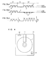
- Fig. l shows an external view of an embodiment of an optical disc of the present invention.
- Fig. l(a) is a plan view of the optical disc and
- Fig. l(b) is a cross sectional view taken along the line A-A′ in Fig. l(a).
- Fig. l shows an external view of an embodiment of an optical disc of the present invention.
- Fig. l(a) is a plan view of the optical disc
- Fig. l(b) is a cross sectional view taken along the line A-A′ in Fig. l(a).
- reference numeral l denotes an optical disc
- 2 is a center hole adapted to attach the optical disc to a disc motor
- 3 indicates data recording area of a plurality of tracks consisting of sectors having data field portions DF in which no data is recorded
- 4 data read-only area of a plurality of tracks consisting of sectors having data field portions DF in which data has previously been recorded
- 5 a disc substrate made of polycarbonate resin or the like
- 6 tracks which are formed as grooves in the disc substrate
- 7 a recording material in which signals can be optically or thermally recorded by a laser beam
- 8 a protecting layer to protect the recording material 7.
- S0, S1, S2, ..., S n denote sectors; ID represents sector identifier portions in which the address information of the sectors S0 to S n is recorded; and DF indicates the data field portions to record data.
- the optical disc l is constituted in the following manner.
- the groove-shaped tracks 6 are formed in the disc substrate 5.
- Each track is divided into a plurality of sectors comprising the sector identifier portions ID and data field portions DF.
- the recording material 7 is uniformly evaporation deposited on the disc substrate 5 having the tracks 6 so as to cover the whole surface of the disc.
- the beam signal can be recorded in the data recording area as changes in reflectance or a formation of holes. If the recording material 7 is a magnetooptic material, by reversals of the magnetic domain, the recorded signal can be read out on the basis of the rotation of the polarizing wave front of the reflected light by the Faraday effect. In the data read-only area 4, the recording material 7 functions as a reflecting film to reflect a reading laser beam of a weak power.
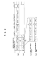
- Fig. 2 is an explanatory diagram of data field identification flags F (F1, F2) in the sector identifier portions ID of the optical disc in the foregoing embodiment.
- Fig. 2(a) shows a sector format of the data read-only area 4 in which data is recorded as concave and convex forms in the data field portion DF.
- Fig. 2(b) is a sector format of the data recording area 3 in which the data field portion DF is the groove-shaped track segment of a uniform depth.
- Fig. 2(c) shows a practical example of an address ADR, a data field identification flag F1, and error detection code CRC in the data read-only area 4.
- Fig. 2(d) shows a practical example of an address ADR, a data field identification flag F2, and error detection code CRC in the data recording area 3.
- PR denotes a preamble to reproduce a clock
- AM is an address mark to indicate the start of the address information
- ADR is the address
- F2 the data field identification flag indicative of the data recording area 3
- F1 the data field identification flag indicative of the data read-only area 4
- CRC the error detection code such as cyclic-redundancy code or the like
- PO a postamble.
- G1 and G2 denote gaps in which no information is recorded in order to absorb the fluctuation in the rotation of the optical disc.
- SYNC denotes a clock sync signal to reproduce a clock
- DM is a data mark indicative of the start of the data
- DATA indicates data
- ECC represents error detection/correction code
- RESYNC represents a RE-SYNC pattern to make word synchronization for data demodulation.
- the address ADR comprises: two bytes of the track address information; a track address (high byte) TA (H); a track address (low byte) TA (L); and sector address information SA.
- the optical disc drive apparatus immediately knows whether this sector belongs to that with the data read-only area 4 or that with the data recording area 3 and performs controls such as prevention of the erroneous writing of the data, waveform equalization of the reproduction signal, optimization of the servo loop gain, and stabilization of the search of a desired track, which will be explained hereinafter.
- Fig. 3 is an enlarged cross sectional view of the tracks of the optical disc in the foregoing embodiment.
- Fig. 3(a) illustrates a partial enlarged diagram of the sector identifier portion ID, gap G1, and data field portion DF in the data read-only area 4.
- Fig. 3(b) shows a partial enlarged diagram of the sector identifier portion ID, gap G1, and data field portion DF in the data recording area.
- Fig. 3(c) is a waveform diagram of the reproduction signal in the data recording area of Fig. 3(b).
- the tracks in the data read-only area 4 and data recording area 3 are formed with the same recording material 7.
- the address information of the sector is formed in each sector identifier portion ID by concave and convex pits P.
- the data is formed in the data field portion DF in the data read-only area 4 by concave and convex pits P similarly to the sector identifier portion ID.
- the data field portions DF in the data recording area 3 are grooves of a uniform depth, wherein data recorded by the user is recorded in the recording material 7 as dots D such as of reflectance changes, reversals of the magnetic domain, holes, or the like.
- the reproduction amplitude A1 of the pit portion P differs from the reproduction amplitude A2 of the dot portion D.
- the phase change recording material is evaporation deposited such that the depth of groove is equal to l/8 of the wavelength
- the following relation of the reflectances is satisfied: namely, the reflectance of the dot portion > the reflectance of the land portion > the reflectance of the pit portion.
- the frequency characteristics of the reproduction signals may also differ. Therefore, the waveform equalization amounts and the binary-clipping levels need to be controlled in accordance with the data recording area 3 and data readonly area 4.
- Fig. 4 is an external view of an embodiment of a cartridge of the optical disc of the invention.
- reference numeral l0 denotes a cartridge
- ll is a shutter of a window for recording and reproducing in order to irradiate a laser beam onto the optical disc l
- l2 is a disc identifier to identify the kind of disc such as R/O (read only) type, W/O (write once) type, W/E (erasable) type, or the like
- l3 a write protecting notch to set the permission/inhibition of the writing of the data into the data recording area 3 of the optical disc l.
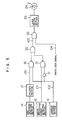
- Fig. 5 shows a block diagram of an embodiment of a write protecting circuit to permit/inhibit the writing of the data into the optical disc in the optical disc drive apparatus of the invention.
- Reference numeral l4 denotes a disc identifier detecting section to detect the disc identifier l2 of the cartridge; 15 is a write protecting notch detecting section to detect the setting of the write protecting notch l3 and to output a write protection detection signal l0l; l6 an address reading section to read the address information from the sector identifier ID of a current sector and to output a data field identification flag signal l02; l7 a decoder section for decoding the output of the disc identifier detecting section l4 and for generating an R/O disc detection signal l00; l8 and l9 two-input NAND gates; 2l an inverter; 20 and 22 AND gates; 23 a laser driving section; and 24 a semiconductor laser.
- the disc identifier detecting section l4 reads the disc identifier l2 of the cartridge l0 and interprets by the decoding section l7 and outputs the R/O disc detection signal l00.
- the notch dtecting section l5 reads the setting of the write protecting notch l3 of the cartridge l0 and outputs the write protection detection signal l0l.
- the address reading section l6 reads the sector identifier portion ID of the optical disc l by the laser beam and outputs the data field identification flag F of the sector identifier portion ID as the data field identification flag signal l02.
- the output of the NAND gate l8 becomes a low level by the signals l00 and l02, thereby setting a write protection signal l03 as the output of the AND gate 20 to be valid (low level). Since the signal l03 is at a low level, a write data signal l04 as an input to the laser driving circuit 23 is made invalid by the AND gate 22, so that the semiconductor laser 24 does not produce the recording power output.
- the output of the NAND gate l9 is set to a low level by the write protection detection signal l0l and by the signal of which the flag signal l02 was inverted by the inverter 2l if the signal l0l indicates the inhibition of the writing, thereby setting the write protection signal l03 as the output of the AND gate 20 to be valid (low level).
- the semiconductor laser 24 produces the recording power output as in the case of the foregoing data read-only area 4.
- the output of the NAND gate l9 becomes a high level, thereby making the signal l03 as the output of the AND gate 20 invalid (high level).
- the write data signal l04 is transmitted through the AND gate 22 and drives the laser driving section 23.
- the power of the semiconductor laser 24 is modulated by the recording power output, thereby recording the write data signal l04 into the current relevant sector.
- the erroneous writing of data into the data read-only area can be inhibited and at the same time, the permission/inhibition of the writing of data into the data recording area can be selectively and freely set.
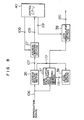
- Fig. 6 shows a block diagram of another embodiment of a write protecting circuit for permitting/inhibiting the writing of data into the optical disc drive apparatus in an information recording and reproducing apparatus of the present invention.
- Reference numeral 25 denotes a write protecting notch detecting section for detecting the setting of the write protecting notch l3 and for outputting a write protection detection signal l05;
- 26 is an address reading section for reading address information l07 and a data field identification flag signal ll0 which are included in the sector identifier portion ID of the sector from a reproduction signal l06;
- 27 an address comparing section for comparing the address information l07 with target address information l08;
- 28 a flag comparing section for comparing the flag signal ll0 with an input flag lll generated from CPU mentioned later;
- 29 a data modulating section for modulating input data ll5;
- 30 a laser driving circuit section; 3l a semiconductor laser; 32 an inverter; and 33 and 34 AND gates.
- the write protecting notch detecting section 25 reads the setting of the write protecting notch l3 of the cartridge l0 and outputs the write protection detection signal l05. Further, address reading section 26 reads the sector identifier portion ID of the optical disc l by a laser beam and outputs the address information l07 of the sector identifier portion ID to the address comparing section 27 and the data field identification flag signal ll0 to the flag comparing section 28.
- the section 27 compares the address information l07 with the target address information l08 and transmits an address coincidence output l09 to the AND gate 33.
- the flag comparing section 28 compares the input flag lll with the flag signal ll0 and outputs a flag coincidence output ll2 to the AND gate 34.
- the input flag lll is set by the CPU to correspond to the data field identification flag indicative of the data recording area 3.
- the flag signal ll0 differs from the input flag lll, so that the flag coincidence output ll2 of the flag comparing section 28 becomes invalid (low level). Therefore, even if the target address information l08 and a write command ll3 are applied in which the sector in the area 4 is used as the target sector and the address comparing section 27 outputs the address coincidence output l09 and the data modulating section 29 is made operative, a write data signal ll6 from the section 29 is blocked by the AND gate 34, and the input to the laser driving section 30 is made invalid, thereby preventing that the semiconductor laser 3l produces the recording power output. Thus, it is prevented that the data is erroneously written into the data field portion DF of the sector in the data read-only area 4.
- the input flag lll is set by the CPU to correspond to the data field identification flag indicative of the data recording area 3 and the flag coincidence signal ll2 becomes valid (high level).
- a signal ll7 of which the detection signal l05 was inverted by the inverter 32 sets the output of the AND gate 34 to a low level, thereby preventing that the semiconductor laser 3l produces the recording power output similarly as in the case of the foregoing data read-only area 4. If the detection signal l05 indicates the permission of the writing (low level), the output of the inverter 32 becomes a high level. Therefore, predetermined target address information l08 and write command ll3 are applied.
- the AND gate 33 makes a signal ll4 valid (high level) and the data modulating section 29 is made operative, so that the input data ll5 is modulated by the section 29 and is transmitted as the write data signal ll6 through the AND gate 34 and drives the laser driving section 30.
- the power of the semiconductor laser 3l is modulated by the recording power output, thereby recording the write data signal ll6 into the related sector.
- the erroneous writing of the data into the data read-only area can be inhibited and the permission/inhibition of the writing of data into the data recording area can be freely and selectively set.
- Fig. 7 is a track allocation diagram of the optical disc of the invention.
- Fig. 7(a) shows an embodiment of a track allocation which are divided into data read-only areas 35a and 35b and a data recording area 36a on the basis of sectors.
- This allocation is constituted by: the data read-only area 35a constituted from the track portions of track 0 and sectors S0 to S n , track l and sectors S0 to S n -- up to the track 2 and sector S1; the data recording area 36a from the track 2 and sector S2 up to the track (i+l) and sector S0; and the data read-only area 35b from the track (i+l) and sector S1 up to the track n and sector S n .
- a dummy sector DS1 corresponding to the track 2 and sector S2 is provided in the boundary between the areas 35a and 36a and belongs to the data recording area 36a.
- a dummy sector DS2 corresponding to the track (i+l) and the sector S1 is provided in the boundary between the areas 36a and 35b and belongs to the data read-only area 35b.
- Fig. 7(b) shows an embodiment of a track allocation which are divided into data read-only areas 35c and 35d and a data recording area 36b on the basis of tracks.
- This allocation is constituted by: the data read-only area 35c from the track 0 and sector S0 up to the track (i-l) and sector S n ; the data recording area 36b from the track i and sector S0 up to the track (l-l) and sector S n ; and the data read-only area 35d from the track l and sector S0 up to the track n and sector S n .
- Two dummy sectors DS 36a and DS 36b corresponding to the track i and sectors S0 and S1 are provided in the boundary between the areas 35c and 36b and belong to the data recording area 36b.
- Two dummy sectors DS 35a and DS 35b corresponding to the track l and sectors S0 and S1 are provided in the boundary between the areas 36b and 35d and belong to the data read-only area 35d.
- Each of the dummy sectors DS1, DS 36a , and DS 36b which belong to the data recording areas 36a and 36b comprises: the sector identifier portion ID having the data field identification flag F indicative of the data recording area; and the data field portion DF in which no data is recorded.
- Each of the dummy sectors DS2, DS 35a , and DS 35b which belong to the data read-only areas 35b and 35d comprises: the sector identifier portion ID having the data field identification flag F indicative of the data read-only area; and the data field portion DF where no data is preliminarily recorded.
- the reproduction signal can be read out of each area under the optimum reading condition by use of the data field identification flags in the sector identifier portions ID of the head dummy sectors of the data read-only areas 35b and 35d or of the data recording areas 36a and 36b.
- Fig. 8 shows a block diagram of a data reading circuit for performing the data reproduction from the optical disc in the optical disc drive apparatus of the invention.
- reference numeral 37 denotes a data equalization and binary signal generating section for performing the waveform equalization to correct the deterioration of the frequency characteristic of the reproduction signal l06 and converting the analog signal into binary signal;
- 38 is a data demodulating section for digitally demodulating the output of the section 37; 39 a level control section for generating a level control signal ll8 to control the waveform equalization amount and binary-clipping level of the section 37 in response to the data field identification flag signal ll0;
- 26 the address reading section for reading the address information and data field identification flag from the sector identifier portion ID;
- 27 the address comparing section for detecting the coincidence between the target address signal l08 and read address signal l07 and for outputting the address coincidence signal l09;
- 40 a control CPU for producing the target address signal l08 to control the data de
- the address reading section 26 reproduces the sector identifier portion ID of the optical disc by a laser beam and reads out the address information and data field identification flag of the sector identifier portion ID and outputs the address signal l07 and data field identification flag signal ll0.
- the waveform equalization amount and binary-clipping level of the address reading section 26 are set to the level for the data read-only area 4.
- the data field identification flag signal ll0 is referred to set the waveform equalization amount and binary-clipping level in the section 37 so that the bit error rate of the read data signal l20 becomes a minimum value when the reproduction signal l06 is demodulated by the data demodulating section 38.
- the level control signal ll8 sets the binary-clipping level of l/2 of the amplitude A1 of the reproduction signal of the sector identifier portion ID in Fig.
- the level control signal ll8 sets the binary clipping level of l/2 of the amplitude A2 of the reproduction signal of the data field portion DF in Fig. 3(c) into the section 37.
- the control CPU 40 outputs the target address signal l08 to the address comparing section 27.
- the section 27 outputs the address coincidence signal l09.
- the control CPU 40 detects the address coincidence signal l09, it outputs the data demodulation enable signal ll9 to the data demodulating section 38, thereby starting the data demodulating operation.
- the section 38 digitally demodulates the binary signal supplied from the section 37 and outputs the read data signal l20.
- the control CPU 40 If the address coincidence signal l09 is not detected, the control CPU 40 outputs the target address signal l08 having the address value of (the target address value - l) to the section 27.
- the section 27 When the read address signal l07 coincides with the new target address signal l08, the section 27 outputs the address coincidence signal l09.
- the data field identification flag signal ll0 which was read out of the sector corresponding to the target address signal l08 having the address value of (the target address value - l) supplies the level control signal ll8 such as to allow section 37 to perform the optimum reading operation.
- control CPU 40 detects the address coincidence signal l09 and waits for only the period of time corresponding to one sector and then outputs the data demodulation enable signal ll9 to the data demodulating section 38, thereby starting the data demodulating operation of the target sector.
- the foregoing operations correspond to the cases of the dummy sectors DS1 and DS2 in Fig. 7(a).
- the address value of (the target address value - 2) may be given to the target address signal l08 by use of the allocation with two dummy sectors DS 36a and DS 36b or DS 35a and DS 35b shown in Fig. 7(b).
- the control CPU 40 waits for only the period of time corresponding to two sectors after the address coincidence signal l09 was detected. Then, the CPU 40 outputs the data demodulation enable signal ll9 to the section 38, thereby reading out the target sector.
- the target address signals l08 indicative of the address value of (the target address value - l) and the address value of (the target address value - 2) data can be recovered and reproduced even from data read-only area or recording area with two continuous defective sector identifiers. Therefore, the optimum binary-clipping level and waveform equalization amount can be set with the high reliability and the data reading reliability can be increased.
- the dummy sectors are provided for the head sectors of the data read-only area and the data recording area, and the data recovery operations can be executed with those dummy sectors against possible errors caused in sector identifier portions. Therefore, the data field identification flags of all the sectors in the current related area can be detected with a high reliability.
- the data reading conditions can be controlled so as to correct the differences of the reproduction signal amplitudes and of the frequency characteristics of the data field portions. In this manner, the data can be read out of the R/O disc having the data recordable area with the high reliability.
- Fig. 9 shows a block diagram of the optical detecting system and the servo system in the optical disc drive apparatus.
- Reference numeral l denotes the optical disc for recording and reproducing information;
- 4l is a semiconductor laser of a wavelength ⁇ ; 42 and 43 condenser lenses;
- 44 a polarizing beam splitter;
- 45 a l/4 wavelength plate;
- 46 a focusing lens;
- 47 a focusing lens actuator;
- 48 a mirror to separate the reflected light;
- the light emitted from the semiconductor laser 4l progresses as indicated by broken lines and passes through the focusing lens 46 and is focused onto the track of the disc, thereby performing the recording and reproducing operations.
- the reflected light then passes through the beam splitter 44 and condenser lens 43 as shown by solid lines and is separated by the mirror 48.
- the separated lights enter the focusing photodetector 49 and tracking photodetector 50, respectively.
- a focus error signal l2l and a tracking error signal l22 are outputted through the difference amplifiers 5l and 52, respectively.
- Drive signals l23 and l24 of the focusing lens actuator are outputted by the focus servo circuit 53 and tracking servo circuit 54 and the focusing lens 46 is driven to the optimum position such that the error signals l2l and l22 become zero. In this manner, the well-known focus control and tracking control are performed.
- Fig. l0 is a detailed diagram of the focus servo circuit section 53.
- the focus error signal l2l derived from the focus servo photodetector 49 passes through a gain switching section 55 and a phase compensating section 56 and is supplied to a driving circuit section 57.
- the drive signal l23 is outputted to drive the focusing lens 46 so that the focus error signal l2l becomes zero.
- the flag signal ll0 is sent to the gain switching section 55 in the focus servo circuit section 53, thereby switching the gain such that the loop gain of the focus servo becomes constant.
- the loop gain of the focus servo decreases since the reflectance is small, and the deterioration of the servo tracking performance can be compensated, and the loop gain can be always made constant.
- the stable tracking servo can be also performed by constituting the circuit similarly to the foregoing focus servo.
- the optimum recording and reproducing operations of the R/O disc having the data recordable area can be executed.
- Fig. ll shows a block diagram of the optical detecting system, servo system, and search system in the optical disc drive apparatus of the invention.
- the parts and components indicated at reference numerals 4l to 54 are the same as those shown in Fig. 9.
- Reference numeral 58 denotes a differential amplifier; 59 is a traversed track number counting circuit section; 60 a comparator section for comparing the target track with the output of the counting circuit section 59 in order to detect their coincidence; 6l a target track address register for storing the target track address value; 62 a linear motor driving circuit section; and 63 a linear motor to move an optical head surrounded by a broken line.
- a focus sum signal l25 of the differential amplifier 58 is input to the counting circuit section 59 together with the tracking error signal l22.
- the true number of tracks which are traversed by the laser beam is counted and this true track number is obtained by correcting a possible eccentricity of the optical disc l from the polarity of the tracking error signal l22 using the phase of the focus sum signal l25 as a reference signal.
- the rough search by the linear motor 63 is executed in a manner such that the value of the target track address register section 6l is compared with the output of the counting circuit section 59 by the comparing section 60 and when they coincide, the driving of the linear motor driving circuit section 62 is stopped.
- the tracking servo circuit 54 After completion of the rough search, the tracking servo circuit 54 is made operative, thereby tracing a predetermined track.
- the track is again searched.
- the difference between the searched track and the target track is called the search error and this error is caused by the possible erroneous counting of the number of traversed tracks. If the search error is smaller than a predetermined value, the focusing lens actuator 47 is driven by the tracking servo circuit 54 to skip the tracks, thereby performing the fine search to move to the target track while checking the track address by the signal l07. If the search error is large, the linear motor is again driven and the rough search is reexecuted.
- Fig. l2 is an external view of an embodiment of the optical disc of the invention.
- reference numerals 64a and 64b denote guard areas where no data is recorded.
- guard areas 64a and 64b since no data is recorded in the guard areas 64a and 64b, these areas are not used for the search start address nor for the search target address.
- the guard areas 64a and 64b provided in the data read-only area 4 and data recording area 3 are larger than the numbers of erroneously searched tracks, when the searching operation is shifted from the data read-only area 4 (or data recording area 3) to the data recording area 3 (or data read-only area 4), the target area portion, in this just-mentioned case, the track in the area 3 (or area 4) can be accessed to after completion of the rough search by the linear motor 63 even in the worst case. Therefore, the fine search can be executed in the same portion of the data recording area 3 (or data read-only area 4), so that the problem of instability in the tracking servo can be solved.
- the area to which a target track belongs can be certainly accessed by the first trial of the search, so that any desired track can be stably searched.
- any desired track of the R/O disc having the data recordable area can be stably searched.
- the optical disc in which the user can freely record data into the R/O disc, and the data read-only area and the data recording area can be stably searched and the data can be accurately read out and to provide a drive apparatus of such an optical disc.
- the practical effects of the invention are large.
Landscapes
- Engineering & Computer Science (AREA)
- General Engineering & Computer Science (AREA)
- Signal Processing (AREA)
- Optical Recording Or Reproduction (AREA)
- Signal Processing For Digital Recording And Reproducing (AREA)
Priority Applications (1)
| Application Number | Priority Date | Filing Date | Title |
|---|---|---|---|
| EP93200206A EP0542730B1 (de) | 1986-02-07 | 1987-01-29 | Optische Platte und Plattengerät zum Aufzeichnen oder Wiedergeben von Daten in oder von der Platte |
Applications Claiming Priority (14)
| Application Number | Priority Date | Filing Date | Title |
|---|---|---|---|
| JP26374/86 | 1986-02-07 | ||
| JP26376/86 | 1986-02-07 | ||
| JP61026376A JPS62184628A (ja) | 1986-02-07 | 1986-02-07 | 光デイスク駆動装置 |
| JP61026374A JPS62184630A (ja) | 1986-02-07 | 1986-02-07 | 光デイスク |
| JP61029256A JPS62188026A (ja) | 1986-02-13 | 1986-02-13 | 情報記録装置 |
| JP29256/86 | 1986-02-13 | ||
| JP38839/86 | 1986-02-24 | ||
| JP61038839A JPS62197929A (ja) | 1986-02-24 | 1986-02-24 | 光デイスク駆動装置 |
| JP61046533A JPH0736224B2 (ja) | 1986-03-04 | 1986-03-04 | 光デイスクおよびその駆動装置 |
| JP46533/86 | 1986-03-04 | ||
| JP61113934A JPS62270032A (ja) | 1986-05-19 | 1986-05-19 | 光デイスク駆動装置 |
| JP113934/86 | 1986-05-19 | ||
| JP128669/86 | 1986-06-03 | ||
| JP61128669A JPH0760524B2 (ja) | 1986-06-03 | 1986-06-03 | 光デイスクおよび光デイスク駆動装置 |
Related Child Applications (1)
| Application Number | Title | Priority Date | Filing Date |
|---|---|---|---|
| EP93200206.6 Division-Into | 1993-01-26 |
Publications (3)
| Publication Number | Publication Date |
|---|---|
| EP0232134A2 true EP0232134A2 (de) | 1987-08-12 |
| EP0232134A3 EP0232134A3 (en) | 1988-12-28 |
| EP0232134B1 EP0232134B1 (de) | 1994-08-24 |
Family
ID=27564094
Family Applications (2)
| Application Number | Title | Priority Date | Filing Date |
|---|---|---|---|
| EP93200206A Expired - Lifetime EP0542730B1 (de) | 1986-02-07 | 1987-01-29 | Optische Platte und Plattengerät zum Aufzeichnen oder Wiedergeben von Daten in oder von der Platte |
| EP87300789A Expired - Lifetime EP0232134B1 (de) | 1986-02-07 | 1987-01-29 | Optische Platte und Plattengerät zum Aufzeichnen oder Wiedergeben von Daten in oder von der Platte |
Family Applications Before (1)
| Application Number | Title | Priority Date | Filing Date |
|---|---|---|---|
| EP93200206A Expired - Lifetime EP0542730B1 (de) | 1986-02-07 | 1987-01-29 | Optische Platte und Plattengerät zum Aufzeichnen oder Wiedergeben von Daten in oder von der Platte |
Country Status (6)
| Country | Link |
|---|---|
| US (1) | US5023854A (de) |
| EP (2) | EP0542730B1 (de) |
| KR (2) | KR900009188B1 (de) |
| CN (1) | CN1004238B (de) |
| CA (1) | CA1277028C (de) |
| DE (2) | DE3752097T2 (de) |
Cited By (5)
| Publication number | Priority date | Publication date | Assignee | Title |
|---|---|---|---|---|
| DE3913992A1 (de) * | 1988-04-27 | 1989-11-09 | Toshiba Kawasaki Kk | Optisches plattengeraet |
| EP0618582A3 (de) * | 1993-03-31 | 1995-02-15 | Sony Corp | Informationsverarbeitungsgerät. |
| WO1998003973A3 (en) * | 1996-07-24 | 1998-03-19 | Philips Electronics Nv | Improvements in and relating to optically readable discs and disc recording apparatus |
| EP1308951A3 (de) * | 1998-06-15 | 2007-05-23 | Samsung Electronics Co., Ltd. | Aufzeichnungsmedium zur Speicherung von Schreibschutzinformationen und Schreibschutzverfahren dazu |
| EP1168314A3 (de) * | 1997-04-16 | 2008-10-01 | Matsushita Electric Industrial Co., Ltd. | Platte und Plattenaufzeichnungsgerät |
Families Citing this family (101)
| Publication number | Priority date | Publication date | Assignee | Title |
|---|---|---|---|---|
| DE3784318T2 (de) * | 1986-11-21 | 1993-06-09 | Olympus Optical Co | Verfahren und geraet zum aufzeichnen von signalen auf einen plattenfoermigen optischen aufzeichnungstraeger und plattenfoermiger optischer aufzeichnungstraeger. |
| DE3884354T2 (de) * | 1987-11-30 | 1994-01-20 | Toshiba Kawasaki Kk | Gerät zum Fokussieren eines Lichtstrahls auf einem Informationsspeichermedium. |
| EP0329122B1 (de) * | 1988-02-19 | 1993-08-11 | Philips and Du Pont Optical Company | Verfahren zur Befestigung von Informationen an einer optischen Scheibe, die ausschliesslich zum Lesen vorbereitet ist |
| FR2632747A2 (fr) * | 1988-03-24 | 1989-12-15 | Salzmann Jean Loup | Dispositif de protection des ordinateurs contre les programmes malveillants appeles virus |
| FR2629231A1 (fr) * | 1988-03-24 | 1989-09-29 | Salzmann Jean Loup | Dispositif de protection des ordinateurs contre les programmes malveillants appeles " virus " |
| EP0363195B1 (de) * | 1988-10-05 | 1995-08-02 | Pioneer Electronic Corporation | Plattenspieler mit Servokreis von variabler Übertragungsfunktion |
| US5214627A (en) * | 1989-02-08 | 1993-05-25 | Fujitsu Limited | Optical disk having read-exclusive and write-enable regions |
| JPH03130972A (ja) * | 1989-10-16 | 1991-06-04 | Matsushita Electric Ind Co Ltd | トラック検索装置及びトラッキング制御装置 |
| US5233576A (en) * | 1989-10-25 | 1993-08-03 | Hewlett-Packard Company | Multi-function optical disk drive and media |
| DE69026571T2 (de) * | 1989-10-25 | 1996-09-12 | Hewlett Packard Co | System mit einer multifunktionalen Platte und derselben Antrieb |
| JP2998161B2 (ja) * | 1990-01-17 | 2000-01-11 | 富士通株式会社 | 記録媒体の同期信号読取方法及び装置 |
| US5138598A (en) * | 1990-01-25 | 1992-08-11 | Sony Corporation | Optical disk having relatively wide ram tracks and relatively narrow rom tracks |
| JP3141242B2 (ja) * | 1990-08-24 | 2001-03-05 | ソニー株式会社 | 光ディスク記録装置 |
| US5265230A (en) * | 1990-08-29 | 1993-11-23 | Hewlett-Packard Company | Method and apparatus for determining sector status in a data storage device by writing a status of read-only, writable, or obliterated in an error recovery area of each sector |
| JP3315711B2 (ja) * | 1990-09-17 | 2002-08-19 | ヒューレット・パッカード・カンパニー | 磁気光学ディスクデータ記憶装置の書き込み管理システム及び方法 |
| US5132954A (en) * | 1990-09-24 | 1992-07-21 | International Business Machines Corporation | Controls for optical disk relating to accessing and utilization of such disk |
| JP2531847B2 (ja) * | 1990-09-27 | 1996-09-04 | インターナシヨナル・ビジネス・マシーンズ・コーポレーシヨン | 光学ディスク駆動装置 |
| JP2646825B2 (ja) * | 1990-10-01 | 1997-08-27 | 三菱電機株式会社 | 光ディスク装置 |
| JP2940208B2 (ja) * | 1991-04-12 | 1999-08-25 | 松下電器産業株式会社 | 記録再生方法、および記録再生装置、光ディスク |
| JP3158557B2 (ja) * | 1991-09-27 | 2001-04-23 | ソニー株式会社 | 再生装置 |
| US5642458A (en) * | 1992-11-18 | 1997-06-24 | Canon Kabushiki Kaisha | Video signal processing apparatus |
| JP2763080B2 (ja) * | 1992-03-18 | 1998-06-11 | 富士通株式会社 | 光ディスク装置 |
| US5680382A (en) * | 1992-04-10 | 1997-10-21 | Canon Kabushiki Kaisha | Optical information recording apparatus and method capable of handling a plurality of card-like recording media of different reflectance |
| US5592448A (en) * | 1992-05-08 | 1997-01-07 | Hitachi, Ltd. | Access control apparatus for optical disk according change of track pitch |
| JPH0628778A (ja) * | 1992-05-14 | 1994-02-04 | Matsushita Electric Ind Co Ltd | 光ディスクおよび光情報記録再生装置 |
| US5297115A (en) * | 1992-07-30 | 1994-03-22 | Maxoptix Corporation | Detection of saved sectors on an optical disk |
| JPH0668588A (ja) * | 1992-08-19 | 1994-03-11 | Olympus Optical Co Ltd | 可換媒体記録再生装置 |
| JPH0684174A (ja) * | 1992-09-03 | 1994-03-25 | Hitachi Ltd | 光ディスク媒体とそれを用いた情報処理装置 |
| JPH06111334A (ja) * | 1992-09-24 | 1994-04-22 | Sony Corp | 円盤状記録媒体用の記録及び/又は再生装置、光検出器及び光ヘッド |
| CN1039556C (zh) * | 1993-04-14 | 1998-08-19 | 三星电子株式会社 | 光迹计数伺服电路及其方法 |
| EP1045377A3 (de) * | 1993-06-08 | 2011-03-16 | Panasonic Corporation | Optische Platte sowie Vorrichtung zur Informationsaufnahme/wiedergabe |
| JP2982571B2 (ja) * | 1993-08-05 | 1999-11-22 | 日本ビクター株式会社 | デジタルデータ記録再生方法 |
| US5446716A (en) * | 1994-01-10 | 1995-08-29 | Eastman Kodak Company | Laser power control in an optical recording system to compensate for multiple system degradations |
| JP3318636B2 (ja) * | 1994-03-31 | 2002-08-26 | ソニー株式会社 | サーボ装置、光ディスク再生装置 |
| KR0129968B1 (ko) * | 1994-06-30 | 1998-04-18 | 김광호 | 광디스크장치에 있어서 횡단트랙 계수회로 |
| KR960706160A (ko) * | 1994-08-31 | 1996-11-08 | 이데이 노부유키 | 광디스크와 기록 및/또는 재생장치(Optical disk and recording and/or reproducing apparatus) |
| JP3707812B2 (ja) * | 1994-09-27 | 2005-10-19 | ソニー株式会社 | 光記録方法、光記録装置及び光記録媒体 |
| CN1127079C (zh) * | 1995-08-10 | 2003-11-05 | 索尼公司 | 数据传递方法、记录装置和再现装置 |
| JPH09251761A (ja) * | 1996-03-15 | 1997-09-22 | Pioneer Electron Corp | 情報記録媒体並びにその記録装置及び再生装置 |
| EP1006514B1 (de) | 1996-10-23 | 2003-01-02 | Matsushita Electric Industrial Co., Ltd. | Optische Platte |
| US5787068A (en) * | 1996-11-07 | 1998-07-28 | Imation Corp. | Method and arrangement for preventing unauthorized duplication of optical discs using barriers |
| KR19980084908A (ko) | 1997-05-27 | 1998-12-05 | 윤종용 | 비휘발성 메모리를 갖는 광 디스크와 비휘발성 메모리를 갖는 광 디스크를 사용하기 위한 광 디스크 장치 및 그 제어 방법 |
| US6035376A (en) * | 1997-10-21 | 2000-03-07 | Apple Computer, Inc. | System and method for changing the states of directory-based caches and memories from read/write to read-only |
| US6185661B1 (en) | 1998-01-02 | 2001-02-06 | Emc Corporation | Worm magnetic storage device |
| JPH11306647A (ja) * | 1998-04-24 | 1999-11-05 | Sony Corp | 記録再生装置および方法、提供媒体、並びに記録媒体 |
| US6744713B1 (en) * | 1998-06-15 | 2004-06-01 | Samsung Electronics Co., Ltd. | Recording medium for storing write protection information and write protection method thereof |
| JP3754834B2 (ja) * | 1998-11-09 | 2006-03-15 | パイオニア株式会社 | 記録再生装置 |
| US20030157292A1 (en) * | 1999-06-23 | 2003-08-21 | Dataplay, Inc. | Miniature optical disk for data storage |
| US6823398B1 (en) | 2000-03-31 | 2004-11-23 | Dphi Acquisitions, Inc. | File system management embedded in a storage device |
| US6990058B1 (en) | 2000-04-03 | 2006-01-24 | Dphi Acquisitions, Inc. | Structure and method for storing data on optical disks |
| JP2001291244A (ja) * | 2000-04-04 | 2001-10-19 | Sharp Corp | 光記録媒体、光記録情報の再生方法並びに再生装置 |
| US6598135B1 (en) * | 2000-05-03 | 2003-07-22 | Plasmon Ide | System and method for defining rewriteable data storage media as write once data storage media |
| US7051054B1 (en) | 2000-05-30 | 2006-05-23 | Dphi Acquisitions, Inc. | Method and apparatus for emulating read/write file system on a write-once storage disk |
| EP1436700A2 (de) * | 2000-05-30 | 2004-07-14 | DPHI Aquisitions, Inc. | Fehlerverwaltungssystem für einmal beschreibbare speicherplatte |
| US6738333B1 (en) | 2000-05-30 | 2004-05-18 | Dphi Acquisitions, Inc. | Format for recording data in a storage disk |
| US6970410B2 (en) * | 2001-01-25 | 2005-11-29 | Dphi Acquisitions, Inc. | Focus detection in a digital focus servo system |
| US6728182B2 (en) | 2001-01-25 | 2004-04-27 | Dphi Acquisitions, Inc. | Tracking and focus servo system with a media type boundary crossing detector |
| US7095683B2 (en) * | 2001-01-25 | 2006-08-22 | Dphi Acquisitions, Inc. | Tracking and focus digital servo system with write abort |
| US6809995B2 (en) | 2001-01-25 | 2004-10-26 | Dphi Acquisitions, Inc. | Digital focus and tracking servo system |
| US7023766B2 (en) | 2001-01-25 | 2006-04-04 | Dphi Acquisitions, Inc. | Flexible servicing of servo algorithms using a digital signal processor |
| US6738320B2 (en) | 2001-01-25 | 2004-05-18 | Dphi Acquisitions, Inc. | System and method for moving optical pick up from current position to target position with smooth control |
| US6909676B2 (en) * | 2001-01-25 | 2005-06-21 | Dphi Acquisitions, Inc. | Digital tracking servo system with multi-track seek with track zero crossing detection |
| US7522480B2 (en) | 2001-01-25 | 2009-04-21 | Dphi Acquisitions, Inc. | Digital tracking servo system with multi-track seek with an acceleration clamp |
| US6847597B2 (en) | 2001-01-25 | 2005-01-25 | Dphi Acquisitions, Inc. | Optical disk drive with a digital focus and tracking servo system |
| US7196979B2 (en) | 2001-01-25 | 2007-03-27 | Dphi Acquisitions, Inc. | Calibration storage methods for a digital focus and tracking servo system with calibration |
| US6937543B2 (en) | 2001-01-25 | 2005-08-30 | Dphi Acquisitions, Inc. | Digital focus servo system with a sliding notch filter |
| US6891781B2 (en) * | 2001-01-25 | 2005-05-10 | Dphi Acquisitions, Inc. | Digital servo system with second order compensator |
| US6813226B2 (en) | 2001-01-25 | 2004-11-02 | Dphi Acquisitions, Inc. | Calibration of a focus sum threshold in a focus servo system |
| US6813228B2 (en) | 2001-01-25 | 2004-11-02 | Dphi Acquisitions, Inc. | Tracking and focus servo system with direction sensor |
| US6906985B2 (en) | 2001-01-25 | 2005-06-14 | Dphi Acquisitions, Inc. | Calibration of tracking error signal gain in a tracking servo system |
| US6970403B2 (en) * | 2001-01-25 | 2005-11-29 | Dphi Acquisition, Inc. | Calibration of tracking error signal offset in a tracking servo system |
| US7680004B2 (en) * | 2001-01-25 | 2010-03-16 | Dphi Acquisitions, Inc. | Digital servo system with inverse non-linearity compensation |
| US7092322B2 (en) * | 2001-01-25 | 2006-08-15 | Dphi Acquisitions, Inc. | Calibration of focus error signal offset in a focus servo system |
| US6781929B2 (en) | 2001-01-25 | 2004-08-24 | Dphi Acquisitions, Inc. | Digital tracking servo system with multi-track seek |
| US7023776B2 (en) * | 2001-01-25 | 2006-04-04 | Dphi Acquisitions, Inc. | Calibration initiation methods for a tracking and focus servo system |
| US6930963B2 (en) | 2001-01-25 | 2005-08-16 | Dphi Acquistions, Inc. | Tracking and focus servo system with head load |
| US7492675B2 (en) * | 2001-01-25 | 2009-02-17 | Dphi Acquisitions, Inc. | Digital servo system with calibrated notch filters |
| US7020054B2 (en) * | 2001-01-25 | 2006-03-28 | Dphi Acquisitions, Inc. | Digital servo system with biased feed-forward |
| US6965547B2 (en) * | 2001-01-25 | 2005-11-15 | Dphi Acquisitions, Inc. | Tracking and focus servo system with error signal inverse non-linearity calibration |
| US6904007B2 (en) * | 2001-01-25 | 2005-06-07 | Dphi Acquisitions, Inc. | Digital servo system with loop gain calibration |
| US6704261B2 (en) | 2001-01-25 | 2004-03-09 | Dphi Acquisitions, Inc. | Spin motor control in an optical drive |
| US6956797B2 (en) * | 2001-01-25 | 2005-10-18 | Dphi Acquisitions, Inc. | Digital servo system with error signal integrity testing |
| US6898164B2 (en) | 2001-01-25 | 2005-05-24 | Dphi Acquisitions, Inc. | Close tracking algorithm in a digital tracking servo system |
| US6922380B2 (en) | 2001-01-25 | 2005-07-26 | Dphi Acquisitions, Inc. | Tracking and focus servo system with anti-skate algorithm |
| US6762980B2 (en) | 2001-01-25 | 2004-07-13 | Dphi Acquisitions, Inc. | Digital tracking servo system with a multi-track seeking and accelerated servo function for regaining a closed tracking loop |
| US6891789B2 (en) * | 2001-01-25 | 2005-05-10 | Dphi Acquisitions, Inc. | Tracking and focus servo system with automatic media type detector |
| US7016280B2 (en) * | 2001-01-25 | 2006-03-21 | Dphi Acquisitions, Inc. | Tracking and focus servo system with defect detection |
| US6882603B2 (en) * | 2001-01-25 | 2005-04-19 | Dphi Acquisitions, Inc. | Digital tracking servo system with tracking skate detection |
| US7782721B2 (en) * | 2001-01-25 | 2010-08-24 | Dphi Acquisitions, Inc. | Digital focus and tracking servo system with multi-zone calibration |
| US7414940B2 (en) | 2001-01-25 | 2008-08-19 | Dphi Acquisitions, Inc. | Calibration of a focus error signal gain in a focus servo system |
| US7672199B2 (en) | 2001-01-25 | 2010-03-02 | Dphi Acquisitions, Inc. | Close focus algorithm in a digital focus servo system |
| US6847596B2 (en) | 2001-01-25 | 2005-01-25 | Dphi Acquisitions, Inc. | Tracking servo system including a multi-track seek algorithm with a track zero crossing period integrity test |
| US7593300B2 (en) | 2001-01-25 | 2009-09-22 | Dphi Acquisitions, Inc. | Digital tracking servo system with off-format detection |
| US6885619B2 (en) | 2001-01-25 | 2005-04-26 | Dphi Acquisitions, Inc. | Detector input stray light offset calibration in an optical disk drive |
| US6950380B2 (en) * | 2001-01-25 | 2005-09-27 | Dphi Acquisitions, Inc. | Detector input dark current offset calibration in an optical disk drive digital servo |
| US7260031B2 (en) | 2001-01-25 | 2007-08-21 | Dphi Acquisitions, Inc. | Digital focus and tracking servo system with one-track jump |
| US6958957B2 (en) * | 2001-01-25 | 2005-10-25 | Dphi Acquisitions, Inc. | Digital tracking and focus servo system with TES to FES crosstalk calibration |
| US6882601B2 (en) | 2001-01-25 | 2005-04-19 | Dphi Acquisitions, Inc. | Digital servo system with feed-forward control loops |
| US7724613B2 (en) * | 2007-07-03 | 2010-05-25 | International Business Machines Corporation | Apparatus and method to store information in a holographic data storage medium |
| KR101496975B1 (ko) * | 2008-05-28 | 2015-03-02 | 삼성전자주식회사 | 고체 상태 디스크 및 이에 대한 입출력방법 |
| JP2014160523A (ja) * | 2013-02-20 | 2014-09-04 | Funai Electric Co Ltd | 光ディスク装置、及びイコライザ調整方法 |
Citations (2)
| Publication number | Priority date | Publication date | Assignee | Title |
|---|---|---|---|---|
| US4269917A (en) | 1979-07-06 | 1981-05-26 | Drexler Technology Corporation | Data storage medium having reflective particulate silver layer |
| US4484319A (en) | 1980-09-19 | 1984-11-20 | Matsushita Electric Industrial Co., Ltd. | Apparatus for locating a track on disc-like optical information carriers |
Family Cites Families (39)
| Publication number | Priority date | Publication date | Assignee | Title |
|---|---|---|---|---|
| US4229808A (en) * | 1978-12-21 | 1980-10-21 | Ncr Corporation | Method for recording multiple data segments on a storage disc with eccentricity factor |
| US4301486A (en) * | 1979-06-04 | 1981-11-17 | Texas Instruments, Inc. | System for recording information on a flexible information storage media |
| US4296491A (en) * | 1979-07-30 | 1981-10-20 | Atlantic Richfield Company | Information carrier having inter-track identification code information |
| US4467383A (en) * | 1980-02-23 | 1984-08-21 | Sharp Kabushiki Kaisha | Magnetooptic memory medium |
| JPS57130240A (en) * | 1981-02-05 | 1982-08-12 | Olympus Optical Co Ltd | Optical information recording and reproducing device and information recording medium for it |
| US4599718A (en) * | 1981-04-07 | 1986-07-08 | Tdk Electronics Co., Ltd. | Method for erasing a light recording medium |
| US4523304A (en) * | 1981-04-17 | 1985-06-11 | Matsushita Electric Industrial Co., Ltd. | Optical data recording and reproducing apparatus |
| US4385372A (en) * | 1981-05-01 | 1983-05-24 | Drexler Technology Corporation | Reflective optical data storage and laser recording media having grooved dielectric encoded prerecorded information |
| JPS589226A (ja) * | 1981-07-07 | 1983-01-19 | Toshiba Corp | 光ディスク装置 |
| US4417330A (en) * | 1981-10-15 | 1983-11-22 | Burroughs Corporation | Optical memory system providing improved focusing control |
| KR880000999B1 (ko) * | 1981-11-25 | 1988-06-10 | 미쓰다 가쓰시게 | 광학적 정보 기억장치 |
| US4546462A (en) * | 1981-12-04 | 1985-10-08 | Matsushita Electric Industrial Co., Ltd. | Optical data recording and reproducing apparatus |
| NL8200415A (nl) * | 1982-02-04 | 1983-09-01 | Philips Nv | Optische uitleesbare informatieschijf. |
| JPS58158038A (ja) * | 1982-03-15 | 1983-09-20 | Toshiba Corp | 光デイスク装置 |
| US4519056A (en) * | 1982-03-15 | 1985-05-21 | Tokyo Shibaura Denki Kabushiki Kaisha | Optical disk apparatus |
| JPS58181163A (ja) * | 1982-04-16 | 1983-10-22 | Hitachi Ltd | 記憶装置の制御方式 |
| DE3318497C2 (de) * | 1982-05-23 | 1994-03-10 | Sony Corp | Wiedergabeanordnung für die Wiedergabe digitaler Daten von einem Aufzeichnungsträger nach einem Suchlauf |
| EP0095766B1 (de) * | 1982-05-31 | 1986-10-22 | Hitachi, Ltd. | Servoschaltung für ein Gerät zur Wiedergabe von Signalen |
| FR2528605B1 (fr) * | 1982-06-15 | 1987-11-20 | Thomson Csf | Procede et dispositif optique de focalisation d'un faisceau d'energie lumineuse sur un plan de reference d'un support d'information ainsi que ce support |
| JPS5919250A (ja) * | 1982-07-21 | 1984-01-31 | Hitachi Ltd | 情報の記録再生装置 |
| JPS59116972A (ja) * | 1982-12-23 | 1984-07-06 | Olympus Optical Co Ltd | 光学式記録再生装置用トラッキング装置の異常状態処理装置 |
| JPS59116939A (ja) * | 1982-12-23 | 1984-07-06 | Olympus Optical Co Ltd | 光学式記録再生装置 |
| JPS59154652A (ja) * | 1983-02-24 | 1984-09-03 | Canon Inc | 光デイスクによる情報記録方式 |
| EP0145751A1 (de) * | 1983-06-07 | 1985-06-26 | Storage Technology Partners Ii | System und verfahren zur organisation und behandlung von auf einem scheibenförmigen informationsträger aufgezeichneten daten |
| JPS6038735A (ja) * | 1983-08-09 | 1985-02-28 | Matsushita Electric Ind Co Ltd | 記録再生装置 |
| JPS6050666A (ja) * | 1983-08-29 | 1985-03-20 | Hitachi Ltd | 記録制御方式 |
| JPS6063772A (ja) * | 1983-09-19 | 1985-04-12 | Olympus Optical Co Ltd | デ−タ書込エリア信号発生方法および装置 |
| US4594701A (en) * | 1983-10-31 | 1986-06-10 | Rca Corporation | System for recording data on spiral track |
| US4583208A (en) * | 1984-02-08 | 1986-04-15 | Optical Storage International-U.S. | Sector mark decoder for an optical recorder |
| JPS60237682A (ja) * | 1984-05-11 | 1985-11-26 | Matsushita Electric Ind Co Ltd | 情報記録再生装置 |
| JPS60261041A (ja) * | 1984-06-06 | 1985-12-24 | Matsushita Electric Ind Co Ltd | 光学デイスク |
| JPS60261043A (ja) * | 1984-06-07 | 1985-12-24 | Victor Co Of Japan Ltd | 情報記録媒体円盤 |
| JPH0687308B2 (ja) * | 1984-06-19 | 1994-11-02 | 松下電器産業株式会社 | 光ディスク及び光ディスク装置 |
| JPS615488A (ja) * | 1984-06-19 | 1986-01-11 | Matsushita Electric Ind Co Ltd | 光デイスク |
| JPS6124029A (ja) * | 1984-07-12 | 1986-02-01 | Ricoh Co Ltd | 光学的情報記録再生装置 |
| JPS61208673A (ja) * | 1985-03-12 | 1986-09-17 | Matsushita Electric Ind Co Ltd | 情報記録再生装置 |
| JPS61222033A (ja) * | 1985-03-28 | 1986-10-02 | Matsushita Electric Ind Co Ltd | 光学的記録再生装置 |
| JPS61233468A (ja) * | 1985-04-08 | 1986-10-17 | Hitachi Ltd | 回転型情報記録媒体への情報書込み制御方式 |
| US4701603A (en) * | 1985-10-17 | 1987-10-20 | Optical Disc Corporation | Focus control system for optical information recorder or player |
-
1987
- 1987-01-29 EP EP93200206A patent/EP0542730B1/de not_active Expired - Lifetime
- 1987-01-29 EP EP87300789A patent/EP0232134B1/de not_active Expired - Lifetime
- 1987-01-29 DE DE3752097T patent/DE3752097T2/de not_active Expired - Lifetime
- 1987-01-29 DE DE3750409T patent/DE3750409T2/de not_active Expired - Lifetime
- 1987-02-03 CA CA000528893A patent/CA1277028C/en not_active Expired - Lifetime
- 1987-02-04 KR KR1019870000886A patent/KR900009188B1/ko not_active Expired
- 1987-02-07 CN CN87101879.9A patent/CN1004238B/zh not_active Expired
-
1989
- 1989-05-17 US US07/353,171 patent/US5023854A/en not_active Expired - Fee Related
-
1990
- 1990-09-28 KR KR1019900015496A patent/KR900009185B1/ko not_active Expired
Patent Citations (2)
| Publication number | Priority date | Publication date | Assignee | Title |
|---|---|---|---|---|
| US4269917A (en) | 1979-07-06 | 1981-05-26 | Drexler Technology Corporation | Data storage medium having reflective particulate silver layer |
| US4484319A (en) | 1980-09-19 | 1984-11-20 | Matsushita Electric Industrial Co., Ltd. | Apparatus for locating a track on disc-like optical information carriers |
Non-Patent Citations (1)
| Title |
|---|
| PATENT ABSTRACTS OF JAPAN, vol. 10, no. 152, pages 462 |
Cited By (6)
| Publication number | Priority date | Publication date | Assignee | Title |
|---|---|---|---|---|
| DE3913992A1 (de) * | 1988-04-27 | 1989-11-09 | Toshiba Kawasaki Kk | Optisches plattengeraet |
| EP0618582A3 (de) * | 1993-03-31 | 1995-02-15 | Sony Corp | Informationsverarbeitungsgerät. |
| WO1998003973A3 (en) * | 1996-07-24 | 1998-03-19 | Philips Electronics Nv | Improvements in and relating to optically readable discs and disc recording apparatus |
| EP1168314A3 (de) * | 1997-04-16 | 2008-10-01 | Matsushita Electric Industrial Co., Ltd. | Platte und Plattenaufzeichnungsgerät |
| EP1308951A3 (de) * | 1998-06-15 | 2007-05-23 | Samsung Electronics Co., Ltd. | Aufzeichnungsmedium zur Speicherung von Schreibschutzinformationen und Schreibschutzverfahren dazu |
| EP1306840A3 (de) * | 1998-06-15 | 2007-05-23 | Samsung Electronics Co., Ltd. | Aufzeichnungsmedium zur Speicherung von Schreibschutzinformationen und Schreibschutzverfahren dazu |
Also Published As
| Publication number | Publication date |
|---|---|
| CA1277028C (en) | 1990-11-27 |
| DE3750409T2 (de) | 1995-03-30 |
| KR900009188B1 (ko) | 1990-12-24 |
| KR870008289A (ko) | 1987-09-25 |
| EP0542730A2 (de) | 1993-05-19 |
| EP0232134B1 (de) | 1994-08-24 |
| US5023854A (en) | 1991-06-11 |
| DE3752097D1 (de) | 1997-09-04 |
| KR900009185B1 (ko) | 1990-12-24 |
| DE3752097T2 (de) | 1998-02-19 |
| EP0542730B1 (de) | 1997-07-30 |
| EP0542730A3 (en) | 1993-08-25 |
| DE3750409D1 (de) | 1994-09-29 |
| CN1004238B (zh) | 1989-05-17 |
| CN87101879A (zh) | 1987-10-21 |
| EP0232134A3 (en) | 1988-12-28 |
Similar Documents
| Publication | Publication Date | Title |
|---|---|---|
| EP0232134A2 (de) | Optische Platte und Plattengerät zum Aufzeichnen oder Wiedergeben von Daten in oder von der Platte | |
| US5173886A (en) | Composite optical disc having both a data read-only area and a data rewritable area, and a recording/reproducing system for use therewith | |
| EP0628952B1 (de) | Optische Platte und Vorrichtung zur Aufnahme und Wiedergabe von Informationen | |
| US5214627A (en) | Optical disk having read-exclusive and write-enable regions | |
| JP2762629B2 (ja) | 記録媒体及び該記録媒体の再生装置 | |
| CA1263476A (en) | Error control of sector address and optical disc | |
| US4937804A (en) | Apparatus for recording data into optical recording medium | |
| US4964094A (en) | Optical disk | |
| EP0933761A2 (de) | Speichereinheit, optisches Aufzeichnungsmedium und Informationsaufzeichnungsverfahren | |
| EP0330476A2 (de) | Optisches Informationsverarbeitungsgerät, das in einem Gebiet, wo sich vorgeschriebene Signale befinden, mit der Kontrolle der Spurfolge und/oder der Fokusierung aufhört | |
| US20060023596A1 (en) | Information recording medium, information recording/reproducing apparatus and information management method | |
| CN100594548C (zh) | 初始化光盘的方法 | |
| JPS62285232A (ja) | 光デイスクおよび光デイスク駆動装置 | |
| JPS62270032A (ja) | 光デイスク駆動装置 | |
| JPH01235080A (ja) | 光デイスクのサーボエラー検出方法 | |
| JPS62197929A (ja) | 光デイスク駆動装置 | |
| JPS62204434A (ja) | 光デイスクおよびその駆動装置 | |
| JPH0223554A (ja) | 光滋気ディスク及び光滋気ディスクを用いた記録再生方式 | |
| JPH07153202A (ja) | 光ディスクおよび情報記録再生装置 | |
| JPH0765553A (ja) | 光カード | |
| JPH06231468A (ja) | 光ディスク | |
| JPS62283474A (ja) | ブロツクアクセス方法 | |
| JPS63213119A (ja) | 光デイスク | |
| CA2242186A1 (en) | Optical disk, and information recording/reproduction apparatus |
Legal Events
| Date | Code | Title | Description |
|---|---|---|---|
| PUAI | Public reference made under article 153(3) epc to a published international application that has entered the european phase |
Free format text: ORIGINAL CODE: 0009012 |
|
| AK | Designated contracting states |
Kind code of ref document: A2 Designated state(s): DE FR GB |
|
| RIN1 | Information on inventor provided before grant (corrected) |
Inventor name: KUROKI, YUZURU Inventor name: ICHINOSE, MAKOTO Inventor name: FUKUSHIMA, YOSHIHISA Inventor name: SATOH, ISAO Inventor name: TAKAGI, YUJI |
|
| PUAL | Search report despatched |
Free format text: ORIGINAL CODE: 0009013 |
|
| AK | Designated contracting states |
Kind code of ref document: A3 Designated state(s): DE FR GB |
|
| 17P | Request for examination filed |
Effective date: 19890211 |
|
| 17Q | First examination report despatched |
Effective date: 19901120 |
|
| GRAA | (expected) grant |
Free format text: ORIGINAL CODE: 0009210 |
|
| AK | Designated contracting states |
Kind code of ref document: B1 Designated state(s): DE FR GB |
|
| REF | Corresponds to: |
Ref document number: 3750409 Country of ref document: DE Date of ref document: 19940929 |
|
| ET | Fr: translation filed | ||
| PLBE | No opposition filed within time limit |
Free format text: ORIGINAL CODE: 0009261 |
|
| STAA | Information on the status of an ep patent application or granted ep patent |
Free format text: STATUS: NO OPPOSITION FILED WITHIN TIME LIMIT |
|
| 26N | No opposition filed | ||
| REG | Reference to a national code |
Ref country code: GB Ref legal event code: 746 Effective date: 19960822 |
|
| REG | Reference to a national code |
Ref country code: GB Ref legal event code: IF02 |
|
| REG | Reference to a national code |
Ref country code: FR Ref legal event code: D6 |
|
| PGFP | Annual fee paid to national office [announced via postgrant information from national office to epo] |
Ref country code: FR Payment date: 20060110 Year of fee payment: 20 |
|
| PGFP | Annual fee paid to national office [announced via postgrant information from national office to epo] |
Ref country code: GB Payment date: 20060125 Year of fee payment: 20 |
|
| PGFP | Annual fee paid to national office [announced via postgrant information from national office to epo] |
Ref country code: DE Payment date: 20060126 Year of fee payment: 20 |
|
| PG25 | Lapsed in a contracting state [announced via postgrant information from national office to epo] |
Ref country code: GB Free format text: LAPSE BECAUSE OF EXPIRATION OF PROTECTION Effective date: 20070128 |
|
| REG | Reference to a national code |
Ref country code: GB Ref legal event code: PE20 |