EP0232508A2 - Verfahren zur Herstellung eines Kontakts unter Verwendung der Erweichung zweier Glasschichten - Google Patents
Verfahren zur Herstellung eines Kontakts unter Verwendung der Erweichung zweier Glasschichten Download PDFInfo
- Publication number
- EP0232508A2 EP0232508A2 EP86117137A EP86117137A EP0232508A2 EP 0232508 A2 EP0232508 A2 EP 0232508A2 EP 86117137 A EP86117137 A EP 86117137A EP 86117137 A EP86117137 A EP 86117137A EP 0232508 A2 EP0232508 A2 EP 0232508A2
- Authority
- EP
- European Patent Office
- Prior art keywords
- layer
- dielectric layer
- gate
- etch
- reflow temperature
- Prior art date
- Legal status (The legal status is an assumption and is not a legal conclusion. Google has not performed a legal analysis and makes no representation as to the accuracy of the status listed.)
- Granted
Links
Images



Classifications
-
- H—ELECTRICITY
- H10—SEMICONDUCTOR DEVICES; ELECTRIC SOLID-STATE DEVICES NOT OTHERWISE PROVIDED FOR
- H10P—GENERIC PROCESSES OR APPARATUS FOR THE MANUFACTURE OR TREATMENT OF DEVICES COVERED BY CLASS H10
- H10P95/00—Generic processes or apparatus for manufacture or treatments not covered by the other groups of this subclass
-
- H—ELECTRICITY
- H10—SEMICONDUCTOR DEVICES; ELECTRIC SOLID-STATE DEVICES NOT OTHERWISE PROVIDED FOR
- H10P—GENERIC PROCESSES OR APPARATUS FOR THE MANUFACTURE OR TREATMENT OF DEVICES COVERED BY CLASS H10
- H10P14/00—Formation of materials, e.g. in the shape of layers or pillars
- H10P14/60—Formation of materials, e.g. in the shape of layers or pillars of insulating materials
- H10P14/69—Inorganic materials
- H10P14/692—Inorganic materials composed of oxides, glassy oxides or oxide-based glasses
- H10P14/6921—Inorganic materials composed of oxides, glassy oxides or oxide-based glasses containing silicon
- H10P14/6922—Inorganic materials composed of oxides, glassy oxides or oxide-based glasses containing silicon the material containing Si, O and at least one of H, N, C, F or other non-metal elements, e.g. SiOC, SiOC:H or SiONC
- H10P14/6923—Inorganic materials composed of oxides, glassy oxides or oxide-based glasses containing silicon the material containing Si, O and at least one of H, N, C, F or other non-metal elements, e.g. SiOC, SiOC:H or SiONC the material being boron or phosphorus doped silicon oxides, e.g. BPSG, BSG or PSG
-
- H—ELECTRICITY
- H10—SEMICONDUCTOR DEVICES; ELECTRIC SOLID-STATE DEVICES NOT OTHERWISE PROVIDED FOR
- H10W—GENERIC PACKAGES, INTERCONNECTIONS, CONNECTORS OR OTHER CONSTRUCTIONAL DETAILS OF DEVICES COVERED BY CLASS H10
- H10W20/00—Interconnections in chips, wafers or substrates
- H10W20/01—Manufacture or treatment
- H10W20/071—Manufacture or treatment of dielectric parts thereof
- H10W20/081—Manufacture or treatment of dielectric parts thereof by forming openings in the dielectric parts
- H10W20/082—Manufacture or treatment of dielectric parts thereof by forming openings in the dielectric parts the openings being tapered via holes
Definitions
- This invention relates to the field of forming contacts and contact openings for semiconductor devices.
- the gate, source and drain In the processing of semiconductor devices, it is desired to form conductive pads to make contact to the devices. particularly with transistors, the gate, source and drain must all have contacts. Typically, transistors are three-dimensional with the gate area higher than the surrounding source/drain area. In order to reduce coupling capacitance and prevent shorting of metallurgy to source, drain, and gate regions, the entire device is covered with an insulative dielectric layer. Openings are then formed in this insulative layer over the source or drain and gate and a metal layer is formed therein for contacts.
- the gate, source and drain areas of a field effect transistor are reoxidized. Then a layer of phosphorus doped glass'is deposited. The doped glass is subjected to a thermal cycle so that it reflows to smooth corners for good metal coverage. Contacts are then patterned using standard photolithographic techniques. The phosphorus doped glass is wet etched and the thermally grown oxide is anisotropically dry etched. In this prior art process the contacts must be placed sufficiently away from the gate so as to prevent exposing the thermal oxide on a gate to the isotropic wet etch. If the thermal oxide is exposed by the wet etch, it is not sufficient to insulate the gate from the metal..
- a dual glass layer is used to provide insulation between a gate of a transistor and a source or drain contact.
- a layer of borosilicate glass is deposited on the device.
- a layer of borophosphosilicate glass is deposited.
- a reflow step is performed at approximately 920°C to smooth the profile of the glass layers.
- a photoresist layer is applied and openings defined over the contact area.
- a wet etch is performed which isotropically etches the borophosphosilicate glass and undercuts the photoresist.
- An anisotropic plasma etch then is used to form an opening through the borosilicate glass to the underlying silicon.
- the photoresist is stripped and a second reflow step is performed to provide a gradual profile for the contact opening. The result is a contact opening which permits good metal coverage and aggressive design tolerances.
- a dual glass layer provides a gradual profile for improved metal coverage while still providing adequate insulating capability.
- numerous specific details are set forth such as etch rates, process temperatures, etc., in order to provide a more thorough understanding of the present invention. It will be obvious however, to one skilled in the art, that the present invention may be practiced without these specific details. In other instances, well-known steps have not been described in detail in order not to unnecessarily obscure the present invention.
- FIG. 10 An example of a contact opening formed by prior art methods is illustrated in Figure 10.
- a gate 24 is disposed on a silicon substrate 23.
- a layer of thermally grown oxide 25 covers the gate and silicon substrate.
- a doped glass layer 26 is deposited on the surface of the device. The doped glass is reflowed to smooth the corners.
- the present invention utilizes a dual glass process as shown in Figures 1 through 7.
- the device shown includes a polysilicon gate 14,.a diffused drain area 11, and a silicon substrate 10.
- a thin thermal oxide layer 12 is first grown over the gate and drain to provide added isolation between the drain contact and the gate.
- a dielectric layer 13 is formed on the device. This layer must be permeable to hydrogen so that alloying of damage caused by other processing steps can be accomplished.
- the layer 13 should have a low dielectric constant near that of the thermal oxide layer.
- this first layer 13 should have a high reflow temperature.
- BSG borosilicate glass
- the B SG is 4 weight percent boron and is deposited by chemical vapor deposition. This first layer of BSG is approximately .4 microns thick.
- a second dielectric layer 15 is deposited over the first.
- This layer should have dielectric properties similar to the first layer and also be permeable to hydrogen. However, it is necessary that this dielectric layer 15 have a reflow temperature lower than that of the first dielectric layer 13.
- the second layer 15 is borophosphosilicate glass ( B PSG), deposited by chemical vapor deposition.
- BPS G is 2 weight percent boron and 7 weight percent phosporus.
- B P S G has a reflow temperature of approximately 920 0 C.
- a first reflow step is done by heating the device for approximately 10 minutes at 920°C.
- the heating is done in steam.
- the profile of the second dielectric layer 15 is as shown in Figure 3. A.gradual slope between the gate area and the drain area of layer 15 is achieved.
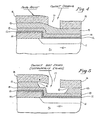
- a photoresist layer 16 of Figure 4 is deposited over the BPSG layer 15. Using standard photolithography techniques, a contact opening 17 is defined in the photoresist layer.
- the B P SG layer 15 is etched away at the contact opening as shown in Figure 5.
- This etch step should be isotropic so that undercutting of the photoresist layer such as at regions 18 of Figure 5 results.
- a wet etch using 6 to 1 BHF for 5 minutes is employed. It is necessary that the etching rate of the B P SG layer 15 be faster than the BSG layer 13. This first etching step should not substantially effect the lower B SG layer.
- BSG has an etch rate of approximately 6 angstroms per second in 6 to 1 BH F while the BPSG has an etch rate of approximately 30 angstroms per second in 6 to 1 BHF (23 0 C).
- the etch rate of the BP SG layer 15 is approximately 5 times the etch rate of the B SG layer 13.
- the BSG layer 13 and the thermal oxide layer 12 are then anisotropically etched in a dry (plasma) etch.
- a dry (plasma) etch is important that this etch be anisotropic so that aggressive design parameters can be utilized.
- the thickness of the BSG layer at area 21 is not substantially effected by this. second etch step so that an adequate insulating layer is maintained.
- the photoresist layer is stripped away and a second reflow step takes place to provide a better profile for metal coverage.
- This second reflow step is performed in nitrogen in the preferred embodiment at approximately 920°C for approximately 10 minutes. This results in the profile as shown in Figure 7. Because the reflow temperature of the BSG layer 13 is higher than that of BPSG layer 15, there is no substantial thinning of layer 13 at critical area 21. However, at area 20 of layer 15 the second reflow step results in a gradual profile.
- the metal layer is deposited in the contact opening. Good metal coverage is achieved because of the gentle two step contact profile, and adequate insulation between the gate and the metal layer is maintained.
- thermostabilization step is employed following the deposition of the BSG layer 13.
- the devices are heated to 920°C for approximately 5 minutes in order to densify the BSG film and prevent the possible moisture absorption problems.
- the thermostabilization step is not employed, the BSG and BPSG layers can be applied in a single sequential step.
- the method of forming contacts of the present invention is also advantageously employed when forming contact openings at a junction which is next to field oxide region.
- An example is shown in Figures 8 and 9.
- a BSG layer 13 and BPSG layer 15 have been formed on a silicon substrate which includes the field oxide region 22.
- the field oxide region includes a "birds beak" region 29, a tapered extension of the oxide along the substrate.
- a photoresist layer 16 is formed thereon and an opening is defined.
- the lower BSG layer 13 is anisotropically plasma etched.
Landscapes
- Internal Circuitry In Semiconductor Integrated Circuit Devices (AREA)
- Electrodes Of Semiconductors (AREA)
- Local Oxidation Of Silicon (AREA)
- Formation Of Insulating Films (AREA)
Applications Claiming Priority (2)
| Application Number | Priority Date | Filing Date | Title |
|---|---|---|---|
| US81752386A | 1986-01-09 | 1986-01-09 | |
| US817523 | 1986-01-09 |
Publications (3)
| Publication Number | Publication Date |
|---|---|
| EP0232508A2 true EP0232508A2 (de) | 1987-08-19 |
| EP0232508A3 EP0232508A3 (en) | 1988-04-06 |
| EP0232508B1 EP0232508B1 (de) | 1992-03-11 |
Family
ID=25223263
Family Applications (1)
| Application Number | Title | Priority Date | Filing Date |
|---|---|---|---|
| EP86117137A Expired - Lifetime EP0232508B1 (de) | 1986-01-09 | 1986-12-09 | Verfahren zur Herstellung eines Kontakts unter Verwendung der Erweichung zweier Glasschichten |
Country Status (5)
| Country | Link |
|---|---|
| US (1) | US4824767A (de) |
| EP (1) | EP0232508B1 (de) |
| JP (1) | JP2587626B2 (de) |
| KR (1) | KR950000096B1 (de) |
| DE (1) | DE3684298D1 (de) |
Cited By (6)
| Publication number | Priority date | Publication date | Assignee | Title |
|---|---|---|---|---|
| EP0369336A3 (de) * | 1988-11-14 | 1990-08-22 | National Semiconductor Corporation | Prozess zur Herstellung von Bipolar- und CMOS-Transistoren auf einem gemeinsamen Substrat |
| US5164340A (en) * | 1991-06-24 | 1992-11-17 | Sgs-Thomson Microelectronics, Inc | Structure and method for contacts in cmos devices |
| EP0534130A1 (de) * | 1991-09-26 | 1993-03-31 | Siemens Aktiengesellschaft | Verfahren zur Herstellung einer selbstjustierten Kontaklochanordnung und selbstjustierte Kontaktlochanordnung |
| EP0450572A3 (en) * | 1990-04-05 | 1994-06-01 | Ramtron Int Corp | Sealed self aligned contact process and structure |
| US5610099A (en) * | 1994-06-28 | 1997-03-11 | Ramtron International Corporation | Process for fabricating transistors using composite nitride structure |
| CN101960565B (zh) * | 2008-02-28 | 2012-09-05 | 惠普开发有限公司 | 半导体基板接触通孔 |
Families Citing this family (28)
| Publication number | Priority date | Publication date | Assignee | Title |
|---|---|---|---|---|
| JPH0793354B2 (ja) * | 1988-11-28 | 1995-10-09 | 株式会社東芝 | 半導体装置の製造方法 |
| US4885262A (en) * | 1989-03-08 | 1989-12-05 | Intel Corporation | Chemical modification of spin-on glass for improved performance in IC fabrication |
| KR920004541B1 (ko) * | 1989-05-30 | 1992-06-08 | 현대전자산업 주식회사 | 반도체 소자에서 식각베리어층을 사용한 콘택홀 형성방법 |
| US5275972A (en) * | 1990-02-19 | 1994-01-04 | Matsushita Electric Industrial Co., Ltd. | Method for fabricating a semiconductor integrated circuit device including the self-aligned formation of a contact window |
| JPH04186657A (ja) * | 1990-11-16 | 1992-07-03 | Sharp Corp | コンタクト配線の作製方法 |
| US5246883A (en) * | 1992-02-06 | 1993-09-21 | Sgs-Thomson Microelectronics, Inc. | Semiconductor contact via structure and method |
| US5308415A (en) * | 1992-12-31 | 1994-05-03 | Chartered Semiconductor Manufacturing Pte Ltd. | Enhancing step coverage by creating a tapered profile through three dimensional resist pull back |
| US5702870A (en) * | 1993-08-27 | 1997-12-30 | Vlsi Technology, Inc. | Integrated-circuit via formation using gradient photolithography |
| US5435888A (en) * | 1993-12-06 | 1995-07-25 | Sgs-Thomson Microelectronics, Inc. | Enhanced planarization technique for an integrated circuit |
| US6107194A (en) * | 1993-12-17 | 2000-08-22 | Stmicroelectronics, Inc. | Method of fabricating an integrated circuit |
| EP0660392A1 (de) | 1993-12-17 | 1995-06-28 | STMicroelectronics, Inc. | Verfahren und Struktur der dielektrischen Zwischenschicht zur verbesserten metallischen Stufenbeschichtung |
| US6284584B1 (en) | 1993-12-17 | 2001-09-04 | Stmicroelectronics, Inc. | Method of masking for periphery salicidation of active regions |
| US5439846A (en) * | 1993-12-17 | 1995-08-08 | Sgs-Thomson Microelectronics, Inc. | Self-aligned method for forming contact with zero offset to gate |
| US6025277A (en) * | 1997-05-07 | 2000-02-15 | United Microelectronics Corp. | Method and structure for preventing bonding pad peel back |
| US6271117B1 (en) * | 1997-06-23 | 2001-08-07 | Vanguard International Semiconductor Corporation | Process for a nail shaped landing pad plug |
| JP4093395B2 (ja) * | 2001-08-03 | 2008-06-04 | 富士通株式会社 | 半導体装置とその製造方法 |
| TW569077B (en) * | 2003-05-13 | 2004-01-01 | Univ Nat Chiao Tung | Method for fabricating nanometer gate in semiconductor device using thermally reflowed resist technology |
| TWI220770B (en) * | 2003-06-11 | 2004-09-01 | Ind Tech Res Inst | Method for forming a conductive layer |
| US20050098480A1 (en) * | 2003-11-12 | 2005-05-12 | Robert Galiasso | Hydrotreating catalyst and method |
| US8878245B2 (en) | 2006-11-30 | 2014-11-04 | Cree, Inc. | Transistors and method for making ohmic contact to transistors |
| US8368100B2 (en) * | 2007-11-14 | 2013-02-05 | Cree, Inc. | Semiconductor light emitting diodes having reflective structures and methods of fabricating same |
| US9634191B2 (en) * | 2007-11-14 | 2017-04-25 | Cree, Inc. | Wire bond free wafer level LED |
| KR101004842B1 (ko) | 2008-07-25 | 2010-12-28 | 삼성전기주식회사 | 전자 칩 모듈 |
| US8384115B2 (en) * | 2008-08-01 | 2013-02-26 | Cree, Inc. | Bond pad design for enhancing light extraction from LED chips |
| US8741715B2 (en) * | 2009-04-29 | 2014-06-03 | Cree, Inc. | Gate electrodes for millimeter-wave operation and methods of fabrication |
| US9070851B2 (en) | 2010-09-24 | 2015-06-30 | Seoul Semiconductor Co., Ltd. | Wafer-level light emitting diode package and method of fabricating the same |
| USD826871S1 (en) | 2014-12-11 | 2018-08-28 | Cree, Inc. | Light emitting diode device |
| CN205944139U (zh) | 2016-03-30 | 2017-02-08 | 首尔伟傲世有限公司 | 紫外线发光二极管封装件以及包含此的发光二极管模块 |
Family Cites Families (5)
| Publication number | Priority date | Publication date | Assignee | Title |
|---|---|---|---|---|
| US4372034B1 (en) * | 1981-03-26 | 1998-07-21 | Intel Corp | Process for forming contact openings through oxide layers |
| US4363830A (en) * | 1981-06-22 | 1982-12-14 | Rca Corporation | Method of forming tapered contact holes for integrated circuit devices |
| JPS6092623A (ja) * | 1983-10-26 | 1985-05-24 | Nec Corp | 半導体装置の製造方法 |
| US4508815A (en) * | 1983-11-03 | 1985-04-02 | Mostek Corporation | Recessed metallization |
| JPS60198847A (ja) * | 1984-03-23 | 1985-10-08 | Nec Corp | 半導体装置およびその製造方法 |
-
1986
- 1986-12-09 DE DE8686117137T patent/DE3684298D1/de not_active Expired - Lifetime
- 1986-12-09 EP EP86117137A patent/EP0232508B1/de not_active Expired - Lifetime
-
1987
- 1987-01-08 KR KR1019870000090A patent/KR950000096B1/ko not_active Expired - Lifetime
- 1987-01-09 JP JP62001952A patent/JP2587626B2/ja not_active Expired - Lifetime
- 1987-06-02 US US07/057,240 patent/US4824767A/en not_active Expired - Lifetime
Cited By (9)
| Publication number | Priority date | Publication date | Assignee | Title |
|---|---|---|---|---|
| EP0369336A3 (de) * | 1988-11-14 | 1990-08-22 | National Semiconductor Corporation | Prozess zur Herstellung von Bipolar- und CMOS-Transistoren auf einem gemeinsamen Substrat |
| US5554554A (en) * | 1988-11-14 | 1996-09-10 | National Semiconductor Corporation | Process for fabricating two loads having different resistance levels in a common layer of polysilicon |
| EP0450572A3 (en) * | 1990-04-05 | 1994-06-01 | Ramtron Int Corp | Sealed self aligned contact process and structure |
| US5385634A (en) * | 1990-04-05 | 1995-01-31 | Ramtron International Corporation | Sealed self aligned contact process |
| US5164340A (en) * | 1991-06-24 | 1992-11-17 | Sgs-Thomson Microelectronics, Inc | Structure and method for contacts in cmos devices |
| EP0534130A1 (de) * | 1991-09-26 | 1993-03-31 | Siemens Aktiengesellschaft | Verfahren zur Herstellung einer selbstjustierten Kontaklochanordnung und selbstjustierte Kontaktlochanordnung |
| US5610099A (en) * | 1994-06-28 | 1997-03-11 | Ramtron International Corporation | Process for fabricating transistors using composite nitride structure |
| CN101960565B (zh) * | 2008-02-28 | 2012-09-05 | 惠普开发有限公司 | 半导体基板接触通孔 |
| US8476742B2 (en) | 2008-02-28 | 2013-07-02 | Hewlett-Packard Development Company, L.P. | Fluid ejection device comprising substrate contact via |
Also Published As
| Publication number | Publication date |
|---|---|
| US4824767A (en) | 1989-04-25 |
| EP0232508A3 (en) | 1988-04-06 |
| KR870007566A (ko) | 1987-08-20 |
| EP0232508B1 (de) | 1992-03-11 |
| DE3684298D1 (de) | 1992-04-16 |
| KR950000096B1 (ko) | 1995-01-09 |
| JPS62160743A (ja) | 1987-07-16 |
| JP2587626B2 (ja) | 1997-03-05 |
Similar Documents
| Publication | Publication Date | Title |
|---|---|---|
| EP0232508B1 (de) | Verfahren zur Herstellung eines Kontakts unter Verwendung der Erweichung zweier Glasschichten | |
| US4714686A (en) | Method of forming contact plugs for planarized integrated circuits | |
| US4795718A (en) | Self-aligned contact for MOS processing | |
| US4305760A (en) | Polysilicon-to-substrate contact processing | |
| JPH08102449A (ja) | 有機含有誘電率材料を用いた自己整合コンタクト | |
| JPS61107727A (ja) | 半導体装置に金属コンタクト・スタツドを形成する方法 | |
| JP2886494B2 (ja) | 集積回路チップの製造方法 | |
| KR100270464B1 (ko) | 함몰형 산화절연을 형성하는 방법 | |
| US5872056A (en) | Semiconductor processing methods of forming self-aligned contact openings | |
| US6040221A (en) | Semiconductor processing methods of forming a buried contact, a conductive line, an electrical connection to a buried contact area, and a field effect transistor gate | |
| EP0121351B1 (de) | Verfahren zum Herstellen von MOS-Halbleiterbauelementen | |
| JPH11186225A (ja) | テーパ形コンタクトホールの形成方法、テーパ形ポリシリコンプラグの形成方法並びにテーパ形ポリシリコンプラグ | |
| US5894169A (en) | Low-leakage borderless contacts to doped regions | |
| EP0081226A2 (de) | Verfahren zur Herstellung einer Halbleiteranordnung | |
| JPH03138930A (ja) | ポリシリコン・ウィンドーパッドを有する電界効果トランジスタ | |
| KR100209280B1 (ko) | 반도체 소자의 콘택홀 형성방법 | |
| US5620911A (en) | Method for fabricating a metal field effect transistor having a recessed gate | |
| US5691250A (en) | Method of forming a metal contact to a novel polysilicon contact extension | |
| US20030006487A1 (en) | Semiconductor device having element isolation structure | |
| KR0162144B1 (ko) | 반도체 소자의 콘택홀 형성 방법 | |
| KR100219549B1 (ko) | 랜딩 패드를 갖는 반도체 소자의 제조방법 | |
| JPH05226466A (ja) | 半導体装置の製造方法 | |
| KR960016236B1 (ko) | 반도체 장치의 자기 정렬형 콘택 제조방법 | |
| KR920005390B1 (ko) | 접촉창 형성방법 | |
| KR0147424B1 (ko) | 반도체 장치의 자기정렬 콘택 형성방법 |
Legal Events
| Date | Code | Title | Description |
|---|---|---|---|
| PUAI | Public reference made under article 153(3) epc to a published international application that has entered the european phase |
Free format text: ORIGINAL CODE: 0009012 |
|
| AK | Designated contracting states |
Kind code of ref document: A2 Designated state(s): DE FR GB IT |
|
| 17P | Request for examination filed |
Effective date: 19871202 |
|
| PUAL | Search report despatched |
Free format text: ORIGINAL CODE: 0009013 |
|
| AK | Designated contracting states |
Kind code of ref document: A3 Designated state(s): DE FR GB IT |
|
| 17Q | First examination report despatched |
Effective date: 19900515 |
|
| GRAA | (expected) grant |
Free format text: ORIGINAL CODE: 0009210 |
|
| AK | Designated contracting states |
Kind code of ref document: B1 Designated state(s): DE FR GB IT |
|
| PG25 | Lapsed in a contracting state [announced via postgrant information from national office to epo] |
Ref country code: IT Free format text: LAPSE BECAUSE OF FAILURE TO SUBMIT A TRANSLATION OF THE DESCRIPTION OR TO PAY THE FEE WITHIN THE PRESCRIBED TIME-LIMIT;WARNING: LAPSES OF ITALIAN PATENTS WITH EFFECTIVE DATE BEFORE 2007 MAY HAVE OCCURRED AT ANY TIME BEFORE 2007. THE CORRECT EFFECTIVE DATE MAY BE DIFFERENT FROM THE ONE RECORDED. Effective date: 19920311 |
|
| REF | Corresponds to: |
Ref document number: 3684298 Country of ref document: DE Date of ref document: 19920416 |
|
| ET | Fr: translation filed | ||
| PLBE | No opposition filed within time limit |
Free format text: ORIGINAL CODE: 0009261 |
|
| STAA | Information on the status of an ep patent application or granted ep patent |
Free format text: STATUS: NO OPPOSITION FILED WITHIN TIME LIMIT |
|
| 26N | No opposition filed | ||
| REG | Reference to a national code |
Ref country code: GB Ref legal event code: IF02 |
|
| PGFP | Annual fee paid to national office [announced via postgrant information from national office to epo] |
Ref country code: GB Payment date: 20031202 Year of fee payment: 18 |
|
| PGFP | Annual fee paid to national office [announced via postgrant information from national office to epo] |
Ref country code: FR Payment date: 20031218 Year of fee payment: 18 |
|
| PGFP | Annual fee paid to national office [announced via postgrant information from national office to epo] |
Ref country code: DE Payment date: 20041124 Year of fee payment: 19 |
|
| PG25 | Lapsed in a contracting state [announced via postgrant information from national office to epo] |
Ref country code: GB Free format text: LAPSE BECAUSE OF NON-PAYMENT OF DUE FEES Effective date: 20041209 |
|
| GBPC | Gb: european patent ceased through non-payment of renewal fee |
Effective date: 20041209 |
|
| PG25 | Lapsed in a contracting state [announced via postgrant information from national office to epo] |
Ref country code: FR Free format text: LAPSE BECAUSE OF NON-PAYMENT OF DUE FEES Effective date: 20050831 |
|
| REG | Reference to a national code |
Ref country code: FR Ref legal event code: ST |
|
| PG25 | Lapsed in a contracting state [announced via postgrant information from national office to epo] |
Ref country code: DE Free format text: LAPSE BECAUSE OF NON-PAYMENT OF DUE FEES Effective date: 20060701 |