EP0232859A2 - Réseau d'intercommunication pour processeurs - Google Patents
Réseau d'intercommunication pour processeurs Download PDFInfo
- Publication number
- EP0232859A2 EP0232859A2 EP87101583A EP87101583A EP0232859A2 EP 0232859 A2 EP0232859 A2 EP 0232859A2 EP 87101583 A EP87101583 A EP 87101583A EP 87101583 A EP87101583 A EP 87101583A EP 0232859 A2 EP0232859 A2 EP 0232859A2
- Authority
- EP
- European Patent Office
- Prior art keywords
- processors
- processor
- receiving
- address
- sending
- Prior art date
- Legal status (The legal status is an assumption and is not a legal conclusion. Google has not performed a legal analysis and makes no representation as to the accuracy of the status listed.)
- Ceased
Links
Images




Classifications
-
- G—PHYSICS
- G06—COMPUTING OR CALCULATING; COUNTING
- G06F—ELECTRIC DIGITAL DATA PROCESSING
- G06F15/00—Digital computers in general; Data processing equipment in general
- G06F15/16—Combinations of two or more digital computers each having at least an arithmetic unit, a program unit and a register, e.g. for a simultaneous processing of several programs
- G06F15/163—Interprocessor communication
- G06F15/173—Interprocessor communication using an interconnection network, e.g. matrix, shuffle, pyramid, star, snowflake
- G06F15/17356—Indirect interconnection networks
- G06F15/17368—Indirect interconnection networks non hierarchical topologies
- G06F15/17381—Two dimensional, e.g. mesh, torus
Definitions
- the present invention relates to an intercommunication network for the transmission of signals, or orders, between processors in a multiprocessor system.
- the present invention as claimed provides a communication network for transmission of such orders between processors of a multiprocessor system.
- every pair of processors is connected by a separate path for carrying the multi-bit orders so that in an N processor multiprocessing system there are N-1 bidirectional communication paths to and from each of the N processors.
- To send an order from one processor to another processor each of the N processors has a routing circuit to select the proper path to that other processor.
- the routing circuit compares the sender's own address to the address of the intended receiver to select the appropriate path.
- Each of the N processors also has a receiving circuit to block orders from any one of the other N-1 processors. In blocking orders, these receiving circuits use the receiver's address to determine which one of the N-1 paths into the receiver is from that any one processor.
- the logic of the routing and receiving circuits permits the identical circuits to be used for these purposes in each of the N processors. In addition, it is possible to change the addresses of the N processors without having to change the communication network coupling the processors and the routing and receiving circuits in the processors. Furthermore, the logic of the routing and receiving circuits does not require the addresses of the routing and/or receiving circuit to be transmitted along with the 2-bit order.
- Fig. 1 shows a 6-way multiprocessor system in which the six processors 0, 1, 2, 3, 4 and 5 are divided into two groups of three processors each. Any one of the six processors can transmit an order to itself or any of the other five processors along a separate multi-line path that connects only the sending and the receiving processor together. For purposes of this description control processor "0" will assumed to be the transmitting processor. Then, processors 0, 1 and 2 make up the local processor group 10 while processors 3, 4 and 5 make up the remote processor group 12. Each processor has five terminal ports A, B, C, D and E, for connecting five, four-line communication paths to that processor. Each four-line path is divided into two unidirectional buses of two lines each, for carrying a two-bit encoded order between the two processors linked by that path. The two-bit binary coded order indicates a type of function to be performed by the receiving processor.
- each processor interfaces with each of the other two processors in the same group directly through a cable 14 containing one of the four-line paths.
- These are identical flat cables with two of the cables given a 1/2 twist to reverse the connections so that like interfacing port connectors in each processor are wired alike instead of as mirror images of each other.
- Each processor also interfaces the processors in the remote group through twelve wire flat cables 16, each containing three four-wire paths, one for each of the processors in the remote group.
- the four-wire paths in cables 16 pass through an interconnection terminal 24 which is schematically illustrated in Fig. 3.
- the terminal 24 is wired so the connectors in the processors can be wired identically instead of being mirror images of each other.
- each of the processors 0, 1, 2, 3, 4, 5 there is logic circuits for sending and receiving.
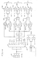
- the sending logic circuit shown in Figs. 4A and 4B routes the 2-bit binary coded order onto the output unidirectional 2-bit bus of one of the terminal ports A, B, C, D, E for transmission.
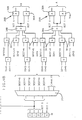
- the receiving circuit of Figs. 5A and 5B enables the receipt of the 2-bit signal into the processor on the input unidirectional buses connected to the terminal ports A, B, C, D and E.
- the gating of the outgoing orders is done on the basis of a 3 binary bit identifier of both the transmitting device and the receiving device. For instance, if processor 0 whose address is 000 is transmitting to device 1 whose address is 001, both IDs affect which terminal (port A) the order is being transmitted out onto.
- the gating of incoming orders involves the receiving ID (001) which identifies the terminal (port A) the order is received on.
- the table of Fig. 6 is a truth table which shows the port used in sending or receiving an order. In case of sending an order, the numbers in the top row of the table represent the ID of the sending processor. In the case of receiving an order, the numbers in the top row represent the receiving processor. For instance, if an order is to be sent by processor 1 to processor 2, it is transmitted out of processor 1 on terminal port B as shown by dotted line 50 and received by processor 2 at terminal port A as shown by dotted line 52.
- the logic circuitry in each processor includes two registers, an ID register 20 which contains the ID or address of the processor containing the logic circuit and a signal processor (SIG-P) register 22 which contains both the ID or address of the processor to which a message is to be sent and the 2-bit encoded message being sent to that processor.
- the ID's are three bit binary numbers which are the binary equivalents of the decimal number assigned to the processor in Fig. 1. Thus, the ID of processor 0 is 000, the ID of processor 1 is 001 and so on.
- the order is a 2 bit binary number representing the type of function to be performed by the processor receiving the order.
- the 3-bit IDs in both registers 20 and 22 are decoded by decoders 26 and 27 respectively to select one of 8 possible decoder outputs. Two of the outputs (6 and 7) of both the decoders are unused or invalid outputs in this 6-way processor configuration.
- gate 28E is enabled by the output of OR gate 36E the other gates 28A - 28D are not enabled so that the order is not transmitted to any processor except processor 0.
- the ID data in registers 20 and 22 is fed into address comparator 38. If the IDs are identical, the output of comparator 38 enables gate 28′ which feeds the order data bit 0 and bit 1 back into the sending processor, or in other words wraps the data.
- gates 40 control the reception of data into the processor. Gates 40 each control the entry of order bits 0′ and 1′ through one of the ports. Before the order can enter through any gate 40, the gate 40 must receive an enabling output from its associated OR gate 42. In order for this enabling signal to be produced, AND gates have to receive an ID output of the decoder 26 and a not blocked pulse (ex B1K2). Therefore, each processor can selectively block an order from any of the five other processors by dropping the non-blocking pulse for that processor. The processor ID then identifies which port receives signals from that processor. For instance, suppose processor 0 decides it does not want to receive an order from processor 4. Then B1K4 goes down disabling gate 40D and thereby blocking incoming order bits 0′ and 1′ from entering on port D. An examination of the table on Fig 6 shows that order signals from processor 4 are received at port D in processor 0.
- circuit has been described. A number of changes can be made in this embodiment. For instance, six processors need not be employed to have the system operate. Any of the processors can be missing but the system will still function with respect to the remaining processors. Also, while the coding permits eight processors, the system shown here has been developed for only six. Obviously, the invalid output of the decoders 26 and 27 could be used if the system were expanded to include eight processors. Furthermore, by increasing the number of bits in the processor's ID or addresses and appropriately modifying the transmission network, the system could include even more than eight processors.
Landscapes
- Engineering & Computer Science (AREA)
- Physics & Mathematics (AREA)
- Computer Hardware Design (AREA)
- Theoretical Computer Science (AREA)
- Mathematical Physics (AREA)
- Software Systems (AREA)
- General Engineering & Computer Science (AREA)
- General Physics & Mathematics (AREA)
- Multi Processors (AREA)
- Computer And Data Communications (AREA)
Applications Claiming Priority (2)
| Application Number | Priority Date | Filing Date | Title |
|---|---|---|---|
| US06/823,103 US4697171A (en) | 1985-03-25 | 1986-01-27 | Electronic lock and key |
| US823103 | 1992-01-21 |
Publications (2)
| Publication Number | Publication Date |
|---|---|
| EP0232859A2 true EP0232859A2 (fr) | 1987-08-19 |
| EP0232859A3 EP0232859A3 (fr) | 1989-08-30 |
Family
ID=25237807
Family Applications (1)
| Application Number | Title | Priority Date | Filing Date |
|---|---|---|---|
| EP87101583A Ceased EP0232859A3 (fr) | 1986-01-27 | 1987-02-05 | Réseau d'intercommunication pour processeurs |
Country Status (1)
| Country | Link |
|---|---|
| EP (1) | EP0232859A3 (fr) |
Cited By (7)
| Publication number | Priority date | Publication date | Assignee | Title |
|---|---|---|---|---|
| GB2212308A (en) * | 1987-11-11 | 1989-07-19 | Toshiba Kk | Method and apparatus for parallel computation |
| GB2232512A (en) * | 1989-05-31 | 1990-12-12 | Plessey Telecomm | Processor unit networks |
| EP0600114A1 (fr) * | 1992-11-30 | 1994-06-08 | Siemens Nixdorf Informationssysteme Aktiengesellschaft | Réseau de connection pour échange d'information entre des unités de commande |
| WO1996026491A1 (fr) * | 1995-02-22 | 1996-08-29 | Callisto Media Systems Inc. | Serveur multimedia |
| EP0744851A1 (fr) * | 1995-05-24 | 1996-11-27 | International Business Machines Corporation | Système de traitement de données distribué |
| EP0860017A4 (fr) * | 1995-10-24 | 2001-02-28 | Seachange International Inc | Groupement a couplage lache d'ordinateurs dotes de memoires de grande capacite |
| US6449730B2 (en) | 1995-10-24 | 2002-09-10 | Seachange Technology, Inc. | Loosely coupled mass storage computer cluster |
Family Cites Families (4)
| Publication number | Priority date | Publication date | Assignee | Title |
|---|---|---|---|---|
| US3680052A (en) * | 1970-02-20 | 1972-07-25 | Ibm | Configuration control of data processing system units |
| IT1111606B (it) * | 1978-03-03 | 1986-01-13 | Cselt Centro Studi Lab Telecom | Sistema elaborativo modulare multiconfigurabile integrato con un sistema di preelaborazione |
| DE2920994A1 (de) * | 1979-05-23 | 1980-11-27 | Siemens Ag | Datensende/-empfangseinrichtung mit parallel/seriell- und seriell/parallel- zeichenumsetzung, insbesondere zum datenaustausch zwischen kommunizierenden datenverarbeitungsanlagen |
| US4724517A (en) * | 1982-11-26 | 1988-02-09 | Inmos Limited | Microcomputer with prefixing functions |
-
1987
- 1987-02-05 EP EP87101583A patent/EP0232859A3/fr not_active Ceased
Cited By (13)
| Publication number | Priority date | Publication date | Assignee | Title |
|---|---|---|---|---|
| GB2212308A (en) * | 1987-11-11 | 1989-07-19 | Toshiba Kk | Method and apparatus for parallel computation |
| US4893303A (en) * | 1987-11-11 | 1990-01-09 | Kabushiki Kaisha Toshiba | Method and apparatus for parallel computation |
| GB2212308B (en) * | 1987-11-11 | 1992-04-22 | Toshiba Kk | Method and apparatus for parallel computation |
| GB2232512A (en) * | 1989-05-31 | 1990-12-12 | Plessey Telecomm | Processor unit networks |
| EP0600114A1 (fr) * | 1992-11-30 | 1994-06-08 | Siemens Nixdorf Informationssysteme Aktiengesellschaft | Réseau de connection pour échange d'information entre des unités de commande |
| WO1996026491A1 (fr) * | 1995-02-22 | 1996-08-29 | Callisto Media Systems Inc. | Serveur multimedia |
| EP0744851A1 (fr) * | 1995-05-24 | 1996-11-27 | International Business Machines Corporation | Système de traitement de données distribué |
| EP0860017A4 (fr) * | 1995-10-24 | 2001-02-28 | Seachange International Inc | Groupement a couplage lache d'ordinateurs dotes de memoires de grande capacite |
| US6449730B2 (en) | 1995-10-24 | 2002-09-10 | Seachange Technology, Inc. | Loosely coupled mass storage computer cluster |
| US6557114B2 (en) | 1995-10-24 | 2003-04-29 | Seachange Technology, Inc. | Loosely coupled mass storage computer cluster |
| US6571349B1 (en) | 1995-10-24 | 2003-05-27 | Seachange Technology, Inc. | Loosely coupled mass storage computer cluster |
| US6574745B2 (en) | 1995-10-24 | 2003-06-03 | Seachange International, Inc. | Loosely coupled mass storage computer cluster |
| US8019941B2 (en) | 1995-10-24 | 2011-09-13 | Seachange International, Inc. | Loosely coupled mass storage computer cluster having a set of data storage controllers interoperable for reading and writing data objects |
Also Published As
| Publication number | Publication date |
|---|---|
| EP0232859A3 (fr) | 1989-08-30 |
Similar Documents
| Publication | Publication Date | Title |
|---|---|---|
| EP0018755B1 (fr) | Réseaux de communication digitale, utilisant des commutateurs indépendants de la vitesse | |
| CA1258113A (fr) | Reseau a commutation de paquets a destinations multiples | |
| US4082922A (en) | Statistical multiplexing system for computer communications | |
| US5206946A (en) | Apparatus using converters, multiplexer and two latches to convert SCSI data into serial data and vice versa | |
| US4339633A (en) | Modular telecommunications system | |
| US4783657A (en) | Processor intercommunication network | |
| EP0018756B1 (fr) | Interrupteur d'arbitrage indépendant de la vitesse pour réseaux de communication digitaux | |
| CA1253243A (fr) | Central de telecommunication attribuant des largeurs de bande variables aux canaux | |
| JPS6340383B2 (fr) | ||
| ES8401294A1 (es) | "un sistema de diagnostico para una red de conmutacion con control distribuido". | |
| EP0232859A2 (fr) | Réseau d'intercommunication pour processeurs | |
| EP0621709B1 (fr) | Système de communication des messages | |
| US3947818A (en) | Bus-coupler | |
| WO1984001079A1 (fr) | Commutateur d'arbitrage a quatre voies pour un module a cinq ports faisant office de noeud dans un reseau asynchrone independant de la vitesse de processeurs fonctionnant en simultaneite | |
| US4584680A (en) | Use of a tone bus to provide polling and data distribution apparatus for communication system terminal groups | |
| JPS6410977B2 (fr) | ||
| CA2177781C (fr) | Central prive numerique a systeme de controle multiprocesseur utilisant un mode de transfert asynchrone | |
| US5592484A (en) | Telecommunication network having a number of stations which are connected to a token ring network, and station for such a network | |
| US5056012A (en) | Memory addressable data transfer network | |
| GB2128850A (en) | Time slot assignment facilities | |
| EP0040046A1 (fr) | Système de télécommunication modulaire | |
| US5175728A (en) | Flexible interface system for interfacing different complements of port circuits for a pcm telephony switching system | |
| US4628505A (en) | Signaling terminal system for CCITT No. 7 common channel signaling system | |
| EP0005045A1 (fr) | Système de communication de données par impulsions et adapteur | |
| SU840867A1 (ru) | Устройство дл сопр жени вычислительныхМАшиН |
Legal Events
| Date | Code | Title | Description |
|---|---|---|---|
| PUAI | Public reference made under article 153(3) epc to a published international application that has entered the european phase |
Free format text: ORIGINAL CODE: 0009012 |
|
| AK | Designated contracting states |
Kind code of ref document: A2 Designated state(s): DE FR GB |
|
| 17P | Request for examination filed |
Effective date: 19871211 |
|
| PUAL | Search report despatched |
Free format text: ORIGINAL CODE: 0009013 |
|
| AK | Designated contracting states |
Kind code of ref document: A3 Designated state(s): DE FR GB |
|
| 17Q | First examination report despatched |
Effective date: 19920416 |
|
| STAA | Information on the status of an ep patent application or granted ep patent |
Free format text: STATUS: THE APPLICATION HAS BEEN REFUSED |
|
| 18R | Application refused |
Effective date: 19921010 |
|
| RIN1 | Information on inventor provided before grant (corrected) |
Inventor name: BOUCHARD, STANLEY FREDERICK Inventor name: HEINTZ, PAUL RUSSELL Inventor name: TRACY, PAUL HARRY |