EP0233221B1 - Gerät und verfahren zur erkennung von zeitverwandten fehlern - Google Patents
Gerät und verfahren zur erkennung von zeitverwandten fehlern Download PDFInfo
- Publication number
- EP0233221B1 EP0233221B1 EP86904705A EP86904705A EP0233221B1 EP 0233221 B1 EP0233221 B1 EP 0233221B1 EP 86904705 A EP86904705 A EP 86904705A EP 86904705 A EP86904705 A EP 86904705A EP 0233221 B1 EP0233221 B1 EP 0233221B1
- Authority
- EP
- European Patent Office
- Prior art keywords
- signals
- differential
- bistable
- signal
- clock
- Prior art date
- Legal status (The legal status is an assumption and is not a legal conclusion. Google has not performed a legal analysis and makes no representation as to the accuracy of the status listed.)
- Expired
Links
Images


Classifications
-
- G—PHYSICS
- G06—COMPUTING OR CALCULATING; COUNTING
- G06F—ELECTRIC DIGITAL DATA PROCESSING
- G06F11/00—Error detection; Error correction; Monitoring
- G06F11/07—Responding to the occurrence of a fault, e.g. fault tolerance
- G06F11/0703—Error or fault processing not based on redundancy, i.e. by taking additional measures to deal with the error or fault not making use of redundancy in operation, in hardware, or in data representation
- G06F11/0751—Error or fault detection not based on redundancy
- G06F11/0754—Error or fault detection not based on redundancy by exceeding limits
- G06F11/0757—Error or fault detection not based on redundancy by exceeding limits by exceeding a time limit, i.e. time-out, e.g. watchdogs
-
- G—PHYSICS
- G06—COMPUTING OR CALCULATING; COUNTING
- G06F—ELECTRIC DIGITAL DATA PROCESSING
- G06F1/00—Details not covered by groups G06F3/00 - G06F13/00 and G06F21/00
- G06F1/04—Generating or distributing clock signals or signals derived directly therefrom
- G06F1/10—Distribution of clock signals, e.g. skew
Definitions
- This invention relates generally to an improved fault detection means comprising: differential signal means providing a pair of differential digital signals; first logical circuit means detecting the phase difference between said differential signals and generating output binary signals in response thereto; and second logical circuit means to which the outputs from said first logical circuit means are applied for producing a fault signal when the phase difference between said differential signals exceeds prescribed limits determined by a predetermined amount and a predetermined direction.
- This invention further relates to an improved method for detecting timing faults in a binary signal, said method comprising the steps of: providing a pair of differential binary signals corresponding to said binary signal wherein each of said differential signals changes between a first logical level and a second logical level; detecting the phase difference between said differential signals at a predetermined time and generating output binary signals in response thereto; and logically combining said output binary signals to produce an error indication when the phase difference between said pair of differential signals exceeds a prescribed amount.
- timing variation faults which could produce errors, particularly in clock generation and distribution circuitry, presents a particularly difficult problem.
- testing for such faults is provided off-line, since the provision of known on-line fault detecting circuitry for this purpose (in order to provide fault detection during actual operation) has been found to not only be expensive, but also to undesirably increase circuit complexity, and may additionally degrade operating speed.
- a more specific object in accordance with the foregoing object is to provide for the on-line detection of faults related to signal timing variations.
- a still more specific object of the invention in accordance with the foregoing objects is to provide improved means and methods for providing highly accurate on-line detection of clocking signal faults.
- An additional object of the invention is to provide for implementing the foregoing objects in a relatively simple and economical manner.
- the above fault detection means is characterized in that said first logical circuit means includes a plurality of bistable means each having a data input, a clock input and at least one output, each bistable means being operative in response to a predetermined change in a signal applied to its clock input to provide a signal at its output indicative of the logical level of the signal applied to its data input when said predetermined change occurs; and coupling means coupling said pair of differential digital signals to the clock and data inputs of each bistable means such that the differential signal applied to one input is delayed by said predetermined amount and in said predetermined direction relative to the differential signal applied to the other input, the coupling provided by said coupling means being chosen so that the signals produced at the outputs of said bistable means are indicative of whether the phase difference between said differential signals is within said prescribed limits.
- the above method for detecting timing faults in a binary signal is characterized by the further steps of delaying said differential signals so as to produce first, second, third and fourth binary signals such that said first and second binary signals have a relative delay therebetween in one direction and said third and fourth binary signals have a relative delay therebetween in an opposite direction, the amount of said relative delays corresponding to said prescribed amount of said phase difference between said pair of differential signals; and detecting the phase relationship between said first and second binary signals and the phase relationship between said third and fourth binary signals in response to the logical levels thereof at a predetermined time and producing said output binary signals in response thereto.
- the above objects are accomplished by taking advantage of the differential signal distribution design commonly employed in many clock distribution systems for such purposes as providing high speed operation, reducing electromagnetic radiation, and increasing noise immunity.
- the already available differential signal design is employed for the additional purpose of providing on-line clock fault detection, whereby very accurate high-speed, on-line fault detection of distributed clock signals is simply provided at low cost.
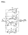
- FIG. 1 is a schematic electric diagram illustrating a particular preferred embodiment of the invention.
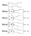
- FIGS. 2a-2e are graphs illustrating the operation of FIG. 1 when the differential clock signals C+ and C_ are in phase.
- FIGS. 3a-3e are graphs illustrating the operation of FIG. 1 for the condition where the clock signal C_ leads the clock signal C+ by more than the prescribed delay "d".
- FIGS. 4a-4e are graphs illustrating the operation of FIG. 1 for the condition where the clock signal C_ lags the clock signal C+ by more than the prescribed delay "d".
- a clock signal is usually distributed to every element capable of holding state (such as flip-flops). Ideally, this clock signal should arrive at every destination simultaneously for proper system functioning. Since this is impossible in the absolute sense, a number of problems can occur.
- race problems can usually be fixed, the solution usually increases system complexity and cost, and may also degrade system speed. Worse, race problems which are unknown to the designer may turn up during manufacture of subsequent systems or during use by the end user, degrading system reliability. Problems such as these make it readily apparent why the provision of fault detection is important in clock generation and distribution systems.
- the fault detection provided should not only be very accurate, but should also be implementable at sufficiently low cost to permit incorporation into high-speed fault-tolerant digital systems so that fault detection can be performed on line (that is, during actual system operation).
- differential signal distribution is provided for a variety of reasons, such as for providing higher speed operation, for reducing electromagnetic radiation, and for increasing noise immunity.
- a differentially distributed signal is a signal which is distributed accompanied by a like signal of opposite polarity.
- Such differential signal distribution is commonly employed in clock generation and distribution systems. In such a case, the clock is distributed using a pair of clock lines having like clock signals of opposite polarity.
- FIG. 1 is a particular preferred embodiment of the invention which illustrates how advantage may be taken of an existing differential clock distribution system to provide highly accurate on-line detection of clock faults.
- a differential pair of clock lines As illustrated in FIG. 1, a differential pair of clock lines, indicated by numeral 8, provides a positive polarity clock signal C+ on one line and a negative polarity clock signal C_ on the other line, as typically illustrated in FIG. 2a.
- C+ and C_ In many modern day digital computer systems, it is important that these opposite polarity clock signals C+ and C_ always be in phase to a very high degree of accuracy.
- the particular preferred embodiment illustrated in FIG. 1 provides for highly accurate on-line detection of when the phase difference between the clock signals C+ and C_ exceeds a prescribed amount. For example, in a system employing ECL integrated circuits, the maximum amount by which the phase of the clocks C+ and C_ can differ is typically one-half of a nanosecond.
- FIG. 1 includes four like flip-flops 10, 12, 14 and 16, each having a clock input C, a data input D, an output Q and an inverse output Q .
- each flip-flop operates in response to the positive edge of a signal applied to its clock input C to provide signals on outputs Q and Q indicative of the logical level of the signal applied to its data input D at that time.
- the Q flip-flop output will provide a “true” or “1” output signal, while the Q flip-flop output will provide a “false” or “0” output signal, and “vice versa” when the signal applied to the data input D is "0" or "false”.
- the C+ signal is directly applied to the flip-flop clock input C, while the C_ signal is applied to the flip-flop data input D via a delay element 15.
- the C+ signal is applied to the clock input C via a like delay element 15, while the C_ input is directly applied to the data input D.
- the C+ signal is applied to the data input D via a like delay element 15 while the C_ signal is applied to the clock input C via an inverter 19.
- the C+ signal is directly applied to the data input D, while the C_ signal is applied to the clock input C via a like inverter 19 and a like delay element 15.
- an OR gate 20 receives the Q outputs from flip-flops 12 and 14 and the Q outputs from flip-flops 10 and 16, whereby the output of OR gate 20 will be "true” or "1" whenever the phase difference between C+ and C_ is greater than the delay provided by the delay element 15. Accordingly, in the particular preferred embodiment illustrated in FIG. 1, each delay element 15 is chosen to provide an accurate delay equal to the maximum phase difference which is to be permitted to occur between the differential clock signals C+ and C_. The presence of a "true” or "1" signal at the output of OR gate 20 during operation will thus indicate a clock fault.
- FIG. 2 The operation of FIG. 2 will now be explained with reference to the graphs of FIGS. 2a-2e, FIGS. 3a-3e, and FIGS. 4a-4e.
- a solid line representation of a signal indicates that it is applied to a flip-flop data input D
- a dashed line representation indicates that it is applied to a flip-flop clock input C.
- the delays shown in these figures are exaggerated for greater clarity.
- FIGS. 2a-2e illustrate the differential clock signals C+ and C_ for the condition where there is no phase difference therebetween as shown in FIG. 2a.
- FIG. 2b illustrates the signals dC_ and C+ respectively applied to the data and clock inputs D and C of flip-flop 10
- FIG. 2c illustrates the signals C_ and dC+ respectively applied to the D and C inputs of flip-flop 12
- FIG. 2d illustrates the signals dC+ and iC_ respectively applied to the D and C inputs of flip-flop 14
- FIG. 2e illustrates the C+ and diC_ signals applied to the D and C inputs of flip-flop 16.
- a “d” preceding a clock signal C+ or C_ indicates that the signal has been delayed by the delay element 15, an “i” indicates that the clock signal has been inverted by the inverter 19, and a “di” indicates that the clock signal has been both inverted and delayed.
- the delay introduced by each delay element 15 in FIG. 1 is indicated in FIGS. 2a-2e by the time period labeled "d".
- FIGS. 3a-3e and FIGS. 4a-4e correspond to FIGS. 2b-2e, respectively, except that FIGS. 3a-3e illustrate the condition where C_ leads C+ by more than the prescribed delay "d” (see FIG. 3a), while FIGS. 4a-4e illustrate the condition where C_ lags C+ by more than the prescribed delay "d” (see FIG. 4a).
- FIGS. 3a-3e illustrate the condition where C_ leads C+ by more than the prescribed delay "d” (see FIG. 3a)
- FIGS. 4a-4e illustrate the condition where C_ lags C+ by more than the prescribed delay "d” (see FIG. 4a).
- flip-flops 10 and 16 in FIG. 1 serve to determine when C_ leads C+ by more than the prescribed delay "d", while flip-flops 12 and 14 determine when C_ lags C+ by more than the prescribed delay "d”, thereby establishing a window of acceptability for phase differences between C+ and C_.
- the provision of the additional pair of flip-flops offers the important advantage of guaranteeing that an error will be produced at the output of OR gate 20 even if one of the clock signals C+ or C_ should be lost. For example, if only flip-flops 10 and 12 were employed in FIG.
- the invention is also applicable for providing fault detection for other types of differential signals besides clock signals. Also, where different leading and lagging tolerances are desired, different delays could be provided for the delay elements 15 in FIG. 1.
Landscapes
- Engineering & Computer Science (AREA)
- Theoretical Computer Science (AREA)
- Physics & Mathematics (AREA)
- General Engineering & Computer Science (AREA)
- General Physics & Mathematics (AREA)
- Quality & Reliability (AREA)
- Manipulation Of Pulses (AREA)
Claims (9)
zweiten logischen Schaltungsmitteln (20), an die die Ausgangssignale (Q,
Koppelmittel (15, 19), die das Paar der differentiellen Digitalsignale (C+, C_) an die Takt-(C) und Dateneingägänge (D) der bistabilen Mittel (10, 12, 14, 16) derart übertragen, daß das an den einen Eingang angelegte differentielle Signal um einen bestimmten Betrag und in einer bestimmten Richtung relativ zu dem am anderen Eingang angelegten Differentiellen Signal (C+, C_) verzögert wird, wodurch die von den Koppelmitteln (15, 19) geschaffene Kopplung so gewählt ist, daß die an den Ausgängen (Q,
ein Paar von differentiellen binären Signalen (C+, C_) entsprechend dem binären Signal zu erzeugen, wobei jedes der differentiellen Signale (C+, C_) zwischen einem ersten logischen Wert und einem zweiten logischen Wert wechselt;
die Phasendifferenz zwischen den differentiellen Signalen (C+, C_) zu einer bestimmten Zeit zu erfassen und binäre Ausgangssignale (Q,
die binären Ausgangssignale (Q,
das Phasenverhältnis zwischen den ersten und zweiten binären Signalen und das Phasenverhältnis zwischen den dritten und vierten binären Signalen in Antwort auf deren logische Werte zu einer vorgegebenen Zeit zu erfassen und die binären Ausgangssignale (Q,
Priority Applications (1)
| Application Number | Priority Date | Filing Date | Title |
|---|---|---|---|
| AT86904705T ATE61130T1 (de) | 1985-08-02 | 1986-07-16 | Geraet und verfahren zur erkennung von zeitverwandten fehlern. |
Applications Claiming Priority (2)
| Application Number | Priority Date | Filing Date | Title |
|---|---|---|---|
| US06/761,989 US4686677A (en) | 1985-08-02 | 1985-08-02 | Apparatus and method for detecting time-related faults |
| US761989 | 1985-08-22 |
Publications (2)
| Publication Number | Publication Date |
|---|---|
| EP0233221A1 EP0233221A1 (de) | 1987-08-26 |
| EP0233221B1 true EP0233221B1 (de) | 1991-02-27 |
Family
ID=25063819
Family Applications (1)
| Application Number | Title | Priority Date | Filing Date |
|---|---|---|---|
| EP86904705A Expired EP0233221B1 (de) | 1985-08-02 | 1986-07-16 | Gerät und verfahren zur erkennung von zeitverwandten fehlern |
Country Status (5)
| Country | Link |
|---|---|
| US (1) | US4686677A (de) |
| EP (1) | EP0233221B1 (de) |
| JP (1) | JPH0654474B2 (de) |
| CA (1) | CA1267224A (de) |
| WO (1) | WO1987001220A1 (de) |
Families Citing this family (17)
| Publication number | Priority date | Publication date | Assignee | Title |
|---|---|---|---|---|
| US4920540A (en) * | 1987-02-25 | 1990-04-24 | Stratus Computer, Inc. | Fault-tolerant digital timing apparatus and method |
| US4800564A (en) * | 1986-09-29 | 1989-01-24 | International Business Machines Corporation | High performance clock system error detection and fault isolation |
| US4811343A (en) * | 1987-03-02 | 1989-03-07 | International Business Machines Corporation | On-chip on-line AC and DC clock tree error detection system |
| US4953167A (en) * | 1988-09-13 | 1990-08-28 | Unisys Corporation | Data bus enable verification logic |
| US5081629A (en) * | 1989-05-08 | 1992-01-14 | Unisys Corporation | Fault isolation for multiphase clock signals supplied to dual modules which are checked by comparison using residue code generators |
| JPH06251096A (ja) * | 1993-02-24 | 1994-09-09 | Nec Ic Microcomput Syst Ltd | タイミング検証回路 |
| US5471488A (en) * | 1994-04-05 | 1995-11-28 | International Business Machines Corporation | Clock fault detection circuit |
| US6106828A (en) * | 1996-02-15 | 2000-08-22 | Novo Nordisk A/S | Conjugation of polypeptides |
| US6456138B1 (en) | 1999-04-30 | 2002-09-24 | Bae Systems Information And Electronic Systems Integration, Inc. | Method and apparatus for a single upset (SEU) tolerant clock splitter |
| US6820213B1 (en) | 2000-04-13 | 2004-11-16 | Stratus Technologies Bermuda, Ltd. | Fault-tolerant computer system with voter delay buffer |
| US6687851B1 (en) | 2000-04-13 | 2004-02-03 | Stratus Technologies Bermuda Ltd. | Method and system for upgrading fault-tolerant systems |
| US6691225B1 (en) | 2000-04-14 | 2004-02-10 | Stratus Technologies Bermuda Ltd. | Method and apparatus for deterministically booting a computer system having redundant components |
| US6718474B1 (en) | 2000-09-21 | 2004-04-06 | Stratus Technologies Bermuda Ltd. | Methods and apparatus for clock management based on environmental conditions |
| US7065672B2 (en) | 2001-03-28 | 2006-06-20 | Stratus Technologies Bermuda Ltd. | Apparatus and methods for fault-tolerant computing using a switching fabric |
| US6928583B2 (en) * | 2001-04-11 | 2005-08-09 | Stratus Technologies Bermuda Ltd. | Apparatus and method for two computing elements in a fault-tolerant server to execute instructions in lockstep |
| US6747490B1 (en) * | 2002-12-23 | 2004-06-08 | Intel Corporation | Sampling pulse generation |
| US9607153B2 (en) | 2013-03-13 | 2017-03-28 | Qualcomm Incorporated | Apparatus and method for detecting clock tampering |
Family Cites Families (10)
| Publication number | Priority date | Publication date | Assignee | Title |
|---|---|---|---|---|
| NL166591C (nl) * | 1971-05-18 | 1981-08-17 | Philips Nv | Foutencorrigerend datatransmissiestelsel. |
| US3728624A (en) * | 1972-02-25 | 1973-04-17 | Cit Alcatel | Phase meter for comparing rectangular waves |
| DE2546481C2 (de) * | 1975-10-17 | 1986-03-06 | Robert Bosch Gmbh, 7000 Stuttgart | Überwachungsschaltung für wenigstens zwei Meßwertgeber |
| JPS53108797A (en) * | 1977-03-04 | 1978-09-21 | Matsushita Electric Ind Co Ltd | Phase-discrimination circuit |
| US4291274A (en) * | 1978-11-22 | 1981-09-22 | Tokyo Shibaura Denki Kabushiki Kaisha | Phase detector circuit using logic gates |
| US4267514A (en) * | 1979-02-16 | 1981-05-12 | The United States Of America As Represented By The Secretary Of The Air Force | Digital phase-frequency detector |
| JPS56155426A (en) * | 1980-05-01 | 1981-12-01 | Nec Corp | Checking circuit for clock phase |
| DE3171263D1 (en) * | 1980-12-12 | 1985-08-08 | Philips Electronic Associated | Phase sensitive detector |
| US4362957A (en) * | 1980-12-29 | 1982-12-07 | Gte Automatic Electric Labs Inc. | Clock pulse tolerance verification circuit |
| JPS6096916A (ja) * | 1983-10-31 | 1985-05-30 | Seiko Instr & Electronics Ltd | デイジタル位相検出回路 |
-
1985
- 1985-08-02 US US06/761,989 patent/US4686677A/en not_active Expired - Lifetime
-
1986
- 1986-07-16 JP JP61504057A patent/JPH0654474B2/ja not_active Expired - Lifetime
- 1986-07-16 EP EP86904705A patent/EP0233221B1/de not_active Expired
- 1986-07-16 WO PCT/US1986/001514 patent/WO1987001220A1/en not_active Ceased
- 1986-08-01 CA CA000515259A patent/CA1267224A/en not_active Expired
Also Published As
| Publication number | Publication date |
|---|---|
| US4686677A (en) | 1987-08-11 |
| CA1267224A (en) | 1990-03-27 |
| EP0233221A1 (de) | 1987-08-26 |
| WO1987001220A1 (en) | 1987-02-26 |
| JPS62503132A (ja) | 1987-12-10 |
| JPH0654474B2 (ja) | 1994-07-20 |
Similar Documents
| Publication | Publication Date | Title |
|---|---|---|
| US4686677A (en) | Apparatus and method for detecting time-related faults | |
| US5555213A (en) | Interface circuit, system and method for interfacing an electronic device and a synchronous state machine having different clock speeds | |
| US6240523B1 (en) | Method and apparatus for automatically determining the phase relationship between two clocks generated from the same source | |
| US5537655A (en) | Synchronized fault tolerant reset | |
| JPH0220173B2 (de) | ||
| KR920004336B1 (ko) | 동기검출회로 | |
| US4636656A (en) | Circuit for selectively extending a cycle of a clock signal | |
| EP1237282A1 (de) | Schaltung zur Detektion von Störungen der Periodendauer in einem Taktsignal | |
| US5157673A (en) | Comparison circuit for masking transient differences | |
| US4317053A (en) | High speed synchronization circuit | |
| US4082218A (en) | Potential failure detecting circuit having improved means for detecting transitions in short duration signals | |
| US4500953A (en) | Data transfer abnormality processing system | |
| US6115438A (en) | Method and circuit for detecting a spurious lock signal from a lock detect circuit | |
| US6182237B1 (en) | System and method for detecting phase errors in asics with multiple clock frequencies | |
| US4093851A (en) | Means and methods for detecting the possibility of a failure occurring in the operation of a digital circuit | |
| US6205192B1 (en) | Clock input control circuit | |
| US4669098A (en) | Increased resolution counting circuit | |
| US5294844A (en) | Sampling signal generation circuit | |
| US4818894A (en) | Method and apparatus for obtaining high frequency resolution of a low frequency signal | |
| US6041418A (en) | Race free and technology independent flag generating circuitry associated with two asynchronous clocks | |
| US6819726B2 (en) | Dynamic phase alignment circuit | |
| KR100629538B1 (ko) | 제 1 디지털 신호의 에지와 제 2 디지털 신호의 에지 사이의 시간차를 검출하는 회로 | |
| JPH03171945A (ja) | ディジタルシステム | |
| US5491438A (en) | Synchronized clock generating apparatus | |
| KR100373333B1 (ko) | 비동기전달모드 셀 동기 신호의 오류 검출 장치 |
Legal Events
| Date | Code | Title | Description |
|---|---|---|---|
| PUAI | Public reference made under article 153(3) epc to a published international application that has entered the european phase |
Free format text: ORIGINAL CODE: 0009012 |
|
| 17P | Request for examination filed |
Effective date: 19870331 |
|
| AK | Designated contracting states |
Kind code of ref document: A1 Designated state(s): AT BE CH DE FR GB IT LI LU NL SE |
|
| RBV | Designated contracting states (corrected) |
Designated state(s): AT BE CH DE FR GB LI LU NL SE |
|
| 17Q | First examination report despatched |
Effective date: 19890906 |
|
| RAP1 | Party data changed (applicant data changed or rights of an application transferred) |
Owner name: UNISYS CORPORATION |
|
| GRAA | (expected) grant |
Free format text: ORIGINAL CODE: 0009210 |
|
| AK | Designated contracting states |
Kind code of ref document: B1 Designated state(s): AT BE CH DE FR GB LI LU NL SE |
|
| PG25 | Lapsed in a contracting state [announced via postgrant information from national office to epo] |
Ref country code: SE Effective date: 19910227 Ref country code: NL Effective date: 19910227 Ref country code: LI Effective date: 19910227 Ref country code: CH Effective date: 19910227 Ref country code: BE Effective date: 19910227 Ref country code: AT Effective date: 19910227 |
|
| REF | Corresponds to: |
Ref document number: 61130 Country of ref document: AT Date of ref document: 19910315 Kind code of ref document: T |
|
| ET | Fr: translation filed | ||
| REF | Corresponds to: |
Ref document number: 3677755 Country of ref document: DE Date of ref document: 19910404 |
|
| REG | Reference to a national code |
Ref country code: CH Ref legal event code: PL |
|
| NLV1 | Nl: lapsed or annulled due to failure to fulfill the requirements of art. 29p and 29m of the patents act | ||
| PG25 | Lapsed in a contracting state [announced via postgrant information from national office to epo] |
Ref country code: LU Free format text: LAPSE BECAUSE OF NON-PAYMENT OF DUE FEES Effective date: 19910731 |
|
| PLBE | No opposition filed within time limit |
Free format text: ORIGINAL CODE: 0009261 |
|
| STAA | Information on the status of an ep patent application or granted ep patent |
Free format text: STATUS: NO OPPOSITION FILED WITHIN TIME LIMIT |
|
| 26N | No opposition filed | ||
| PGFP | Annual fee paid to national office [announced via postgrant information from national office to epo] |
Ref country code: GB Payment date: 19940622 Year of fee payment: 9 |
|
| PGFP | Annual fee paid to national office [announced via postgrant information from national office to epo] |
Ref country code: FR Payment date: 19940713 Year of fee payment: 9 |
|
| PGFP | Annual fee paid to national office [announced via postgrant information from national office to epo] |
Ref country code: DE Payment date: 19940727 Year of fee payment: 9 |
|
| PG25 | Lapsed in a contracting state [announced via postgrant information from national office to epo] |
Ref country code: GB Effective date: 19950716 |
|
| GBPC | Gb: european patent ceased through non-payment of renewal fee |
Effective date: 19950716 |
|
| PG25 | Lapsed in a contracting state [announced via postgrant information from national office to epo] |
Ref country code: DE Effective date: 19960402 |
|
| PG25 | Lapsed in a contracting state [announced via postgrant information from national office to epo] |
Ref country code: FR Effective date: 19960430 |
|
| REG | Reference to a national code |
Ref country code: FR Ref legal event code: ST |
|
| REG | Reference to a national code |
Ref country code: FR Ref legal event code: ST |
|
| REG | Reference to a national code |
Ref country code: FR Ref legal event code: ST |