EP0237236A2 - Optische Leiter - Google Patents
Optische Leiter Download PDFInfo
- Publication number
- EP0237236A2 EP0237236A2 EP87301676A EP87301676A EP0237236A2 EP 0237236 A2 EP0237236 A2 EP 0237236A2 EP 87301676 A EP87301676 A EP 87301676A EP 87301676 A EP87301676 A EP 87301676A EP 0237236 A2 EP0237236 A2 EP 0237236A2
- Authority
- EP
- European Patent Office
- Prior art keywords
- optical conductor
- waveguide
- light
- rod
- reflector
- Prior art date
- Legal status (The legal status is an assumption and is not a legal conclusion. Google has not performed a legal analysis and makes no representation as to the accuracy of the status listed.)
- Granted
Links
Images

Classifications
-
- G—PHYSICS
- G02—OPTICS
- G02B—OPTICAL ELEMENTS, SYSTEMS OR APPARATUS
- G02B6/00—Light guides; Structural details of arrangements comprising light guides and other optical elements, e.g. couplings
- G02B6/24—Coupling light guides
- G02B6/42—Coupling light guides with opto-electronic elements
- G02B6/43—Arrangements comprising a plurality of opto-electronic elements and associated optical interconnections
-
- G—PHYSICS
- G02—OPTICS
- G02B—OPTICAL ELEMENTS, SYSTEMS OR APPARATUS
- G02B6/00—Light guides; Structural details of arrangements comprising light guides and other optical elements, e.g. couplings
- G02B6/24—Coupling light guides
- G02B6/26—Optical coupling means
- G02B6/28—Optical coupling means having data bus means, i.e. plural waveguides interconnected and providing an inherently bidirectional system by mixing and splitting signals
- G02B6/2804—Optical coupling means having data bus means, i.e. plural waveguides interconnected and providing an inherently bidirectional system by mixing and splitting signals forming multipart couplers without wavelength selective elements, e.g. "T" couplers, star couplers
- G02B6/2817—Optical coupling means having data bus means, i.e. plural waveguides interconnected and providing an inherently bidirectional system by mixing and splitting signals forming multipart couplers without wavelength selective elements, e.g. "T" couplers, star couplers using reflective elements to split or combine optical signals
Definitions
- This invention relates to optical conductors or busbars such as are used for making connections within electronic and/or photonic equipment.
- Photonic equipment uses light instead of electric current, e.g. uses optical communication links.
- optical conductors often called waveguides
- main traffic highways which may have to operate at rates of 1 gigabit and more.
- waveguides In telecommunications equipment, they have been used to interconnect circuit cards which are mounted to extend perpendicular to a backplane.
- the optical waveguide/conductor comprises an elongate moulding of optically transmissive plastics material.
- optical conductors It is desirable for such optical conductors to be manufactured cheaply in large quantities and readily mountable on backplanes and the like.
- the invention comprises an optical conductor for distributing light travelling along its length to emerge at intervals along its length in a direction that is transverse to its longitudinal axis.
- optical conductor comprises means forming an elongate waveguide for conveying light along its length, and, spaced apart linearly along its length, a plurality of diverter means, each so disposed as to divert light travelling along the waveguide to emerge in a direction transverse to its longitudinal axis, or vice versa.
- the diverter means for example reflectors are disposed rectilinearly.
- the means for defining said elongate waveguide may comprise a rod of optically transmissive material.
- the rod may be coated with a material having a lower refractive index than that of the rod.
- the rod may be of plastics material and the coating may be glass.
- the rod has a polygonal cross-sectional shape
- the diverter means comprising reflectors each inclined relative to one facet thereof.
- Such a rod is relatively easy to manufacture, especially when made of plastics material - of which polycarbonate is preferred.
- Polycarbonate is preferred not only because it allows easy manufacture and has a high melting point, but also because it has a relatively high refractive index, making it easier to find a coating or cladding material with a lower refractive index.
- Suitable coating materials include ceramics, for example silicon monoxide and silicon dioxide, and a typical thickness for the coating is about 1 micrometer.
- Such coating arrangements for waveguides or optical conductors are the subject of Canadian patent application serial number 522,264, in the name of W. Trumble, assigned to the same assignee as this invention.
- the reflectors may be metallized inclined surfaces. Typically, the inclination will be 45 degrees to the longitudinal axis of the rod.
- a polygonal form, with the reflected light emerging through a facet, is preferred to cylindrical because it does not produce cylindrical lens effects. The latter would cause the light beam to spread by different amounts in different mutually perpendicular planes before arriving at the associated detector.
- the mounting upon the associated circuit board or backplane the polygonal form is preferably regular.
- a square cross-section is especially advantageous since, provided with suitably disposed additional inclined surfaces, it allows light beams to emerge or enter in four mutually perpendicular directions.
- other shapes could be used, for example, triangular, with the light reflectors being formed by notching one apex so as to redirect light to emerge from the opposing facet.
- the diverter means reflectors comprise reflective inclined surfaces each formed as an oblique truncation of a cavity of elliptical, especially circular, cross-section, the elliptical axis preferably extending perpendicular to said facet.
- Small-diameter circular cavities can be made accurately more easily than other shapes because they can be formed during moulding by means of a mitred circular rod. Precision, small-diameter circular rods are usually available more readily than precision rods of other shapes.
- the last inclined reflector surface may extend completely across the end of the rod, i.e. as by mitring.
- the reflecting surfaces should be as close to totally reflecting as practicable. To this end, they may be coated with metal, for example, gold or aluminum.
- the reflectors may be provided all in the same side of the optical waveguide or some one side, some another side. Alternatively, refraction could be used instead of reflection.
- support means for supporting said optical conductor upon a backplane or the like may comprise a seating member having a seating to cooperate with a facet or planar surface thereof, an anchorage for securing said seating member to said backplane, and lens means adjacent said seating.
- An advantage of this support arrangement is that it facilitates alignment of the individual reflector means with the associated lens(es) and the associated optical element, for example a receiver/transmitter, on the circuit card which is located by the usual pins, which are at a predetermined location relative to the anchorage.
- apparatus comprising a backplane and a plurality of circuit cards mounted to extend therefrom, and at least one (typically sets of two) optical conductor of the aforementioned first aspect mounted on said backplane.
- Each circuit card has an optical receiver to receive light reflected from an inclined reflector surface of the optical conductor, or an optical transmitter to direct light to the associated inclined reflector surface.
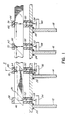
- a backplane 10 which may be a printed circuit board or other planar member, has a plurality of circuit cards 12, 14, 16 and 18 mounted on its one face so as to extend perpendicular to the backplane 10.
- the circuit cards 12, 14, 16 and 18 are coupled to the backplane by electrical connectors 20, 22, 24, and 26, respectively, adjacent holes 28, 30, 32 and 34, respectively, which extend through the backplane 10.
- An optical conductor 36 is mounted on the opposite face of the backplane 10 by a set of seating members 38, 40, 42 and 44 spaced apart along its length, one over each of holes 28, 30, 32 and 34, respectively.
- each seating member 38, 40, 42 or 44 comprises a block of aluminum having a seating in the form of a square aperture 46 to receive and positively locate the optical conductor or waveguide 36.
- the optical conductor 36 has a polygonal, specifically square, cross-sectional shape and is a close fit in the aperture 46.
- the facets comprise planar surfaces, at least the lowermost one of which accurately locates the conductor 36 with its bottom facet parallel to the backplane 10.
- the base of each seating member 38, 40, 42, or 44 has an anchorage in the form of a set of spigots 48 (see Figure 2) which project beyond the end of the seating member to engage in corresponding holes 50 in the backplane 10.
- the spigot holes 50 surround the corresponding one of holes 28, 30, 32 and 34 so that each seating member is located over the corresponding one of holes 28, 30, 32 and 34.
- a hole or cavity 51 extends between the square aperture 46 and the anchorage end of the seating member 42.
- a lens 52 is supported to extend across the hole 51 between the base of square aperture 46 and the anchorage 48.
- Each lens 52 is arranged with its optical axis perpendicular to the longitudinal axis of the optical waveguide 36 and aligned, through the hole 28, 30, 32 or 34, with an optical element in the form of a receiver 54, 56 or 58 or an optical transmitter 60 mounted on the corresponding one of the circuit cards 12, 14, 16, and 18.
- the optical transmitters may be light-emitting diodes and the receivers photodiodes.
- Each LED or photodiode is fitted with a lens 53 corresponding to lens 52 (see Figure 1).
- lasers could be used.
- the LED, photodiode or laser need not be located immediately adjacent the backplane but could be positioned some distance away, possibly not even on the circuit card, and connected by means of another optical conductor or optical fiber, which then constitutes the transmitter or receiver.
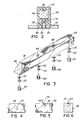
- the optical conductor 36 has a series of reflector means or taps formed by inclined planar surfaces 62, 64, 66 and 68 aligned with the lenses 52 in seating members 38, 40, 42 and 44, respectively.
- the inclined surfaces 62, 64 and 66 are formed as mitred ends of a series of circular cavities 70, 72 and 74, respectively (see Figure 5).
- the final inclined surface 62 is formed by mitring the end of the rod 36.
- Each cavity 70, 72 or 74 is conveniently formed during moulding of the optical waveguide 36 by means of a mould insert in the form of an obliquely truncated round rod which may readily be obtained with the required precision.
- the inclined reflector surfaces 62, 64, 66 and 68 may be coated with metal, for example gold or aluminum, to maximize their reflectance.
- the inclined surface 68 associated with the transmitter 60 is inclined oppositely to the other inclined surfaces so that light from the transmitter 60 is reflected through ninety degrees to travel along the optical waveguide 36 parallel to its longitudinal axis.
- At each of the "receiver" inclined surfaces 62, 64 and 66 a portion of the light is reflected, again through ninety degrees, to pass through the associated lens 52, the backplane 10, and the receiver's lens 53, to impinge upon the receiver 54, 56 or 58.
- the amount of light reflected will depend upon the area of the inclined surface relative to the cross-sectional area of the rod. Typically, this will be 2-4%.
- the inclined surfaces may be made to have a larger area the further they are away from the transmitter 60 in order to maximize the number of taps permitted. Masking or shadowing of one inclined surface by the preceding one has not been found to be a significant problem.
- the combination of small tap area, large inter-tap spacing, and multimode transmission serves to ensure that light by-passing one inclined reflector surface reaches the next.
- the optical conductor may be convenient for the optical conductor to receive a light signal from, say, an optical fiber which is behind the backplane 10.
- the embodiment of Figure 7 shows a convenient way of coupling such an optical fiber 80 to the optical conductor 36.
- the latter is similar to the optical conductor shown in Figures 3-6, in that it has a series of reflector surfaces 64, 66 etc. but differs in that the reflector surface 82 arranged to receive light from the optical fiber 80 is on the opposite side of the optical conductor 36, i.e. adjacent the backplane 36.
- the associated support member 84 has spigots 86 securing it to the backplane 36, and a lens 88 mounted in a hole 90 in the part of the support member 84, that is, on the side away from the backplane 36.
- the optical fiber 80 is terminated in a connector 92 which houses a second lens 94.
- the connector 92 fits over the end of the support member 84 so that the axes of the lenses 88 and 94 are substantially aligned.
- the light signal can be brought into the cabinet from the rear, i.e. behind the backplane, as is usual. It is fed into the optical conductor 36 via the connector 92, lenses 88, 94 and directed along the optical conductor 36 by the reflector surface 82.
- the other reflector surfaces 64, 66 etc. distribute the signal to the circuit cards as described with respect to Figure 1.
- optical conductors 100, 102, 104 and 106 extend parallel to each other on a backplane-mounted support (not shown).
- One transmitter and two receivers are mounted on each of four circuit cards 108, 110, 112 and 114, respectively.
- the transmitters and receivers are connected to optical conductors 102 and 104, respectively.
- Optical conductor 104 is shown coupled at one end (light can, of course, be launched into these optical conductors through the end) to a transmitter 116 and is coupled via its reflectors to first ones of the receiver ports of circuit cards 108, 110, 112 and 114.
- the other receiver ports are coupled laterally to the optical conductor 106, which is coupled at its end to a control/supervisory transmitter 118.
- optical conductor 102 is coupled by a U-bend (actually two 45 degree bends such as disclosed in Canadian patent application number 517,834), to the fourth optical conductor 100, which carries the data signals in the opposite direction to the data receiver 120.
- the inclined surface (68 or 82) which receives light from the transmitter may be larger than usual, for example the whole of the oblique cross-sectional area of the conductor.
- the rod may be of other polygonal shapes, such as hexagonal, triangular or octagonal, and the inclined reflector surfaces may be provided in the same surface as that from which the light emerges.
- the light source employs multimodal excitation, specifically with a range of angles of internal light rays of about 10 degrees.
- the spacing between aligned reflectors need not be particularly large to avoid shadowing of one reflector by the preceding reflector.
- the spacing between the adjacent reflectors was about 50 mm, giving a ratio of reflector spacing to reflector diameter of about 150:1.
- the reflector surfaces in the specific embodiment will reflect only about 2-4% of the light travelling along the conductor, if light is being transmitted into the waveguide via such surfaces, they will reflect substantially all of the light. This is mainly because the lens system enables one to image the source onto the reflector so that substantially all of the light gets transmitted along the conductor. The difference is that the transmitted light is still concentrated into a few modes, whereas the light in the waveguide comprises many more modes.
- the reflector means in the specific embodiment comprise planar surfaces
- other types of reflective surfaces might be employed, for example the prismatic reflector surface disclosed and claimed in Canadian application number 517,834, or other means employing total internal reflection.
- the specific embodiment comprises a so-called directional coupler inasmuch as the inclined surface at each tap point is inclined in one direction only. It is envisaged that a bidirectional coupler could be provided by forming two oppositely-inclined surfaces at each tapping point. Then one would reflect light to travel, or travelling in, one direction along the waveguide and the other would reflect light to travel, or travelling in, the opposite direction.
- oppositely-inclined surfaces might be spaced apart, perhaps to serve different circuit cards or different parts of the same card.
- circular cavities are preferred for ease of mould manufacture, other shapes are comprehended by the invention; in particular, square or otherwise rectangular cross-section might be preferred because such a tap has maximum efficiency due to minimum loss of light.
- the inclined surfaces may be provided in any combination of orientations to give 1:n distribution, n:1 concentration or multiplexing, or even n:m, i.e. plural transmitters to plural receivers.
Landscapes
- Physics & Mathematics (AREA)
- General Physics & Mathematics (AREA)
- Optics & Photonics (AREA)
- Optical Couplings Of Light Guides (AREA)
Priority Applications (1)
| Application Number | Priority Date | Filing Date | Title |
|---|---|---|---|
| AT87301676T ATE99809T1 (de) | 1986-03-12 | 1987-02-25 | Optische leiter. |
Applications Claiming Priority (4)
| Application Number | Priority Date | Filing Date | Title |
|---|---|---|---|
| CA 503968 CA1277164C (en) | 1986-03-12 | 1986-03-12 | Optical conductors |
| CA503968 | 1986-03-12 | ||
| US92875486A | 1986-11-10 | 1986-11-10 | |
| US928754 | 1986-11-10 |
Publications (3)
| Publication Number | Publication Date |
|---|---|
| EP0237236A2 true EP0237236A2 (de) | 1987-09-16 |
| EP0237236A3 EP0237236A3 (en) | 1989-11-08 |
| EP0237236B1 EP0237236B1 (de) | 1994-01-05 |
Family
ID=25670934
Family Applications (1)
| Application Number | Title | Priority Date | Filing Date |
|---|---|---|---|
| EP87301676A Expired - Lifetime EP0237236B1 (de) | 1986-03-12 | 1987-02-25 | Optische Leiter |
Country Status (2)
| Country | Link |
|---|---|
| EP (1) | EP0237236B1 (de) |
| DE (1) | DE3788664T2 (de) |
Cited By (4)
| Publication number | Priority date | Publication date | Assignee | Title |
|---|---|---|---|---|
| FR2723644A1 (fr) * | 1994-08-09 | 1996-02-16 | Matra Defense | Reseau d'interconnexion optique |
| EP0864894A1 (de) * | 1997-02-18 | 1998-09-16 | International Technology Consultants Ltd. | Ein Wellenleiter |
| DE10335036A1 (de) * | 2003-08-01 | 2005-03-03 | Siemens Ag | Modulares System |
| DE202017104593U1 (de) * | 2017-08-01 | 2018-11-06 | Wago Verwaltungsgesellschaft Mbh | Optische Kommunikationseinrichtung, Sockeleinheit und elektronische Einrichtung |
Family Cites Families (4)
| Publication number | Priority date | Publication date | Assignee | Title |
|---|---|---|---|---|
| CH599558A5 (de) * | 1976-03-16 | 1978-05-31 | Patelhold Patentverwertung | |
| DE2939456A1 (de) * | 1979-09-28 | 1981-04-16 | Siemens AG, 1000 Berlin und 8000 München | Verfahren zur herstellung von integrierten halbleiterschaltungen, insbesondere ccd-schaltungen, mit selbstjustierten, nichtueberlappenden poly-silizium-elektroden |
| US4447118A (en) * | 1981-09-21 | 1984-05-08 | The Boeing Company | Optical information transfer system |
| DE3400480A1 (de) * | 1984-01-09 | 1985-09-05 | Klaus-Rüdiger Dipl.-Ing. 4350 Recklinghausen Hase | Optisches bus-system (optobus) mit planarem lichtleiter fuer datenverarbeitende systeme, insbesondere mikrorechner |
-
1987
- 1987-02-25 DE DE19873788664 patent/DE3788664T2/de not_active Expired - Fee Related
- 1987-02-25 EP EP87301676A patent/EP0237236B1/de not_active Expired - Lifetime
Cited By (4)
| Publication number | Priority date | Publication date | Assignee | Title |
|---|---|---|---|---|
| FR2723644A1 (fr) * | 1994-08-09 | 1996-02-16 | Matra Defense | Reseau d'interconnexion optique |
| EP0864894A1 (de) * | 1997-02-18 | 1998-09-16 | International Technology Consultants Ltd. | Ein Wellenleiter |
| DE10335036A1 (de) * | 2003-08-01 | 2005-03-03 | Siemens Ag | Modulares System |
| DE202017104593U1 (de) * | 2017-08-01 | 2018-11-06 | Wago Verwaltungsgesellschaft Mbh | Optische Kommunikationseinrichtung, Sockeleinheit und elektronische Einrichtung |
Also Published As
| Publication number | Publication date |
|---|---|
| DE3788664D1 (de) | 1994-02-17 |
| EP0237236A3 (en) | 1989-11-08 |
| DE3788664T2 (de) | 1994-05-05 |
| EP0237236B1 (de) | 1994-01-05 |
Similar Documents
| Publication | Publication Date | Title |
|---|---|---|
| US4872739A (en) | Optical busbar | |
| US6422761B1 (en) | Angled optical connector | |
| US6973248B2 (en) | Planar optical component, and a coupling device for coupling light between a planar optical component and an optical assembly | |
| US10386589B2 (en) | Hybrid cable-to-board connector | |
| US4653845A (en) | Fiber optic star coupler | |
| KR101159049B1 (ko) | 광 파이버 전력 분할기 모듈 장치 | |
| US4744617A (en) | Mounting optical busbars on backplanes | |
| CN102472870B (zh) | 光学纤维互连装置 | |
| US6672939B2 (en) | Cost-effective side-coupling polymer fiber optics for optical interconnections | |
| EP0903601B1 (de) | Mehrkanaliges optisches Empfänger-/Sendersystem | |
| Moisel et al. | Optical backplanes with integrated polymer waveguides | |
| EP3807686A1 (de) | Optische steckverbinder und lösbare optische steckverbinderanordnungen für optische chips | |
| US6097864A (en) | Branching optical wave guide configuration | |
| KR20160135707A (ko) | 광결합 소자 및 광결합 유닛 | |
| US6931195B2 (en) | Parallel fiber-fan-out optical interconnect for fiber optic system | |
| US6408121B1 (en) | Optical communication module | |
| US6789953B1 (en) | Optical coupler | |
| CN119535695A (zh) | 一种基于穿透基底准直光栅的光芯片-光纤耦合器 | |
| US6512618B1 (en) | Broadcast optical communication system employing waveguide having grating normal to sources and detectors | |
| US7489841B2 (en) | Device for transferring optical signals by means of planar optical conductors | |
| EP0237236B1 (de) | Optische Leiter | |
| US6470114B1 (en) | Retroreflective conductors for optical fiber interconnects | |
| CA1277164C (en) | Optical conductors | |
| US4747653A (en) | Crossover arrangement for optical conductors | |
| CN219737829U (zh) | 一种光发射器件和光模块 |
Legal Events
| Date | Code | Title | Description |
|---|---|---|---|
| PUAI | Public reference made under article 153(3) epc to a published international application that has entered the european phase |
Free format text: ORIGINAL CODE: 0009012 |
|
| AK | Designated contracting states |
Kind code of ref document: A2 Designated state(s): AT DE FR GB NL SE |
|
| PUAL | Search report despatched |
Free format text: ORIGINAL CODE: 0009013 |
|
| AK | Designated contracting states |
Kind code of ref document: A3 Designated state(s): AT DE FR GB NL SE |
|
| RHK1 | Main classification (correction) |
Ipc: G02B 6/42 |
|
| 17P | Request for examination filed |
Effective date: 19900321 |
|
| 17Q | First examination report despatched |
Effective date: 19911104 |
|
| GRAA | (expected) grant |
Free format text: ORIGINAL CODE: 0009210 |
|
| AK | Designated contracting states |
Kind code of ref document: B1 Designated state(s): AT DE FR GB NL SE |
|
| PG25 | Lapsed in a contracting state [announced via postgrant information from national office to epo] |
Ref country code: SE Effective date: 19940105 Ref country code: NL Effective date: 19940105 Ref country code: AT Effective date: 19940105 |
|
| REF | Corresponds to: |
Ref document number: 99809 Country of ref document: AT Date of ref document: 19940115 Kind code of ref document: T |
|
| ET | Fr: translation filed | ||
| REF | Corresponds to: |
Ref document number: 3788664 Country of ref document: DE Date of ref document: 19940217 |
|
| NLV1 | Nl: lapsed or annulled due to failure to fulfill the requirements of art. 29p and 29m of the patents act | ||
| PLBE | No opposition filed within time limit |
Free format text: ORIGINAL CODE: 0009261 |
|
| STAA | Information on the status of an ep patent application or granted ep patent |
Free format text: STATUS: NO OPPOSITION FILED WITHIN TIME LIMIT |
|
| 26N | No opposition filed | ||
| PGFP | Annual fee paid to national office [announced via postgrant information from national office to epo] |
Ref country code: FR Payment date: 20010213 Year of fee payment: 15 |
|
| PGFP | Annual fee paid to national office [announced via postgrant information from national office to epo] |
Ref country code: GB Payment date: 20010221 Year of fee payment: 15 Ref country code: DE Payment date: 20010221 Year of fee payment: 15 |
|
| REG | Reference to a national code |
Ref country code: GB Ref legal event code: IF02 |
|
| PG25 | Lapsed in a contracting state [announced via postgrant information from national office to epo] |
Ref country code: GB Free format text: LAPSE BECAUSE OF NON-PAYMENT OF DUE FEES Effective date: 20020225 |
|
| PG25 | Lapsed in a contracting state [announced via postgrant information from national office to epo] |
Ref country code: DE Free format text: LAPSE BECAUSE OF NON-PAYMENT OF DUE FEES Effective date: 20020903 |
|
| GBPC | Gb: european patent ceased through non-payment of renewal fee |
Effective date: 20020225 |
|
| PG25 | Lapsed in a contracting state [announced via postgrant information from national office to epo] |
Ref country code: FR Free format text: LAPSE BECAUSE OF NON-PAYMENT OF DUE FEES Effective date: 20021031 |
|
| REG | Reference to a national code |
Ref country code: FR Ref legal event code: ST |