EP0237765A2 - Dispositif pour générer un signal de rotation - Google Patents
Dispositif pour générer un signal de rotation Download PDFInfo
- Publication number
- EP0237765A2 EP0237765A2 EP87101774A EP87101774A EP0237765A2 EP 0237765 A2 EP0237765 A2 EP 0237765A2 EP 87101774 A EP87101774 A EP 87101774A EP 87101774 A EP87101774 A EP 87101774A EP 0237765 A2 EP0237765 A2 EP 0237765A2
- Authority
- EP
- European Patent Office
- Prior art keywords
- signal
- output
- rotor
- signal generator
- delivers
- Prior art date
- Legal status (The legal status is an assumption and is not a legal conclusion. Google has not performed a legal analysis and makes no representation as to the accuracy of the status listed.)
- Granted
Links
- 230000000630 rising effect Effects 0.000 claims abstract description 6
- 238000010586 diagram Methods 0.000 description 10
- 239000003990 capacitor Substances 0.000 description 9
- 230000004069 differentiation Effects 0.000 description 5
- 230000004044 response Effects 0.000 description 3
- 239000013256 coordination polymer Substances 0.000 description 2
- 238000001514 detection method Methods 0.000 description 2
- 101150073536 FET3 gene Proteins 0.000 description 1
- 230000004075 alteration Effects 0.000 description 1
- 230000015556 catabolic process Effects 0.000 description 1
- 230000008859 change Effects 0.000 description 1
- 238000006731 degradation reaction Methods 0.000 description 1
- 230000005669 field effect Effects 0.000 description 1
- 230000004043 responsiveness Effects 0.000 description 1
- 229920006395 saturated elastomer Polymers 0.000 description 1
- 230000001360 synchronised effect Effects 0.000 description 1
- 230000001052 transient effect Effects 0.000 description 1
Images



Classifications
-
- G—PHYSICS
- G01—MEASURING; TESTING
- G01P—MEASURING LINEAR OR ANGULAR SPEED, ACCELERATION, DECELERATION, OR SHOCK; INDICATING PRESENCE, ABSENCE, OR DIRECTION, OF MOVEMENT
- G01P3/00—Measuring linear or angular speed; Measuring differences of linear or angular speeds
- G01P3/42—Devices characterised by the use of electric or magnetic means
- G01P3/44—Devices characterised by the use of electric or magnetic means for measuring angular speed
- G01P3/46—Devices characterised by the use of electric or magnetic means for measuring angular speed by measuring amplitude of generated current or voltage
Definitions
- the present invention relates to a rotating signal generator apparatus having a signal generator such as sine encoder for producing a signal whose frequency is proportional to the rotational speed of a rotor and whose rising and falling angles near points crossing zero become larger with the rotating speed of the rotor.
- the apparatus generates the rotating signal of the rotational speed, the rotational position or the like.
- an angle signal comparator for producing a first signal of amplitude corresponding to the rising and falling angles of the output of the signal generator as stated above, and a frequency comparator for producing a second signal of amplitude corresponding to the frequency of the output of the signal generator are provided to derive the rotating signal of the rotor by using the first signal in a low speed range and the second signal in a high speed range.
- the magnitude of the first signal exhibits a characteristic in which it is properly proportional to the rotational frequency of the rotor in the low speed range, but it becomes unproportional in the high speed range.
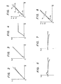
- the magnitude of the second signal is properly proportional in the high speed range but is unproportional in the low speed range as illustrated in Fig. 3.
- the present invention has been made in view of such drawbacks, and has for its object to provide a rotating signal generator apparatus which can generate a rotating signal of excellent characteristics without discontinuing its output signal over a range from a low speed range to a high speed range.
- the present invention consists in disposing a calculator and a corrector in addition to a signal generator, an angle signal comparator and a frequency signal comparator.
- the calculator calculates the difference between a first signal and a second signal, and the corrector corrects the first signal or the second signal with the output of the calculator.
- the first signal being the output of the angle signal comparator is properly proportional to the speed of the rotor in the low speed range, but the rate at which the signal increases relative to the increase of the rotational speed diminishes in the high speed range.
- the second signal being the output of the frequency signal comparator is properly proportional in the high speed range, but it exhibits only values smaller than on a proportionality line in the low speed range.
- the second signal becomes smaller than the first signal in the low speed range, and the second signal becomes larger than the first signal in the high speed range. Therefore, a point P at which the first signal and the second signal intersect arises as shown in Fig. 5.
- V 1 denote the first signal
- V 2 denote the second signal
- the signal V 1 left intact is delivered in a range of lower speeds with respect to the point P, and the component V 3 is corrected for the signal V 1 at higher speeds with respect to the point P, whereby the rotating signal of characteristic superior to the characteristic curve of V 1 or V 2 alone can be generated.
- the combined characteristic curve is obtained on the basis of the characteristic curve V 1 in both the higher speed range and the lower speed range with respect to the point P, the signal can be produced continuously.
- the signal V 2 left intact is delivered in the higher speed range with respect to the point P, and the component V 3 is corrected for the signal V 2 at the lower speeds with respect to the point P, whereby the rotating signal of characteristic superior to the characteristic curve of V 1 or V 2 alone can be generated.
- the combined characteristic curve is obtained on the basis of the characteristic curve V 2 in both the higher speed range and the lower speed range with respect to the point P, the signal can be produced continuously.
- the signals of a signal generator 100 which generates the "A" phase and "B" phase of sine waveform having almost equal amplitudes and having a phase difference of 90 0 therebetween, owing to the rotation of a rotor 110 as in an electric motor, are differentiated by an angle signal comparator 1.
- the differential waveforms of the "A" phase and the "B" phase near points crossing zero are switched to deliver a first signal V 1 which is plus for the positive direction rotation of the rotor and minus for the negative direction rotation.
- the "A" phase and the "B” phase have the sine waveforms converted into rectangular waves by a waveform shaper 2, whereupon a second signal V 2 which is a plus voltage for the positive direction rotation and a minus voltage for the negative direction rotation is delivered by an F/V (frequency/voltage) comparator 3. That is, a frequency signal comparator 101 is constructed of the waveform shaper 2 and the F/V comparator 3.
- the first signal V 1 has its linearity worsened by the degradations of the frequency characteristics of the "A" and "B” phases in a high speed range as illustrated in Fig. 2.
- the second signal V 2 has its pulse intervals lengthened at low speeds and therefore has its ripple increased, and it finally fails to be produced as illustrated by a characteristic in Fig. 3.
- both the first and second signals V and V 21 V 1 - V 2 is calculated by a calculator 4, and a signal 3 having a characteristic in Fig. 6 is delivered.
- a limiter signal generator 8 produces a limiter signal V 6 in Fig. 4 on the basis of the output V 2 of the F/V comparator 3, so that the output signal V 5 of the correct limiter 6 is limited to zero at the low speeds. Therefore, the characteristic in Fig. 6 changes as shown in Fig. 7.
- a corrector 102 is constructed of the correct limiter 6, the limiter signal generator 8 and the subtraction circuit 7. Since the signal V s is a minus voltage in Fig. 7, the subtraction circuit results in adding the absolute value V 5 to the voltage V 1 , and the velocity feedback signal of good linearity is obtained as shown at V f in Fig.
- the output of the calculator 4 is limited to zero by the correct limiter 6, and hence, the velocity feedback signal based on the gradient differential system is generated.
- Fig. 9 shows an embodiment in which the signal of the limiter signal generator 8 in Fig. 1 is detected from the output signal V 1 of the angle signal comparator 1, and the operation of which is basically the same as in Fig. 1.
- Fig. 10(a) is a diagram in the case where the actual rotational frequency N of the rotor 110 has abruptly risen from a medium speed to a high speed.
- the first signal V 1 responds immediately as shown in Fig. 10(b), but the second signal V 2 undergoes a considerable delay as shown in the same figure.
- the second signal V 2 based on the F/V system affords a preciser value rather than the first signal V 1 .
- the output V 3 of the calculator 4 becomes as shown in Fig. 10(c), and it is changed as shown at V 4 in Fig. 10(c) by the first order lag circuit 5.
- numerals 111 and 112 indicate NOT circuits
- numeral 113 a first switch control signal generator
- numeral 114 a second switch control signal generator
- numeral 115 "A” phase analog switches
- numeral 116 "B” phase analog switches numerals 117 and 118 differentiation circuits
- numeral 119 slit removing analog switches
- numeral 120 a NOT amplifier circuit
- numeral 121 a NOT amplifier circuit for adjusting a sign.
- the "A" phase signal A and the inverted “A” phase signal A are received through the analog switches 115, and the parts of the signals A and A having the same gradient are taken out.
- the output of the analog switches 115 becomes an "A" phase gradient signal AA shown in Fig. 12.
- the gradient signals AA and BB of the "A" and “B" phases are differentiated by the respective differentiation circuits 117 and 118 each being constructed of a capacitor and a resistor.
- the outputs of the respective differentiation circuits 117 and 118 are differential signals dAA and dBB shown in Fig. 12.
- These signals dAA and dBB are formed with slits as illustrated. In order to eliminate the slits, therefore, only parts of 90 ° near the peaks of the respective differential signals dBB and dAA are derived through the slit removing analog switches 119 and are combined.
- the combined signal is amplified by the NOT circuit 120, to obtain a speed detection signal E.
- the NOT circuit 121 serves to deliver the first signal V 1 which is the plus output for the positive direction rotation and the minus output for the negative direction rotation.
- the control of the "A" phase analog switches 115 is performed with the output signals SF and SF of the first switch control signal generator 113. These output signals SF and SF are produced by comparing the "B" phase signal B and the inverted "B" phase signal B.
- control of the "B" phase analog switches 116 is performed with the output signals SE and SE of the first switch control signal generator 113. These output signals SE and SE are produced by comparing the "A" phase signal A and the inverted "A” phase signal A.
- the slit removing analog switches 119 for eliminating the slits are controlled with the output signals SG and SG of the second switch control signal generator 114.
- the signal SG is obtained by comparing the "A" phase signal A with the "B” phase signal B and also comparing the "A" phase signal A with the inverted “B” phase signal B and then taking the exclusive OR of the comparison outputs.
- Fig. 13 shows the practicable embodiment of the waveform shaper 2 as well as the F/V comparator 3 in Fig. 1. It is as stated before that the frequency signal comparator 101 is constructed of the waveform shaper 2 and the F/V comparator 3.
- the "A" phase and "B” phase of sine waveform with the phase difference of 90 ° as produced from the signal generator 100 are respectively passed through filters R 1 , C 1 and R 2 , C 2 , whereupon the passed signals are converted into the rectangular waves having the phase difference of 90 ° by means of hysteresis comparators CP1, CP 2 and resistors R 3 - R 8 .
- the rectangular waves are passed through an exclusive OR gate IC 2 to double the pulse frequency, and the resulting signal is applied to an F/V converter IC 1 .
- This F/V converter detects the falls of the input pulses when the pulses exceed an input threshold voltage of -0.6 V, and it supplies a pin 13 with a voltage proportional to an input frequency.
- a capacitor C 3 and resistors R 9 , R 10 configure a differentiation circuit so as to pass the input pulses through the threshold voltage of -0.6 V.
- the gain of the F/V converter IC 1 is determined by a resistor R 11 , and the filter time constant thereof by the resistor R 11 and a capacitor C 5 . Therefore, the capacitance of the capacitor C 5 is enlarged for reducing the ripple of the output. This measure, however, worsens the responsiveness.
- a capacitor C 4 determines the pulse width of a one-shot multivibrator which produces a pulse of the fixed width synchronous with the fall input of the F/V converter.
- the output of the F/V converter is delivered as an absolute value in the plus sign. Therefore, analog switches employing field effect transistors FET 1 - FET3, and resistors R 20 - R 23 are disposed on the input side of an operational amplifier OP 1 , whereupon for the positive direction rotation, the amplifier OP 1 is operated as an inverting amplifier by turning “on” the transistor FET 1 and “off” the transistors FET 2 and FET 3 , and for the negative direction rotation, the amplifier OP 1 is operated as a non-inverting amplifier by turning “off” the transistor FET 1 and “on” the transistors FET 2 and FET 3 .
- the F/V comparator 3 with the polarity which renders the output V 2 a minus voltage for the positive direction rotation and a plus voltage for the negative direction rotation is constructed.
- a zero- crossing comparator CP 3 detects the rotating direction from the first signal V 1 which is the output of the angle signal comparator 1 based on the gradient differentiation.
- the detected signal has its level changed by resistors R 12 , R 13 , a diode D 1 and a transistor Q 1 , and the resulting signal is applied to an inverter gate IC 3 and then to an inverter gate IC 4 so as to operate the switches FET 1 - FET 3 . - FET 3 .
- the second signal V 2 being the output of the F/V comparator 3 has its difference voltage from the first signal V 1 being the output of the angle signal comparator 1 detected by an amplifier OP 51 and resistors R 51 - R 54 which constitute the calculator 4 shown in Fig. 14.
- a capacitor CT indicated by a broken line between the output of the amplifier OP 51 and the minus input terminal thereof functions as the first order lag circuit shown in Fig. 1. The first order lag is not formed when the capacitor CT is detached, and the first order lag circuit is established by adding the capacitor CT.
- the limiter signal generator 8 is configured as a circuit which receives this output signal V 21 at the pin 13 and which affords a dead band near the zero input as shown in Fig. 15 by means of an amplifier OP 52 , resistors R 55 - R 58 and diodes D53 , D 54 .
- a value V 21x can be adjusted by a variable resistor VR 51 in Fig. 14, and it determines the point of time at which the correction of the first signal V 1 with the output of the calculator 4 is started.
- the variable resistor may well be replaced with resistors for voltage division. The reason why the output V 6 remains unchanged when the input V 21 in Fig. 15 is great, is that the amplifier OP52 is saturated. This signal V 6 limits the output of the difference voltage detector 4 in the correct limiter 6.
- the signal V 6 provides a signal V61 to serve as the minus side limiter signal of the output voltage V 3 of the amplifier OP 51 and a signal V 62 to serve as the plus side limiter signal thereof by means of NOT amplifier circuits 0P 53 , OP 54 and resistors R 59 - R 64 .
- Resistors R 65 - R 68 for dividing the limiter signals and the output signal V 3 of the calculator 4, and diodes D 51 , D 52 are connected.
- an incomplete limiter circuit is constructed.
- the divided voltage of the node of the resistors R 65 and R 66 between the signal V 3 and the signal V 61 changes gradually from a plus voltage toward zero.
- the diode D 51 turns "on,” and current having flowed through the resistor R 54 of the amplifier OP 51 till then flows to the diode D 51 . Therefore, the output V 3 can no longer rise, and the limiter operation is effected.
- the limiter circuit configured of the elements D 51 , D 52 and R 65 - R 68 is not a complete limiter circuit, but its output rises slightly beyond the limit point.
- a limiter correction circuit is constructed of amplifiers 0P 55 , OP 56 , resistors R 69 - R 76 and diodes D 55 - D 58 . That is, the limiter correction circuit is a circuit for canceling out the component having risen beyond the limit point on account of the signals V 61 and V 3 and the component having risen beyond the limit point on account of the signals V 62 and V 3 .
- the signal V 5 in Fig. 1 is indicated by a sum V 3 + V63 + V 64 in Fig. 14.
- the first signal V being the output of the angle signal comparator 1 is subtracted by elements OP 57 and R 77 - R 82 through a resistor R 80 , whereupon the output V f is delivered.
- the present invention is not restricted to the foregoing embodiments, but various alterations are possible.
- a device which generates a signal in a single phase can be used as the signal generator.
- a device which generates signals in three phases can, of course, be used.
- the detection of the rotating direction is naturally easy.
- the case employing the limiter 6 has been explained.
- unidirectional conduction means 140 is connected as indicated by broken lines in Fig.
- the first signal V 1 left intact is delivered as the output V f in the low speed range in which the signal V 3 is plus, and the first signal V 1 is corrected with the signal V 3 in the high speed range in which the signal V 3 is minus, namely, in the range in which the first signal V 1 becomes unproportional to the rotational frequency.
Landscapes
- Physics & Mathematics (AREA)
- General Physics & Mathematics (AREA)
- Transmission And Conversion Of Sensor Element Output (AREA)
- Control Of Eletrric Generators (AREA)
- Control Of Motors That Do Not Use Commutators (AREA)
Applications Claiming Priority (2)
| Application Number | Priority Date | Filing Date | Title |
|---|---|---|---|
| JP61032931A JPH0750116B2 (ja) | 1986-02-19 | 1986-02-19 | 回転情報出力装置 |
| JP32931/86 | 1986-02-19 |
Publications (3)
| Publication Number | Publication Date |
|---|---|
| EP0237765A2 true EP0237765A2 (fr) | 1987-09-23 |
| EP0237765A3 EP0237765A3 (en) | 1989-07-19 |
| EP0237765B1 EP0237765B1 (fr) | 1991-09-11 |
Family
ID=12372667
Family Applications (1)
| Application Number | Title | Priority Date | Filing Date |
|---|---|---|---|
| EP87101774A Expired EP0237765B1 (fr) | 1986-02-19 | 1987-02-09 | Dispositif pour générer un signal de rotation |
Country Status (4)
| Country | Link |
|---|---|
| US (1) | US4808933A (fr) |
| EP (1) | EP0237765B1 (fr) |
| JP (1) | JPH0750116B2 (fr) |
| DE (1) | DE3772801D1 (fr) |
Families Citing this family (7)
| Publication number | Priority date | Publication date | Assignee | Title |
|---|---|---|---|---|
| JPS6459805A (en) * | 1987-08-31 | 1989-03-07 | Taro Hino | Capacitor |
| JP2574873B2 (ja) * | 1988-08-24 | 1997-01-22 | 株式会社日立製作所 | 位置あるいは速度検出装置 |
| US5345171A (en) * | 1993-01-11 | 1994-09-06 | Caterpillar Inc. | Apparatus including a selectively connectable isolation transformer for determining the speed and direction of a rotating object |
| DE59306743D1 (de) * | 1993-03-08 | 1997-07-17 | Landis & Gyr Tech Innovat | Elektrische Überwachungsanordnung |
| GB9412774D0 (en) * | 1994-06-24 | 1994-08-17 | Genrad Ltd | Apparatus and method for testing |
| US6849811B1 (en) | 2000-07-31 | 2005-02-01 | General Electric Company | Methods and apparatus for transfer switch |
| US7375509B2 (en) * | 2005-03-02 | 2008-05-20 | Stoneridge Control Devices, Inc. | System and method for position sensing using inflection point position sensing of a sensor output |
Family Cites Families (5)
| Publication number | Priority date | Publication date | Assignee | Title |
|---|---|---|---|---|
| DE2324824C2 (de) * | 1973-05-16 | 1974-10-17 | Siemens Ag, 1000 Berlin Und 8000 Muenchen | Schaltungsanordnung zur Korrektur der Meßspannung eines analogen Drehzahlgebers |
| US3934200A (en) * | 1975-01-31 | 1976-01-20 | Landis Tool Company | Tachometer circuit |
| US4246536A (en) * | 1978-09-29 | 1981-01-20 | International Business Machines Corporation | Electronic velocity measurement device |
| JPS57175259A (en) * | 1981-04-22 | 1982-10-28 | Fanuc Ltd | Speed detector |
| US4575677A (en) * | 1984-05-25 | 1986-03-11 | Mobil Oil Corporation | Motor speed detector |
-
1986
- 1986-02-19 JP JP61032931A patent/JPH0750116B2/ja not_active Expired - Lifetime
-
1987
- 1987-02-09 DE DE8787101774T patent/DE3772801D1/de not_active Expired - Lifetime
- 1987-02-09 EP EP87101774A patent/EP0237765B1/fr not_active Expired
- 1987-02-11 US US07/013,545 patent/US4808933A/en not_active Expired - Fee Related
Also Published As
| Publication number | Publication date |
|---|---|
| JPH0750116B2 (ja) | 1995-05-31 |
| DE3772801D1 (de) | 1991-10-17 |
| EP0237765A3 (en) | 1989-07-19 |
| EP0237765B1 (fr) | 1991-09-11 |
| US4808933A (en) | 1989-02-28 |
| JPS62191768A (ja) | 1987-08-22 |
Similar Documents
| Publication | Publication Date | Title |
|---|---|---|
| KR910006700A (ko) | 회전축의 회전검출장치와 이 검출장치를 사용한 회전제어장치 | |
| US4298948A (en) | Method and apparatus for generating a digital representation of the instantaneous angular position of a rotating body and for generating rectangular coordinate equivalents thereof | |
| US4166247A (en) | Control systems for pulse width control type inverter | |
| EP0237765A2 (fr) | Dispositif pour générer un signal de rotation | |
| KR900002510B1 (ko) | 속도 검출장치 | |
| US5031087A (en) | Procedure for the selection of a bridge or bridge section in a rectifier bridge unit, and a bridge selector unit designed for implementing the procedure | |
| US3604995A (en) | Generator for producing a width-modulated square voltage | |
| US3760248A (en) | Induction motor control system with voltage controlled oscillator circuit | |
| RU2014701C1 (ru) | Измерительный орган направления мощности | |
| JPS62144021A (ja) | レゾルバ検出装置 | |
| JPH0457966B2 (fr) | ||
| KR910009090B1 (ko) | 디지탈방식의 리졸버/디지탈변환장치 | |
| US5289366A (en) | Method and apparatus for correction of a detected faulty actual valve of a signal affected by harmonic vibrations | |
| JPS63228992A (ja) | インバ−タ制御装置 | |
| SU1591120A1 (ru) | Peлe пepemehhoгo toka | |
| SU1148080A1 (ru) | Устройство дл управлени мостовым инвертором | |
| JPS6248476B2 (fr) | ||
| SU999014A1 (ru) | След ща система | |
| JPH0550236B2 (fr) | ||
| RU2199752C2 (ru) | Устройство для измерения скорости вращения | |
| EP0670474B1 (fr) | Système de controle pour dispositif électrique d'assistance de direction de véhicules et pour dispositif d'entrainement de moteurs pour machines d'usinage. | |
| KR0136411B1 (ko) | 고정밀 슬루 레이트를 가지는 위상추적 제어시스템 | |
| SU826547A1 (ru) | Способ одноканального асинхронного управления вентильным преобразователем 1 | |
| JPH02265315A (ja) | 波形整形方法及びその装置 | |
| SU1026056A1 (ru) | Устройство дл измерени скорости вращени |
Legal Events
| Date | Code | Title | Description |
|---|---|---|---|
| PUAI | Public reference made under article 153(3) epc to a published international application that has entered the european phase |
Free format text: ORIGINAL CODE: 0009012 |
|
| AK | Designated contracting states |
Kind code of ref document: A2 Designated state(s): DE FR GB |
|
| PUAL | Search report despatched |
Free format text: ORIGINAL CODE: 0009013 |
|
| AK | Designated contracting states |
Kind code of ref document: A3 Designated state(s): DE FR GB |
|
| 17P | Request for examination filed |
Effective date: 19890801 |
|
| 17Q | First examination report despatched |
Effective date: 19901212 |
|
| GRAA | (expected) grant |
Free format text: ORIGINAL CODE: 0009210 |
|
| AK | Designated contracting states |
Kind code of ref document: B1 Designated state(s): DE FR GB |
|
| REF | Corresponds to: |
Ref document number: 3772801 Country of ref document: DE Date of ref document: 19911017 |
|
| ET | Fr: translation filed | ||
| PLBE | No opposition filed within time limit |
Free format text: ORIGINAL CODE: 0009261 |
|
| STAA | Information on the status of an ep patent application or granted ep patent |
Free format text: STATUS: NO OPPOSITION FILED WITHIN TIME LIMIT |
|
| 26N | No opposition filed | ||
| PGFP | Annual fee paid to national office [announced via postgrant information from national office to epo] |
Ref country code: DE Payment date: 19960426 Year of fee payment: 10 |
|
| PGFP | Annual fee paid to national office [announced via postgrant information from national office to epo] |
Ref country code: GB Payment date: 19970130 Year of fee payment: 11 |
|
| PGFP | Annual fee paid to national office [announced via postgrant information from national office to epo] |
Ref country code: FR Payment date: 19970217 Year of fee payment: 11 |
|
| PG25 | Lapsed in a contracting state [announced via postgrant information from national office to epo] |
Ref country code: DE Effective date: 19971101 |
|
| PG25 | Lapsed in a contracting state [announced via postgrant information from national office to epo] |
Ref country code: GB Free format text: LAPSE BECAUSE OF NON-PAYMENT OF DUE FEES Effective date: 19980209 |
|
| PG25 | Lapsed in a contracting state [announced via postgrant information from national office to epo] |
Ref country code: FR Free format text: THE PATENT HAS BEEN ANNULLED BY A DECISION OF A NATIONAL AUTHORITY Effective date: 19980228 |
|
| GBPC | Gb: european patent ceased through non-payment of renewal fee |
Effective date: 19980209 |
|
| REG | Reference to a national code |
Ref country code: FR Ref legal event code: ST |