EP0238192A2 - Testeurs de circuits - Google Patents
Testeurs de circuits Download PDFInfo
- Publication number
- EP0238192A2 EP0238192A2 EP19870301196 EP87301196A EP0238192A2 EP 0238192 A2 EP0238192 A2 EP 0238192A2 EP 19870301196 EP19870301196 EP 19870301196 EP 87301196 A EP87301196 A EP 87301196A EP 0238192 A2 EP0238192 A2 EP 0238192A2
- Authority
- EP
- European Patent Office
- Prior art keywords
- test
- overdriving
- temperature
- circuit tester
- circuit
- Prior art date
- Legal status (The legal status is an assumption and is not a legal conclusion. Google has not performed a legal analysis and makes no representation as to the accuracy of the status listed.)
- Granted
Links
Images


Classifications
-
- G—PHYSICS
- G06—COMPUTING OR CALCULATING; COUNTING
- G06F—ELECTRIC DIGITAL DATA PROCESSING
- G06F11/00—Error detection; Error correction; Monitoring
- G06F11/22—Detection or location of defective computer hardware by testing during standby operation or during idle time, e.g. start-up testing
- G06F11/2273—Test methods
-
- G—PHYSICS
- G01—MEASURING; TESTING
- G01R—MEASURING ELECTRIC VARIABLES; MEASURING MAGNETIC VARIABLES
- G01R31/00—Arrangements for testing electric properties; Arrangements for locating electric faults; Arrangements for electrical testing characterised by what is being tested not provided for elsewhere
- G01R31/28—Testing of electronic circuits, e.g. by signal tracer
- G01R31/317—Testing of digital circuits
- G01R31/3181—Functional testing
- G01R31/319—Tester hardware, i.e. output processing circuits
- G01R31/31903—Tester hardware, i.e. output processing circuits tester configuration
- G01R31/31915—In-circuit Testers
Definitions
- the present invention relates to circuit testers, and in particular to circuit testers for performing a device level in-circuit test on a digital device.
- heating models have been developed which are a function of overdriving current and time. Since current can be estimated and the test duration is known, the temperature rise of overdriven devices may be estimated. An absolute maximum allowable device temperature is specified by the device manufacturer. so using the estimated temperature rise, a maximum allowable initial device temperature may be specified.
- variable delay interval not as a function of the test as performed, but as a function of the device, and the time it will require to cool to the maximum initial start temperature for the test.
- This approach leads to the insertion of a delay interval before each test.
- an assumption must be made. The only assumption that may be safely made is that the device has to cool from its maximum allowable temperature before each test.
- This regime although in most cases reducing the overall time required for a unconditionally safe device test pattern to be performed still has a number of problems. Clearly in most cases the device will not reach its maximum allowable temperature as a result of a previous ' test, and a waiting interval longer than necessary will consequently be specified.
- a particularly serious drawback of this regime is that a cool down waiting interval will be enforced before a test even if the overdriven device is already below the maximum initial start temperature for that test, when infact no delay is required at all.
- Present day ATE is configured to operate in two basic modes, a test specification mode, and a test performance mode.
- ATE In the test specification mode, ATE is loaded with circuit topography and device locations.Next the test patterns to test each individual device must be specified. Normally, these are held in ATE data files and are available as library routines to be inserted into the test specification en bloc. Occasionally, devices not in the library will be encountered, but normally an ATE mode which allows a component test pattern to be established for an unknown device may be entered. Once established, it is as though the test pattern had come from the library of which it may now form part.
- the ATE is also programmed to assess or invite an operator to assess the need for the placement of guard signals, that is signals applied purely to prevent unwanted component interactions.
- test performance mode may be entered for multiple repetition on boards to be tested.
- a further mode is available, which allows some analysis to be performed on the specified test to locate potentially damaging tests, which essentially involves identifying tests wherein outputs are overdriven and enforcing either duty-cycle or pre-test delay as described above.
- a circuit tester for testing board mounted components includes:
- the present invention represents a fundamental departure from prior art ATE since its configuration permits both use of board specific data during test specification or testing itself and the use of test interaction in the establishment of the cooling interval, by means of a parameter list for each test.
- a first parameter is measurment derived from either a previously tested or known to be good board or a historical derivation from such boards, or preferably from the actual board under test.
- This allows cooling intervals to be specificed for the configured devices and shows considerable improvement in the shortening of cooling intervals compared with prior art ATE in which intervals must be based on worst case values for isolated devices.
- the actual duration of a cooling interval will not be precisely specified in advance of a test, but will be dependent upon the actual tests performed as testing proceeds.
- a preferred implementation of this feature is to specify several cooling intervals a different one of which may be selected in the event of measurement of a short test, a normal test, a long test or a maximum duration test.
- a parameter may be the actual overdriving voltage used in a test, which may itself be selected based on previous measurements.
- a measured parameter may be overdriving current measured on the actual or a typical circuit board.
- the D-type flip-flops of device 10 each have a Clock Input ( A , CB ) a Data Input (D A . D B ) and a latched output (Q A . Q B ) . Additionally the flip-flops are provided with a Set Input (PRE A ,PRE B ) allowing the respective Data Output to be set high, and a Reset Input (CLR A . CLR B ) allowing the Data Output to be reset low.
- PRE A ,PRE B Set Input
- CLR A . CLR B Reset Input
- the truth table for each device is:- where X indicates an indeterminate state for a directly applied input.
- Each NAND gate (G A , G B ) of device 11 has two inputs (I 1A' I 2A ) (I 1B' I 2B ) and an output (A,B) as well as power supply corrections (not shown).
- the input/output truth table for each gate is:-
- the outputs (A, B) of the NAND device may be specified as:- and and for which the truth table is:- and of which the right hand three columns represents the operation of NAND gate G B of device 11.
- Curve 20 ( Figure 2) plots the temperature of device 11 when output A is overdriven between Temperature axis T (21) as ordinate and time axis ⁇ (22) as absicca.
- the device is heated from an initial or ambient temperature T amb for the duration of the overdriving test ⁇ test to reach a temperature T test (22).
- T test Taking a worst case example, the next test specified is found to also overdrive output A of device 11, and requires a duration ⁇ test next ⁇ Since the heating profile of the device is known by virtue of a heating model, a temperature T next may be specified, which is the highest temperature at which the next test may be commenced without the temperature exceeding T max the absolute maximum allowable temperature of device 11.
- a period ⁇ cool may be computed, which is the period required for the device to cool to T next The next test, if performed directly afterwards, would cause the device 11 to reach its absolute maximum value 23 after the test period ⁇ test next
- ⁇ max represents the maximum period for which a test can be run without exceeding device absolute maximum temperature. It is the practice in ATE for this time to be assessed and arrangements made for the test to be aborted before the period is exceeded, for example by means of an interupt _ timer loaded with a count representing ⁇ max which is counted down during the test to interupt the test on overflow. Were device 11 to reach T max then a period ⁇ cool max would be required for cooling before a subsequent test could be performed.
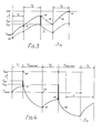
- a curve 30 ( Figure 3) shows a typical plot of temperature against time for three consecutive overdriving test perfomed by ATE configured in accordance with the present invention.
- the device reaches a temperture 31, from a starting temperature T start.
- ATE a test parameter list is maintained for the test which includes a measured parameter of test duration ⁇ 1 obtained from a previously tested board. Also included is the final temperature attained 31 and the maximum temperature at which the next test may be commenced T n2 .
- the second test may be commenced immediately, and the device heats to a temperature 32 at the end of this test, which lasts for a period ⁇ 2 .
- the test parameter list for this test includes measured period ⁇ 2 as well as the maximum safe test temperature for the third test T n3 . Since attained temperature 32 is above T n3 cooling is required and a delay of interval ⁇ cool 2' computed in accordance with a device cooling model, enforced to allow cooling to T n3 before the test is commenced. After the third test, which lasts for a period ⁇ 3 . the device reaches its absolute maximum at 33.
- the device Before the second test is performed, the device is allowed to cool during a period ⁇ coolmax to a termp a t ure 42.
- This cooling period ⁇ coolmax ) coolmax is that which would have been sufficient to cool the device from its absolute maximum temperature 43 to a safe starting temperature 44.
- the second test proceeds during an interval z 2 to raise the temperature of the device to a temperatuce 45.
- third test can proceed, a cooling delay of ⁇ coolmax is enforced. From the resulting curve 40 it will be noted that the test device is cooled unnecessarily.
- the improvement is made possible by the specification of a temperature parameter for each test, enabling optimized cooling delays to be enforced.
- the temperature parameters may be derived by exercising a device heating model in test specification, or preferably on-line during the test so that a value is available for the current value of device temperature, which may be transferred to or maintained as the test parameter list value.
- the enforced cooling delay is based - upon a representative device temperature attained at the end of a test, rather than a default or percentage (mark-space) delay as in prior art ATE.
- the device temperature may only be accurately computed if the actual start temperature is known. Where an actual ambient temperature measurement cannot be made, an assumed ambient may be used. For example prior to the first test only, a maximum cooling-interval ( ⁇ coolmax ) sufficient to cool the device device
- a cooling delay derived from another board will be adequate, since no significant variation is to be expected between boards.
- devices having a varying settling time for example a non-presettable counter which must be clocked to zero before testing, are in a circuit to be tested, preferably parameters are based on measurement made on that actual board under test.
- a test for gate B of device 11
- the test step is passed when the expected B output is measured by measurement nail 19 ( Figure 1), or when a transistion to the expected level occurs (as in tests 3 and 4). Since the D type flip-flop device is slow to clear, CLEARED tests 3 and 4 overrun the expected time. Test 3 should present no problem, but Test 4 is an overdriving test, which may be problematic, since this test is followed by another overdriving test, as already described.
- the actual running time of the test 20 us, is entered as a test parameter and used in a heating model to provide an attained device temperature. Subsequently a cooling model is exercised to enforce a cooling delay from this attained temperature to the safe temperature for commencement of the next test.
- ATE In ATE it is often preferred to do as little computation as possible during an actual test, transferring as much of the workload as possible to an off-line computation during the test specification phase.
- the present invention may be applied in this way by for example computing cooling delays to be enforced if particular test run times are encountered in practice. Then all that is required on line is a run time measurement, comparison, and interval selection.
- a predicted duration is stored as a test parameter. This duration may be computed, measured on a representative board or derived by averaging the durations of actual tests performed on several boards. Based on this predicted duration, a heating model is exercised to determine an attained temperature, and a cooling model exercised to determine the cooling delay required before a next overdriving test may be safely commenced. This predicted cooling delay is stored in machine memory. Additionally computed is the cooling time from absolute maximum allowable device temperature. T coolmax *
- test time is interrogated. If the actual test time is less than or equal to predicted test time, then the predicted cooling delay is enforced before the next overdriving test. Should however actual test duration exceed the predicted duration, ⁇ coolmax is enforced.
- a first test causes a temperature rise to a temperature 51. Since the attained temperature is above the safe start temperature for a next test ⁇ n2 , a cooling delay is required. Associated with the test is a predicted test duration ⁇ lp* Since the actual test duration ⁇ 1 , is less than predicted, a cooling delay ⁇ cool p is inserted before the next test. The period ⁇ cool p is sufficient for the device to cool from a temperature 52 to T n2 , the temperature at which the second test may be safely commenced. It will be appreciated that the actual device under test will infact cool to a temperature 53, below T n2 .
- a second test is initiated, which causes heating to a temperature 54 during a test interval ⁇ 2 . Since ⁇ 2 exceeds predicted interval T2 p for the second test a cooling delay ⁇ coolmax is enforced, sufficient to cool from device absolute maximum temperature to a temperature Tn3' that at which a third test may be safely commenced. In fact, since the device was not at its absolute maximum allowable temperature after the second test, a lower temperature 55 will be reached.
- the heating effect increases with overdriving voltage.
- the overdriving voltage may be an actual value measured during a test or a value specified in a test definition. Since the invention provides means for optimising cooling delay based upon actual overdriving voltage, the applied voltage itself may be selected to suit a particular test, allowing reduced applied voltage (and hence less device heating stess) compared with prior art ATE.
- the test parameter list carries an overdriving voltage to be used for each test, together with a corresponding cooling delay.
- the test schedule is inspected for an overdriving test, and with a known to be good circuit board in the fixture, a confirmation test performed of an overdriving test with full overdriving voltage applied.
- the test is then repeated with applied overdriving voltage reduced by 10% . If the test is still passed the test is repeated again with a 10% reduction in overdriving voltage, and so on until failure occurs, whereupon the lowest value of overdriving voltage giving a successful test is entered in the test parameter list as the overdriving voltage to! be used when that test is performed on actual production circuit boards. It will be appreciated that the overdriving stress applied during the test is thereby reduced compared with the same test with the full overdriving voltage applied.
- the specified reduced value of overdriving is used when the heating model is exercised to define the interval required.
- the invention provides not only lower overdriving stress, but also a reduced overall test time.
- ATE in accordance with the present invention reduced overdriving voltages and where appropriate cooling delay are held as parameters for each test. In operation the majority of boards may be successfully tested with the reduced values. However, there may be a minority of in specification boards which fail the reduced voltage test. ATE may be programmed in the test definition to repeat overdriving tests at full overdriving voltage in the event of a failure.
- a full length cooling interval is required, and so for each test the cooling delay corresponding to application of the full overdriving voltage is held as an additional test parameter for use in the event of a repeated test.
- a plurality of cooling invervals corresponding to various overdriving voltages may be stored as test parameteres.
- the overdriving voltage used for any particular test may be regarded as a current best estimate, and a histogram of previous test results used to improve the estimate.
- an algorithim which rapidly homes to the lowest applied voltage giving a successful test in most cases is preferred so that both undue device stress and undue test repeats are avoided.
- corresponding cooling intervals where required may be computed during testing, or a suitable interval value selected from a parameter look up table defined in the test specification phase, but exercising the heating model for various values.
- overdriving current Another parameter which may be measured to influence the selection of optimized cooling intervals is overdriving current.
- the actual current injected or sunk may be measured, alternatively a representative measurement may be obtained from a known to be good board during test definition, or an average of such measurements for an integrated circuit in which several devices are overdriven simulataneously, the sum of the individual device overdriving currents will sum in a power supply bond wire.
- bond wire heating is a potential cause of failure and a bond wire heating model may be exercised to establish safe cooling delays for various possible currents. Unfortunately since current flowing to or from the power supply rails for an individual device cannot be measured, an optimum cooling interval cannot be selected.
- the overdriving currents of indiviual devices are separately measured. and a summed value used in computations. Again, these values may be measured for the actual board under test and an appropriate interval selected from previous computed values. The individual values may be obtained by virtue of other overdriving tests where packaged devices are exercised alone. or a special overdriving measurement test may be inserted in the test schedule.
Landscapes
- Engineering & Computer Science (AREA)
- General Engineering & Computer Science (AREA)
- Theoretical Computer Science (AREA)
- General Physics & Mathematics (AREA)
- Physics & Mathematics (AREA)
- Computer Hardware Design (AREA)
- Quality & Reliability (AREA)
- Tests Of Electronic Circuits (AREA)
- Oscillators With Electromechanical Resonators (AREA)
- Steroid Compounds (AREA)
- Eye Examination Apparatus (AREA)
- Pens And Brushes (AREA)
- Chemical And Physical Treatments For Wood And The Like (AREA)
Priority Applications (1)
| Application Number | Priority Date | Filing Date | Title |
|---|---|---|---|
| AT87301196T ATE97238T1 (de) | 1986-02-14 | 1987-02-12 | Schaltungspruefer. |
Applications Claiming Priority (2)
| Application Number | Priority Date | Filing Date | Title |
|---|---|---|---|
| GB8603665 | 1986-02-14 | ||
| GB8603665A GB2186701B (en) | 1986-02-14 | 1986-02-14 | Circuit testers |
Publications (3)
| Publication Number | Publication Date |
|---|---|
| EP0238192A2 true EP0238192A2 (fr) | 1987-09-23 |
| EP0238192A3 EP0238192A3 (en) | 1989-08-30 |
| EP0238192B1 EP0238192B1 (fr) | 1993-11-10 |
Family
ID=10593062
Family Applications (1)
| Application Number | Title | Priority Date | Filing Date |
|---|---|---|---|
| EP87301196A Expired - Lifetime EP0238192B1 (fr) | 1986-02-14 | 1987-02-12 | Testeurs de circuits |
Country Status (6)
| Country | Link |
|---|---|
| US (1) | US4827208A (fr) |
| EP (1) | EP0238192B1 (fr) |
| JP (1) | JPS62272166A (fr) |
| AT (1) | ATE97238T1 (fr) |
| DE (1) | DE3788076T2 (fr) |
| GB (1) | GB2186701B (fr) |
Cited By (1)
| Publication number | Priority date | Publication date | Assignee | Title |
|---|---|---|---|---|
| EP0415319A3 (en) * | 1989-08-29 | 1991-09-25 | Genrad, Inc. | Improved method and apparatus for circuit board testing with controlled backdrive stress |
Families Citing this family (11)
| Publication number | Priority date | Publication date | Assignee | Title |
|---|---|---|---|---|
| SE461939B (sv) * | 1988-09-12 | 1990-04-09 | Kjell Moum | Instrument foer kontroll av ic-kretsar |
| US5045782A (en) * | 1990-01-23 | 1991-09-03 | Hewlett-Packard Company | Negative feedback high current driver for in-circuit tester |
| US5265099A (en) * | 1991-02-28 | 1993-11-23 | Feinstein David Y | Method for heating dynamic memory units whereby |
| US5144229A (en) * | 1991-08-30 | 1992-09-01 | Hewlett-Packard Company | Method for selectively conditioning integrated circuit outputs for in-circuit test |
| US5448166A (en) * | 1992-01-03 | 1995-09-05 | Hewlett-Packard Company | Powered testing of mixed conventional/boundary-scan logic |
| US5260649A (en) * | 1992-01-03 | 1993-11-09 | Hewlett-Packard Company | Powered testing of mixed conventional/boundary-scan logic |
| JP2655793B2 (ja) * | 1992-12-22 | 1997-09-24 | 川崎製鉄株式会社 | 集積回路試験装置 |
| US6175230B1 (en) | 1999-01-14 | 2001-01-16 | Genrad, Inc. | Circuit-board tester with backdrive-based burst timing |
| US10467869B2 (en) * | 2017-07-30 | 2019-11-05 | Immersion Corporation | Apparatus and method for providing boost protection logic |
| CN115698735A (zh) * | 2020-08-04 | 2023-02-03 | 爱德万测试公司 | 使用附加信令测试被测试器件的自动测试设备、分选机和方法 |
| TWI804268B (zh) * | 2022-04-08 | 2023-06-01 | 元鈦科技股份有限公司 | 單相浸沒式冷卻系統 |
Family Cites Families (8)
| Publication number | Priority date | Publication date | Assignee | Title |
|---|---|---|---|---|
| US3870953A (en) * | 1972-08-01 | 1975-03-11 | Roger Boatman & Associates Inc | In circuit electronic component tester |
| US4117400A (en) * | 1976-04-29 | 1978-09-26 | Dynascan Corporation | Circuit for testing transistors or the like |
| US4340859A (en) * | 1980-04-18 | 1982-07-20 | Mallinckrodt, Inc. | Modular incubator control system with self-test capability |
| US4439858A (en) * | 1981-05-28 | 1984-03-27 | Zehntel, Inc. | Digital in-circuit tester |
| US4556840A (en) * | 1981-10-30 | 1985-12-03 | Honeywell Information Systems Inc. | Method for testing electronic assemblies |
| US4481627A (en) * | 1981-10-30 | 1984-11-06 | Honeywell Information Systems Inc. | Embedded memory testing method and apparatus |
| US4459693A (en) * | 1982-01-26 | 1984-07-10 | Genrad, Inc. | Method of and apparatus for the automatic diagnosis of the failure of electrical devices connected to common bus nodes and the like |
| US4588945A (en) * | 1983-06-13 | 1986-05-13 | Hewlett-Packard Company | High throughput circuit tester and test technique avoiding overdriving damage |
-
1986
- 1986-02-14 GB GB8603665A patent/GB2186701B/en not_active Expired - Lifetime
-
1987
- 1987-02-12 US US07/013,886 patent/US4827208A/en not_active Expired - Lifetime
- 1987-02-12 DE DE3788076T patent/DE3788076T2/de not_active Expired - Lifetime
- 1987-02-12 EP EP87301196A patent/EP0238192B1/fr not_active Expired - Lifetime
- 1987-02-12 AT AT87301196T patent/ATE97238T1/de not_active IP Right Cessation
- 1987-02-13 JP JP62031326A patent/JPS62272166A/ja active Pending
Cited By (1)
| Publication number | Priority date | Publication date | Assignee | Title |
|---|---|---|---|---|
| EP0415319A3 (en) * | 1989-08-29 | 1991-09-25 | Genrad, Inc. | Improved method and apparatus for circuit board testing with controlled backdrive stress |
Also Published As
| Publication number | Publication date |
|---|---|
| EP0238192A3 (en) | 1989-08-30 |
| GB2186701B (en) | 1990-03-28 |
| EP0238192B1 (fr) | 1993-11-10 |
| JPS62272166A (ja) | 1987-11-26 |
| DE3788076T2 (de) | 1994-05-26 |
| ATE97238T1 (de) | 1993-11-15 |
| GB2186701A (en) | 1987-08-19 |
| GB8603665D0 (en) | 1986-03-19 |
| DE3788076D1 (de) | 1993-12-16 |
| US4827208A (en) | 1989-05-02 |
Similar Documents
| Publication | Publication Date | Title |
|---|---|---|
| US4827208A (en) | Circuit testers | |
| US5448576A (en) | Boundary scan architecture extension | |
| US7139955B2 (en) | Hierarchically-controlled automatic test pattern generation | |
| Lin et al. | High-frequency, at-speed scan testing | |
| US7661048B2 (en) | Apparatus and method for embedded boundary scan testing | |
| EP0402134B1 (fr) | Dispositif de test de défaut de retard | |
| KR100335683B1 (ko) | 속도 관련 결함을 테스트하기 위해 멀티플렉서 스캔플립플롭을 이용하는 방법 및 장치 | |
| US4669081A (en) | LSI fault insertion | |
| US7805648B2 (en) | Shift-frequency scaling | |
| US5048021A (en) | Method and apparatus for generating control signals | |
| CA1208699A (fr) | Verification d'un reseau de distribution de signaux d'horloge | |
| US20170269156A1 (en) | Scan chain circuit supporting logic self test pattern injection during run time | |
| EP0803814A1 (fr) | Testabilité améliorée par transformation d'horloge | |
| JP3281367B2 (ja) | 回路板を試験する方法および装置 | |
| CN114509617A (zh) | 电子设备的自诊断装置 | |
| CN109459684A (zh) | 基于数据重构的边界扫描故障注入方法 | |
| CA2152694C (fr) | Methode de detection de defaillance non testables dans les circuits logiques | |
| US7461310B2 (en) | IC functional and delay fault testing | |
| Datta et al. | Delay fault testing and silicon debug using scan chains | |
| CN215867001U (zh) | 一种边界扫描电路 | |
| US5610926A (en) | Method & circuit for testing ic logic circuits | |
| US6920597B2 (en) | Uniform testing of tristate nets in logic BIST | |
| US4555783A (en) | Method of computerized in-circuit testing of electrical components and the like with automatic spurious signal suppression | |
| Bardell et al. | Production experience with built-in self-test in the IBM ES/9000 system | |
| KR20250026085A (ko) | 집적 회로에 포함된 소자들의 결함을 감지하기 위한 테스트 장치 및 테스트 방법 |
Legal Events
| Date | Code | Title | Description |
|---|---|---|---|
| PUAI | Public reference made under article 153(3) epc to a published international application that has entered the european phase |
Free format text: ORIGINAL CODE: 0009012 |
|
| AK | Designated contracting states |
Kind code of ref document: A2 Designated state(s): AT BE CH DE FR GB IT LI NL SE |
|
| PUAL | Search report despatched |
Free format text: ORIGINAL CODE: 0009013 |
|
| AK | Designated contracting states |
Kind code of ref document: A3 Designated state(s): AT BE CH DE FR GB IT LI NL SE |
|
| 17P | Request for examination filed |
Effective date: 19891213 |
|
| RAP3 | Party data changed (applicant data changed or rights of an application transferred) |
Owner name: SCHLUMBERGER TECHNOLOGIES LIMITED |
|
| 17Q | First examination report despatched |
Effective date: 19911216 |
|
| GRAA | (expected) grant |
Free format text: ORIGINAL CODE: 0009210 |
|
| AK | Designated contracting states |
Kind code of ref document: B1 Designated state(s): AT BE CH DE FR GB IT LI NL SE |
|
| PG25 | Lapsed in a contracting state [announced via postgrant information from national office to epo] |
Ref country code: IT Free format text: LAPSE BECAUSE OF FAILURE TO SUBMIT A TRANSLATION OF THE DESCRIPTION OR TO PAY THE FEE WITHIN THE PRE;WARNING: LAPSES OF ITALIAN PATENTS WITH EFFECTIVE DATE BEFORE 2007 MAY HAVE OCCURRED AT ANY TIME BEFORE 2007. THE CORRECT EFFECTIVE DATE MAY BE DIFFERENT FROM THE ONE RECORDED.SCRIBED TIME-LIMIT Effective date: 19931110 Ref country code: BE Effective date: 19931110 Ref country code: AT Effective date: 19931110 Ref country code: LI Effective date: 19931110 Ref country code: SE Effective date: 19931110 Ref country code: CH Effective date: 19931110 Ref country code: NL Effective date: 19931110 |
|
| REF | Corresponds to: |
Ref document number: 97238 Country of ref document: AT Date of ref document: 19931115 Kind code of ref document: T |
|
| REF | Corresponds to: |
Ref document number: 3788076 Country of ref document: DE Date of ref document: 19931216 |
|
| ET | Fr: translation filed | ||
| PG25 | Lapsed in a contracting state [announced via postgrant information from national office to epo] |
Ref country code: GB Effective date: 19940212 |
|
| REG | Reference to a national code |
Ref country code: CH Ref legal event code: PL |
|
| NLV1 | Nl: lapsed or annulled due to failure to fulfill the requirements of art. 29p and 29m of the patents act | ||
| PLBE | No opposition filed within time limit |
Free format text: ORIGINAL CODE: 0009261 |
|
| STAA | Information on the status of an ep patent application or granted ep patent |
Free format text: STATUS: NO OPPOSITION FILED WITHIN TIME LIMIT |
|
| GBPC | Gb: european patent ceased through non-payment of renewal fee |
Effective date: 19940212 |
|
| 26N | No opposition filed | ||
| REG | Reference to a national code |
Ref country code: FR Ref legal event code: CA Ref country code: FR Ref legal event code: TP |
|
| PGFP | Annual fee paid to national office [announced via postgrant information from national office to epo] |
Ref country code: FR Payment date: 20060117 Year of fee payment: 20 |
|
| PGFP | Annual fee paid to national office [announced via postgrant information from national office to epo] |
Ref country code: DE Payment date: 20060228 Year of fee payment: 20 |