EP0239073A2 - Frequenzteiler - Google Patents
Frequenzteiler Download PDFInfo
- Publication number
- EP0239073A2 EP0239073A2 EP87104315A EP87104315A EP0239073A2 EP 0239073 A2 EP0239073 A2 EP 0239073A2 EP 87104315 A EP87104315 A EP 87104315A EP 87104315 A EP87104315 A EP 87104315A EP 0239073 A2 EP0239073 A2 EP 0239073A2
- Authority
- EP
- European Patent Office
- Prior art keywords
- transistor
- circuit
- collector
- base
- frequency divider
- Prior art date
- Legal status (The legal status is an assumption and is not a legal conclusion. Google has not performed a legal analysis and makes no representation as to the accuracy of the status listed.)
- Withdrawn
Links
- 230000000295 complement effect Effects 0.000 claims description 3
- 238000010586 diagram Methods 0.000 description 4
- 238000004519 manufacturing process Methods 0.000 description 3
- 230000002411 adverse Effects 0.000 description 2
- 230000001939 inductive effect Effects 0.000 description 2
- 230000000694 effects Effects 0.000 description 1
- 230000001771 impaired effect Effects 0.000 description 1
- 230000010355 oscillation Effects 0.000 description 1
Images


Classifications
-
- H—ELECTRICITY
- H03—ELECTRONIC CIRCUITRY
- H03K—PULSE TECHNIQUE
- H03K3/00—Circuits for generating electric pulses; Monostable, bistable or multistable circuits
- H03K3/02—Generators characterised by the type of circuit or by the means used for producing pulses
- H03K3/26—Generators characterised by the type of circuit or by the means used for producing pulses by the use, as active elements, of bipolar transistors with internal or external positive feedback
- H03K3/28—Generators characterised by the type of circuit or by the means used for producing pulses by the use, as active elements, of bipolar transistors with internal or external positive feedback using means other than a transformer for feedback
- H03K3/281—Generators characterised by the type of circuit or by the means used for producing pulses by the use, as active elements, of bipolar transistors with internal or external positive feedback using means other than a transformer for feedback using at least two transistors so coupled that the input of one is derived from the output of another, e.g. multivibrator
- H03K3/286—Generators characterised by the type of circuit or by the means used for producing pulses by the use, as active elements, of bipolar transistors with internal or external positive feedback using means other than a transformer for feedback using at least two transistors so coupled that the input of one is derived from the output of another, e.g. multivibrator bistable
- H03K3/289—Generators characterised by the type of circuit or by the means used for producing pulses by the use, as active elements, of bipolar transistors with internal or external positive feedback using means other than a transformer for feedback using at least two transistors so coupled that the input of one is derived from the output of another, e.g. multivibrator bistable of the primary-secondary type
-
- H—ELECTRICITY
- H03—ELECTRONIC CIRCUITRY
- H03K—PULSE TECHNIQUE
- H03K3/00—Circuits for generating electric pulses; Monostable, bistable or multistable circuits
- H03K3/01—Details
- H03K3/012—Modifications of generator to improve response time or to decrease power consumption
-
- H—ELECTRICITY
- H03—ELECTRONIC CIRCUITRY
- H03K—PULSE TECHNIQUE
- H03K3/00—Circuits for generating electric pulses; Monostable, bistable or multistable circuits
- H03K3/02—Generators characterised by the type of circuit or by the means used for producing pulses
- H03K3/26—Generators characterised by the type of circuit or by the means used for producing pulses by the use, as active elements, of bipolar transistors with internal or external positive feedback
- H03K3/28—Generators characterised by the type of circuit or by the means used for producing pulses by the use, as active elements, of bipolar transistors with internal or external positive feedback using means other than a transformer for feedback
- H03K3/281—Generators characterised by the type of circuit or by the means used for producing pulses by the use, as active elements, of bipolar transistors with internal or external positive feedback using means other than a transformer for feedback using at least two transistors so coupled that the input of one is derived from the output of another, e.g. multivibrator
- H03K3/286—Generators characterised by the type of circuit or by the means used for producing pulses by the use, as active elements, of bipolar transistors with internal or external positive feedback using means other than a transformer for feedback using at least two transistors so coupled that the input of one is derived from the output of another, e.g. multivibrator bistable
- H03K3/288—Generators characterised by the type of circuit or by the means used for producing pulses by the use, as active elements, of bipolar transistors with internal or external positive feedback using means other than a transformer for feedback using at least two transistors so coupled that the input of one is derived from the output of another, e.g. multivibrator bistable using additional transistors in the input circuit
- H03K3/2885—Generators characterised by the type of circuit or by the means used for producing pulses by the use, as active elements, of bipolar transistors with internal or external positive feedback using means other than a transformer for feedback using at least two transistors so coupled that the input of one is derived from the output of another, e.g. multivibrator bistable using additional transistors in the input circuit the input circuit having a differential configuration
Definitions
- the present invention relates to a frequency divider and, more particularly, to an integrated frequency divider which employs an emitter coupled logic type flip-flop circuit and can improve a maximum operation frequency of a transistor.
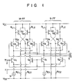
- Fig. 1 shows a conventional frequency divider employing an emitter-coupled logic (to be referred to as ECL hereinafter) type flip-flop circuit (to be referred to as an FF circuit hereinafter).
- ECL emitter-coupled logic
- the ECL FF circuit is constituted by master and slave FF circuits.
- the master FF circuit comprises transistors Q l to Q 8 , resistors R EI , R E2 , R L1 , and R L2 , clock input terminal 12, constant power source 3, and frequency dividing output terminals 1 and 2.
- the slave FF circuit has the same arrangement as the master FF circuit.
- the conventional ECL FF circuit has the following problems. More specifically, in this frequency divider, stray capacitances (not shown) are respectively present between transistors Q 3 and Q 4 , between transistors Q 5 and Q 6 , between the node of the collectors of transistors Q 3 and Q 4 and a ground potential, and between the node of the collectors of transistors Q 5 and Q 6 and the ground potential. Due to the stray capacitances, the transistors cannot satisfactorily effect their operation characteristics (mainly, cut-off frequency fT). Therefore, the maximum frequency characteristics of the transistors are impaired. For this reason, the response property of the frequency divider with respect to a high-frequency clock input, i.e., the follow-up property, is degraded.
- cut-off frequency fT can be improved by improving the manufacturing process.
- the frequency divider itself must also be improved.
- a frequency divider of the present invention comprises a first differential transistor-pair circuit which consists of a pair of emitter-coupled bipolar transistors and performs an inverting switching operation in response to an inverted clock input; a second differential transistor-pair circuit which consists of a pair of bipolar transistors whose emitters are connected to the collector of one transistor provided in the first differential transistor-pair circuit, is switched between enabled and disabled states in response to the differential switching operation of the first differential transistor-pair circuit, and reads data from a data input terminal; a third differential transistor-pair circuit which consists of a pair of bipolar transistors whose emitters are connected to the collector of the other transistor provided in the first differential transistor-pair circuit, and is switched between enabled and disabled states in a complementary manner with the second differential transistor-pair circuit in response to the differential switching operation of the first differential transistor-pair circuit; a data holding transistor circuit which consists of a pair of bipolar transistors whose emitters are cross-coupled to the bases of the transistors provided in the third
- the first differential transistor-pair circuit performs the differential switching operation in response to the inverted clock input so as to enable the second differential transistor-pair circuit and to disable the third differential transistor-pair circuit.
- data input to the second differential transistor-pair circuit is read.
- the second differential transistor-pair circuit When the inverted clock input is inverted, the second differential transistor-pair circuit is disabled, and the third differential transistor-pair circuit is enabled. In this state, the data read by the third differential transistor-pair circuit and the data holding transistor circuit is held. As a result, a data output from the third differential transistor-pair circuit is frequency-divided.
- the frequency divider of the present invention a stray capacitance is inevitably present between a ground potential and the node of the collectors of the bipolar transistors constituting the second and third differential transistor-pair circuits. Therefore, in the frequency divider of the present invention, the first and second peaking circuits are caused to generate an inductive impedance in a predetermined high-frequency range, thereby eliminating the adverse influence of the stray capacitance present on the collector side of the transistors of the differential transistor-pair circuits.
- cut-off frequency fT of bipolar transistors used in the frequency divider can be increased.
- the maximum operation frequency of the transistors can be increased up to a high-frequency range.
- the frequency divider of the present invention can perform a frequency-dividing operation with good response and follow-up properties with respect to a high-frequency input.
- circuit arrangement itself is improved without improving the manufacturing process in order to improve the maximum operation frequency characteristics of the frequency divider.
- NPN bipolar transistors (to be referred to simply as transistors hereinafter) Q 1 , Q 2 , Q 3 , Q 4 , Q 5 , and Q 6 respectively constitute differential transistor-pair circuits.
- the bases of transistors Q 1 and Q 2 are connected to inverted clock T input terminal 2 and clock T input terminal 1.
- the emitters of transistors Q 1 and Q 2 are connected to a V EE power source terminal (normally a ground terminal) at the low potential side through constant current source 3.
- the emitters of transistors Q 3 and Q 5 are connected to the collector of transistor Q 1 .
- the base of transistor Q 3 is connected to inverted data D input terminal 7.
- the base of transistor Q 5 is connected to data input D terminal 6.
- the emitters of transistors Q 4 and Q 6 are connected to the collector of transistor Q 2 .
- the bases of transistors Q 4 and Q 6 are connected to inverted data Q output terminal 9 and data output Q terminal 8, respectively, and are also connected to the V EE power source terminal through resistors R E1 and R E2 , respectively.
- the collectors of transistors Q 3 and Q 4 are connected to each other, and form collector common node Nl.
- the collectors of transistors Q 5 and Q 6 are connected, forming collector common node N2.
- the base of transistor Q 7 is connected to collector common node N1, and the emitter of transistor Q 7 is connected to the base of transistor Q 6 .
- the base of transistor Q 8 is connected to collector common node N2, and the emitter of transistor Q 8 is connected to the base of transistor Q 4 .
- the collectors of transistors Q 7 and Q 8 are connected to power source terminal V CC at the high potential.
- Peaking circuit 10 is connected to power source terminal V CC , and also to collector common node Nl by load resistor R L1 .
- Peaking circuit 11 is coupled to power source terminal V CC , and also to collector common node N2 by load resistor R L2 .
- collector load resistor R C1 for transistor Qg, the collector and emitter of transistor Qg are series- connected between power source terminal V CC and load resistor R L1 .
- the base of transistor Q 9 is connected to power source terminal V CC by base current limiting resistor R Bl .
- peaking circuit 11 comprises transistor Q 10 , collector load resistor Rc 2 , and base current-limiting resistor R B2 , The connection between this and other circuit components is the same as that of peaking circuit 10, and a description thereof is omitted.
- transistor Q 1 When transistor Q 1 is turned on, transistors Q 3 and Q 5 are enabled. Meanwhile, when transistor Q 2 is turned off, transistors Q 4 and Q 6 are disabled.
- inverted data input D is at "0" level and data input D is at "1" level, as described above, transistor Q 3 , is turned off, and transistor Q 5 is turned on.
- transistors Q 3 and Q 5 are disabled, and transistors Q 4 and Q 5 are enabled.
- Data read at collector common nodes Nl and N2 are held by transistors Q 7 , Q 8 , Q 4 , and Q 6 , respectively.
- Transistor Q 7 is turned on and transistor Q 8 is turned off in accordance with read data "1" and "0" read at collector common nodes N1 and N2.
- peaking circuit 10 consisting of load transistor Qg, collector load resistor R C1 , and base current-limiting resistor R B1 has an impedance representing an inductive property in the emitter direction of transistor Qg in a predetermined high-frequency range. More specifically, peaking circuit 10 has peaking characteristics.
- peaking circuits 10 and 11 have the peaking characteristics, the adverse influence of stray capacitances present between collector common nodes Nl and N2, on the one hand, and the ground terminal, on the other, is eliminated.
- the frequency characteristics of bipolar transistors used in the FF circuit in particular, cut-off frequency fT, is improved, and a free-running oscillation frequency as a maximum operation frequency, can be greatly improved.
- collector load resistors R C1 and R C2 can be omitted from peaking circuits 10 and 11.
- npn transistors used in the FF circuit can be replaced with pnp transistors, and the relationship between power source potentials can be inverted.
- Fig. 4 is a circuit diagram showing an ECL type frequency divider using the FF circuit shown in Fig. 2.
- Master FF circuit M-FF and slave FF circuit S-FF have the same configuration as that of the FF circuit shown in Fig. 2.
- data output terminals 8 and 9 of master FF circuit M-FF are respectively connected in correspondence with data input terminals 7 and 6 of slave FF circuit S-FF.
- Clock inputs T and R are input in correspondence with the bases of transistors Q 1 and Q2 constituting the differential transistor pair circuit of slave FF circuit S-FF.
- Data output terminals of slave FF circuit S-FF are feedback-connected in correspondence with data input terminals 6 and 7 of master FF circuit M-FF, so as to serve as frequency-dividing output terminals 4 and 5.
- the frequency-dividing operation of the frequency divider shown in Fig. 4 is known to those skilled in the art, and is performed as shown in the timing chart shown in Fig. 5, so that clock inputs T and T are frequency divided to obtain frequency-divided outputs Q and 5. Since the frequency divider shown in F ig. 4 also has peaking circuits 10 and 11, the maximum operation-frequencies of master FF circuit M-FF and slave FF circuit S-FF are high, and the maximum operation-frequency of the frequency divider is also high. Thus, a stable frequency-dividing operation can be performed with respect to a clock input at 1 GHz or higher.
Landscapes
- Engineering & Computer Science (AREA)
- Power Engineering (AREA)
- Manipulation Of Pulses (AREA)
Applications Claiming Priority (2)
| Application Number | Priority Date | Filing Date | Title |
|---|---|---|---|
| JP66268/86 | 1986-03-25 | ||
| JP61066268A JPS62222712A (ja) | 1986-03-25 | 1986-03-25 | フリツプフロツプ回路 |
Publications (2)
| Publication Number | Publication Date |
|---|---|
| EP0239073A2 true EP0239073A2 (de) | 1987-09-30 |
| EP0239073A3 EP0239073A3 (en) | 1988-07-27 |
Family
ID=13310925
Family Applications (1)
| Application Number | Title | Priority Date | Filing Date |
|---|---|---|---|
| EP87104315A Withdrawn EP0239073A3 (en) | 1986-03-25 | 1987-03-24 | Frequency divider |
Country Status (2)
| Country | Link |
|---|---|
| EP (1) | EP0239073A3 (de) |
| JP (1) | JPS62222712A (de) |
Cited By (2)
| Publication number | Priority date | Publication date | Assignee | Title |
|---|---|---|---|---|
| EP0403215A3 (de) * | 1989-06-12 | 1993-07-21 | Nec Corporation | Flip-flop-Schaltkreis |
| CN104734671A (zh) * | 2014-10-10 | 2015-06-24 | 中国电子科技集团公司第二十四研究所 | 基于SiGe BiCMOS工艺的ECL触发器 |
Families Citing this family (1)
| Publication number | Priority date | Publication date | Assignee | Title |
|---|---|---|---|---|
| DE10038905C2 (de) | 2000-08-09 | 2003-04-17 | Atmel Germany Gmbh | Verfahren zur Erhöhung der Grenzfrequenz bei Flip-Flops |
Family Cites Families (2)
| Publication number | Priority date | Publication date | Assignee | Title |
|---|---|---|---|---|
| US4100055A (en) * | 1977-06-10 | 1978-07-11 | Varian Associates, Inc. | Target profile for sputtering apparatus |
| PT74627B (en) * | 1981-04-01 | 1983-08-22 | Rca Corp | Flip-flop circuit |
-
1986
- 1986-03-25 JP JP61066268A patent/JPS62222712A/ja active Pending
-
1987
- 1987-03-24 EP EP87104315A patent/EP0239073A3/en not_active Withdrawn
Cited By (3)
| Publication number | Priority date | Publication date | Assignee | Title |
|---|---|---|---|---|
| EP0403215A3 (de) * | 1989-06-12 | 1993-07-21 | Nec Corporation | Flip-flop-Schaltkreis |
| CN104734671A (zh) * | 2014-10-10 | 2015-06-24 | 中国电子科技集团公司第二十四研究所 | 基于SiGe BiCMOS工艺的ECL触发器 |
| CN104734671B (zh) * | 2014-10-10 | 2017-06-16 | 中国电子科技集团公司第二十四研究所 | 基于SiGe BiCMOS工艺的ECL触发器 |
Also Published As
| Publication number | Publication date |
|---|---|
| EP0239073A3 (en) | 1988-07-27 |
| JPS62222712A (ja) | 1987-09-30 |
Similar Documents
| Publication | Publication Date | Title |
|---|---|---|
| US4560888A (en) | High-speed ECL synchronous logic circuit with an input logic circuit | |
| US5001361A (en) | Master-slave flip-flop circuit | |
| KR910009086B1 (ko) | 출력회로 | |
| US4607177A (en) | Circuit arrangement for conversion TTL logic signals to ECL logic signals | |
| US4622475A (en) | Data storage element having input and output ports isolated from regenerative circuit | |
| US6268752B1 (en) | Master-slave flip-flop circuit | |
| US5900760A (en) | Low voltage ECL latch and flip-flop | |
| US4309625A (en) | Flip-flop circuit | |
| JPH09238054A (ja) | タイマー回路 | |
| JP2546004B2 (ja) | レベル変換回路 | |
| JP2747467B2 (ja) | スタティック型フリップフロップ回路 | |
| JPH0738580B2 (ja) | エミッタ結合論理回路 | |
| JPS6316047B2 (de) | ||
| WO2004004122A1 (ja) | スタティック型フリップフロップ回路 | |
| JPH08195651A (ja) | 差動型rsラッチ回路 | |
| JPH0666654B2 (ja) | フリツプフロツプ | |
| JP3340142B2 (ja) | ダイナミック型分周器 | |
| JP2933022B2 (ja) | フリップフロップ回路 | |
| US3300654A (en) | Schmitt trigger with active collector to base coupling | |
| JPS63240117A (ja) | 半導体集積回路装置 | |
| JPH10135792A (ja) | フリップフロップ回路 | |
| US5541545A (en) | High speed bipolar D latch circuit with reduced latch clocking output corruption | |
| JPH06209237A (ja) | 記憶セル | |
| JP2953859B2 (ja) | リセット付ディレイフリップフロップ回路 | |
| JP2776201B2 (ja) | フリップフロップ回路 |
Legal Events
| Date | Code | Title | Description |
|---|---|---|---|
| PUAI | Public reference made under article 153(3) epc to a published international application that has entered the european phase |
Free format text: ORIGINAL CODE: 0009012 |
|
| 17P | Request for examination filed |
Effective date: 19870421 |
|
| AK | Designated contracting states |
Kind code of ref document: A2 Designated state(s): DE FR GB |
|
| PUAL | Search report despatched |
Free format text: ORIGINAL CODE: 0009013 |
|
| AK | Designated contracting states |
Kind code of ref document: A3 Designated state(s): DE FR GB |
|
| 17Q | First examination report despatched |
Effective date: 19891011 |
|
| STAA | Information on the status of an ep patent application or granted ep patent |
Free format text: STATUS: THE APPLICATION IS DEEMED TO BE WITHDRAWN |
|
| 18D | Application deemed to be withdrawn |
Effective date: 19900422 |
|
| RIN1 | Information on inventor provided before grant (corrected) |
Inventor name: OIDA, YOSHIOC/O PATENT DIVISION |