EP0239078A2 - System zur Registersicherstellung/-umspeicherung - Google Patents
System zur Registersicherstellung/-umspeicherung Download PDFInfo
- Publication number
- EP0239078A2 EP0239078A2 EP87104338A EP87104338A EP0239078A2 EP 0239078 A2 EP0239078 A2 EP 0239078A2 EP 87104338 A EP87104338 A EP 87104338A EP 87104338 A EP87104338 A EP 87104338A EP 0239078 A2 EP0239078 A2 EP 0239078A2
- Authority
- EP
- European Patent Office
- Prior art keywords
- register
- processing unit
- task
- command
- additional processing
- Prior art date
- Legal status (The legal status is an assumption and is not a legal conclusion. Google has not performed a legal analysis and makes no representation as to the accuracy of the status listed.)
- Granted
Links
Images


Classifications
-
- G—PHYSICS
- G06—COMPUTING OR CALCULATING; COUNTING
- G06F—ELECTRIC DIGITAL DATA PROCESSING
- G06F9/00—Arrangements for program control, e.g. control units
- G06F9/06—Arrangements for program control, e.g. control units using stored programs, i.e. using an internal store of processing equipment to receive or retain programs
- G06F9/30—Arrangements for executing machine instructions, e.g. instruction decode
- G06F9/38—Concurrent instruction execution, e.g. pipeline or look ahead
- G06F9/3877—Concurrent instruction execution, e.g. pipeline or look ahead using a secondary processor, e.g. coprocessor
-
- G—PHYSICS
- G06—COMPUTING OR CALCULATING; COUNTING
- G06F—ELECTRIC DIGITAL DATA PROCESSING
- G06F9/00—Arrangements for program control, e.g. control units
- G06F9/06—Arrangements for program control, e.g. control units using stored programs, i.e. using an internal store of processing equipment to receive or retain programs
- G06F9/46—Multiprogramming arrangements
- G06F9/461—Saving or restoring of program or task context
Definitions
- the present invention relates to an additional processing unit (which will be called a "slave processor” hereinafter) coupled to a microprocessor and, more particularly, to a register saving/restoring system for saving and restoring data in a register provided in the slave processor into and out of a main memory unit when tasks are switched.
- a slave processor which will be called a "slave processor” hereinafter
- a register saving/restoring system for saving and restoring data in a register provided in the slave processor into and out of a main memory unit when tasks are switched.
- the microprocessor is frequently composed of a plurality of chips when attempts are made to extend its function, because all the functions cannot be integrated into a single chip.
- a microprocessor system is currently constructed by coupling a chip for a central processing system (which will be abbreviated into "CPU") and one or more chips for slave processor through a local bus.
- CPU central processing system
- the CPU itself has a function of the microprocessor. But, the function can be easily extended and the operation can be executed at a high speed by coupling the CPU with one or more slave processors and causing these processors to execute the extended commands of the CPU.
- FIG. 1 A CPU 109, eight slave processors 101 to 108 and a main memory unit 140 are coupled through a local bus 130 to construct altogether a microprocessor 100.
- the CPU 109 contains at least one register 119, and each of the slave processors 101 to 108 contains at least one register 111 to 118.
- Commands for the microprocessor 100 are classified into nine sets: one set to be executed by the CPU 109 and eight sets to be executed by the slave processors 101 to 108.
- the set of commands to be executed by the CPU 109 uses the register 119 in the CUP 109 but not the registers 111 to 118 in the slave processors 101 to 108.
- the set of commands to be executed by the slave processor 101 uses both the register 111 in the slave processor 101 and the register 119 in the CPU 109 but not the registers 112 to 118 in the remaining slave processors 102 to 108. This usage also applies to the slave processors 102 to 108.
- the major task environments are registers belonging to a microprocessor.
- the registers 119 and 111 to 118 can create the task environments.
- the switching of these task environments is conducted by saving the content of a register or the environment of a previous task in a register save area which is prepared for each task on the main memory unit 140 and by restoring the once saved register content into the registers 119 and 111 to 118 out of the register save area of the next task to be switched.
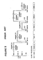
- FIG. 2 shows the case in which tasks A, B and C are to be asynchronously switched. All the programs of the tasks A, B and C contain the commands to the CPU 109 and the slave processors 111 to 118. At the instants of task switchings 201, 202 and 203, therefore, the register saving/restoring processes are conducted for the registers 111 to 118.
- the microprocessor of the prior art described above and constructed of the CPU and one or more slave processors is accompanied by the following defect: Although the programs of individual tasks contain commands to the slave processors, even the registers of the slave processors unused in the task switching are subjected to the saving/restoring processes, too, in case the slave processors are not used in a segment continuing from a current task switching to a subsequent task switching. This defect becomes more serious from a greater number of slave processors coupled to the CPU and each containing a register therein, so that the time period needed for the task switching becomes the longer.
- register saving/restoring processings thus conducted unnecessarily are caused by the fact that they are conducted at any task switching for all the slave processors that may possibly be used for a subsequent task.
- a slave processor register saving/restoring system for a processor system having a CPU and one or more slave processors, comprising: first means for storing the descriptor of the last task having been executed in each of the slave processors; second means for comparing the content of the descriptor of a current task being executed by a CPU with the content of the first means; and third means for switching, if the comparison results in inconsistency, the task environment of a target one of the slave processors immediately before the target slave processor is used.
- a register saving/restoring system comprising: first means for storing the descriptor of a task being executed by the central processing unit; second means for storing the descriptor of a task to be executed by one of the additional processing units; and third means for judging whether or not the contents of the first means and the second means are consistent, wherein the central processing unit defers the execution of a command to each of the additional processing units by causing the third means to conduct the judgement such that, if the judgement reveals an inconsistency, it saves the content of the register resource of the additional processing unit into the register save area of the main memory unit and restores the environment of a task indicated by the first means out of the register save area of the main memory unit into the register resource of a corresponding one of the additional
- a register saving/restoring process comprising the steps of: storing the descriptor of a task being executed by the central processing unit; storing the descriptor of a task to be executed by one of the additional processing units; judging whether or not the contents of the executed task and the task to be executed are consistent; if the judgement reveals an inconsistency, saving the content of the register resource of each of the additional processing units into the register save area of the main memory unit, restoring the environment of the task to be executed out of the register save area of the main memory unit into the register resource of a corresponding one of the additional processing units, and executing a command to the corresponding additional processing unit; and if the judgement reveals a consistency, executing the command immediately without saving the register resources of the additional processing units.
- the registers of the slave processors are neither saved nor restored when the CPU switches tasks, but the descriptor of the task having used one slave processor the most recently and the descriptor of a task being executed by the CPU are compared so that the slave processor registers are saved and restored, only if the descriptors are different, to avoid the waste register saving/restoring processing.
- the data processing system incorporating the register saving/restoring system of the present invention can operate at a high speed.
- Figure 3 shows a data processing system having a register saving/restoring (storing/loading) system according to one embodiment of the present invention.
- the microprocessor shown in Figure 3 is constructed by coupling a CPU 109, a main memory unit 140 and a plurality of, for example, eight slave processors (but only one slave processor 101 is shown and the remaining slave processors are not shown) through a local bus 130.
- the CPU 109 is composed of an operation unit 129 which includes at least one register 119
- the slave processor 101 is composed of an operation unit 121 which includes at least one register 111.
- a task register 139 built in the CPU 109 is used to store the descriptor of a task being executed by the CPU 109
- an owner register 151 built in the slave processor 101 is used to store the descriptor of a task having lastly used the slave processor 101.
- a check port 161 for copying the content of the task register 139
- a comparator 171 for detecting the coincidence between the contents of the owner register 151 and the check port 161
- a command port 131 for receiving a command to be executed by the slave processor 101 from the local bus 130 and addressing it
- a trigger port 141 for beginning the execution of a command addressed by the command port 131.
- each of the remaining seven slave processors is also composed of an operation unit having an internal register, a command port, a trigger port, an owner register, a check port, and a comparator, respectively, similarly to the slave processor 101.
- the remaining seven slave processors are indicated by Reference Numerals 102 to 108, and their associated command ports, trigger ports, the owner registers and the check ports and the comparators are designated by Reference Numerals 132-138, 142-148, 152-158, 162-168 and 172-178, respectively.
- register saving/restoring (storing/loading) system of the present invention will be described in the following with reference to Figures 4A, 4B and 4C.
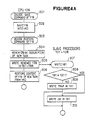
- FIG 4A shows the operations of the CPU 109 and the slave processors 101 to 108 when the CPU 109 switches tasks.
- the CPU 109 decodes (at a step 301) its register save command, it saves (or stores) (at a step 302) the content of its register 119 in a register save area of the main memory unit 140 through the local bus 130.
- the CPU 109 decodes (at a step 303) its register restore command, it renews (at a step 304) its task register 139 by the descriptor of a new task designated by the command 303. Then, the CPU 109 writes (at a step 305) the renewed content of the task register 139 simultaneously in the check ports 161 to 168 of all the slave processors 101 to 108 through the local bus 130, and (at a step 306) restores (or loads) the register content out of the register save area of the main memory unit 140 for a new task into the register 119 through the local bus 130.
- the slave processor 101 uses its comparator 171 to compare (at a step 308) the contents of the check port 161 and the owner register 151. If NO (that is, if the contents are different), the slave processor 101 writes (at a step 309) "TRAP" (i.e., the content indicating that the current task being executed by the CPU 109 and the last task having lastly used the slave processor 109 are different) in the trigger port 141. If YES, the slave processor 101 writes (at a step 310) "OK" in the trigger port 141.
- the aforementioned processings on the slave processor 101 are simultaneously executed on the remaining slave processors 102 to 108. By the processings described above, the task environment of the CPU 109 has been switched to a new task, but the task environments of the slave processors 101 to 108 have not been switched yet.
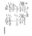
- FIG 4B shows how a command to the slave processor 101 is executed by the CPU 109 and the slave processor 101.
- the CPU 109 decodes (at a step 320) the command to the slave processor 101, it writes (at a step 321) the command code in its command port 131 through the local bus 130.
- the slave processor 101 writes (at a step 322) the command in the command port 131 and decodes (at a step 323) the written command but does not execute it.
- the CPU 109 reads (at a step 324) the content of the trigger port 141. If the content is "OK” the CPU continue (at a step 325) the support of the slave processor 101. If the content is "TRAP", on the contrary, the CPU 109 interrupts the command to the slave processor 101 to shift (at a step 326) the control to a trap handler.
- the slave processor 101 reads (at a step 327) the content of the trigger port 141. If this content is "OK”, the slave processor 101 executes (at a step 328) the decoded command. If the content is "TRAP”, on the contrary, the slave processor 101 interrupts (at a step 329) the execution of the command while setting the content of the trigger port 141 at "OK".
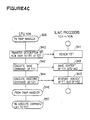
- FIG. 4C shows the task environment switching operations of the slave processor 101.
- the CPU 109 having its control shifted (at the step 326) to the trap handler, transfers (at a step 340) the content of the task register 139, i.e., the descriptor of the current task (i.e., a CPU task renewed (at a step 341) by the slave processor 101) being executed by the CPU 109 to the owner register 151 of the slave processor 101 through the local bus 130.
- the CPU 109 causes the slave processor 101 to execute (at a step 342) the register save command and transfers (at a step 343) the content of the register 111 to the register save area of the main memory unit 140. Then, the CPU 109 causes the slave processor 101 to execute (at a step 344) the register restore command and restores (at a step 345) the content of the register 111 out of the register save area for the new task. After this execution, the CPU 109 returns (at a step 346) its control from the trap handler.
- Both the CPU 109 thus having ended the saving/restoring processing of the register 111 of the slave processor 101 and this slave processor 101 re-execute (at a step 350) the command (of the step 320) to the slave processor 101 in which TRAP has occurred in its trigger port 141.
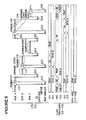
- FIG 5 shows the operations of the CPU 109 and the slave processors 101 to 108 in the same task switchings as those of Figure 2.
- the slave processors 101 to 108 are initially set in the environment of a task D whereas the CPU is initially set in the environment of a task A so that the individual trigger ports 141 to 148 are at the "TRAP" content.
- the CPU 109 executes a command 231 to the slave processor 102, its control is shifted (at a step 221) to te trap handler because the trigger port 142 has the "TRAP" content.
- the task environment of the slave processor 102 is switched to the same task A as that of the CPU 109 so that the content of the owner register 152 becomes the descriptor of the task A whereas the trigger portion 142 takes the content "OK". After this, the interrupted command 231 to the slave processor 102 is re-executed.
- the task environments of the slave processor 102 before and after the switching remain in the task A whereas the task environment of the CPU 109 immediately after the switching is switched to a task B so that the trigger port 142 takes the content "TRAP".
- the trigger port 142 takes the content "OK" so that the command 234 is executed without any TRAP (i.e., without any interchange of the task environments).
- the embodiment thus far described realizes the most proper register saving/restoring processing at a unit of each slave processor.
- the register of each slave processor may be divided into plural blocks so that the register saving/restoring processing may be controlled at a unit of each block.
- the register saving/restoring system has means for comparing the descriptor of the last task having used one slave processor most recently and the descriptor of a current task being executed by the CPU so that the register saving/restoring processing of the slave processor is not conducted when the CPU switches the task but if the tasks of the CPU and the slave processor are different while the slave processor is being used, thus bringing about an effect that the waste register saving/restoring processing of the slave processor need not be conducted.
- the microprocessor includes the eight slave processors, but the present invention is not limited to the eight slave processors.
- the microprocessor can comprises a plurality of slave processors of the number other than eight.
Landscapes
- Engineering & Computer Science (AREA)
- Software Systems (AREA)
- Theoretical Computer Science (AREA)
- Physics & Mathematics (AREA)
- General Engineering & Computer Science (AREA)
- General Physics & Mathematics (AREA)
- Multi Processors (AREA)
Applications Claiming Priority (2)
| Application Number | Priority Date | Filing Date | Title |
|---|---|---|---|
| JP61066508A JPS62221732A (ja) | 1986-03-24 | 1986-03-24 | 情報処理装置 |
| JP66508/86 | 1986-03-24 |
Publications (3)
| Publication Number | Publication Date |
|---|---|
| EP0239078A2 true EP0239078A2 (de) | 1987-09-30 |
| EP0239078A3 EP0239078A3 (en) | 1988-01-27 |
| EP0239078B1 EP0239078B1 (de) | 1991-10-16 |
Family
ID=13317845
Family Applications (1)
| Application Number | Title | Priority Date | Filing Date |
|---|---|---|---|
| EP87104338A Expired EP0239078B1 (de) | 1986-03-24 | 1987-03-24 | System zur Registersicherstellung/-umspeicherung |
Country Status (4)
| Country | Link |
|---|---|
| US (1) | US4851992A (de) |
| EP (1) | EP0239078B1 (de) |
| JP (1) | JPS62221732A (de) |
| DE (1) | DE3773717D1 (de) |
Cited By (3)
| Publication number | Priority date | Publication date | Assignee | Title |
|---|---|---|---|---|
| EP0333366A3 (de) * | 1988-03-18 | 1991-05-02 | Digital Equipment Corporation | Kontextumschaltungsverfahren und -anordnung zur Verwendung in einem Vektorverarbeitungssystem |
| EP0333365A3 (de) * | 1988-03-18 | 1991-05-08 | Digital Equipment Corporation | Verfahren und Anordnung zur Verarbeitung von asynchronen Speicherverwaltungsausnahmen durch einen Vektorprozessor |
| US9043806B2 (en) | 2010-04-30 | 2015-05-26 | Nec Corporation | Information processing device and task switching method |
Families Citing this family (13)
| Publication number | Priority date | Publication date | Assignee | Title |
|---|---|---|---|---|
| US5210874A (en) * | 1988-03-22 | 1993-05-11 | Digital Equipment Corporation | Cross-domain call system in a capability based digital data processing system |
| GB2254714B (en) * | 1988-03-22 | 1992-12-23 | Digital Equipment Corp | Cross-domain call system in a capability based digital data processing system |
| JPH0277870A (ja) * | 1988-06-30 | 1990-03-16 | Mitsubishi Electric Corp | 並列計算機システム |
| JPH03154105A (ja) * | 1989-11-10 | 1991-07-02 | Toshiba Mach Co Ltd | Ncプログラム作成装置 |
| JPH0495137A (ja) * | 1990-08-07 | 1992-03-27 | Nec Corp | オペレーティングシステムのコンテキスト切替方式 |
| US5455935A (en) * | 1991-05-31 | 1995-10-03 | Tandem Computers Incorporated | Clock synchronization system |
| IL124594A0 (en) * | 1998-05-21 | 1998-12-06 | Nds Ltd | Context saving system |
| US7093260B1 (en) * | 2000-05-04 | 2006-08-15 | International Business Machines Corporation | Method, system, and program for saving a state of a task and executing the task by a processor in a multiprocessor system |
| US7191313B2 (en) * | 2001-08-28 | 2007-03-13 | Sony Corporation | Microprocessor |
| US7434222B2 (en) * | 2001-12-20 | 2008-10-07 | Infineon Technologies Ag | Task context switching RTOS |
| EP1622009A1 (de) * | 2004-07-27 | 2006-02-01 | Texas Instruments Incorporated | JSM-Architektur und Systeme |
| US7739435B2 (en) * | 2006-12-29 | 2010-06-15 | Texas Instruments Incorporated | System and method for enhancing I2C bus data rate |
| CN113254070B (zh) * | 2020-02-07 | 2024-01-02 | 阿里巴巴集团控股有限公司 | 加速单元、片上系统、服务器、数据中心和相关方法 |
Family Cites Families (11)
| Publication number | Priority date | Publication date | Assignee | Title |
|---|---|---|---|---|
| US3643227A (en) * | 1969-09-15 | 1972-02-15 | Fairchild Camera Instr Co | Job flow and multiprocessor operation control system |
| DE2214240C2 (de) * | 1972-03-23 | 1974-03-28 | Siemens Ag, 1000 Berlin U. 8000 Muenchen | Verfahren zur Abspeicherung von Steuerdaten bei Programmunterbrechung in einem Verarbeitungssystem |
| JPS4995548A (de) * | 1973-01-12 | 1974-09-10 | ||
| JPS5841538B2 (ja) * | 1975-12-04 | 1983-09-13 | 株式会社東芝 | マルチプロセツサシステム ノ ユウセンセイギヨホウシキ |
| US4333144A (en) * | 1980-02-05 | 1982-06-01 | The Bendix Corporation | Task communicator for multiple computer system |
| US4414624A (en) * | 1980-11-19 | 1983-11-08 | The United States Of America As Represented By The Secretary Of The Navy | Multiple-microcomputer processing |
| US4430707A (en) * | 1981-03-05 | 1984-02-07 | Burroughs Corporation | Microprogrammed digital data processing system employing multi-phase subroutine control for concurrently executing tasks |
| US4685125A (en) * | 1982-06-28 | 1987-08-04 | American Telephone And Telegraph Company | Computer system with tasking |
| JPS60195646A (ja) * | 1984-03-16 | 1985-10-04 | Hitachi Ltd | デ−タ処理装置 |
| JPS6159539A (ja) * | 1984-08-30 | 1986-03-27 | Nec Corp | サブプロセツサのレジスタ退避/復帰方式 |
| US4736318A (en) * | 1985-03-01 | 1988-04-05 | Wang Laboratories, Inc. | Data processing system having tunable operating system means |
-
1986
- 1986-03-24 JP JP61066508A patent/JPS62221732A/ja active Granted
-
1987
- 1987-03-24 EP EP87104338A patent/EP0239078B1/de not_active Expired
- 1987-03-24 US US07/029,569 patent/US4851992A/en not_active Expired - Fee Related
- 1987-03-24 DE DE8787104338T patent/DE3773717D1/de not_active Expired - Lifetime
Cited By (3)
| Publication number | Priority date | Publication date | Assignee | Title |
|---|---|---|---|---|
| EP0333366A3 (de) * | 1988-03-18 | 1991-05-02 | Digital Equipment Corporation | Kontextumschaltungsverfahren und -anordnung zur Verwendung in einem Vektorverarbeitungssystem |
| EP0333365A3 (de) * | 1988-03-18 | 1991-05-08 | Digital Equipment Corporation | Verfahren und Anordnung zur Verarbeitung von asynchronen Speicherverwaltungsausnahmen durch einen Vektorprozessor |
| US9043806B2 (en) | 2010-04-30 | 2015-05-26 | Nec Corporation | Information processing device and task switching method |
Also Published As
| Publication number | Publication date |
|---|---|
| US4851992A (en) | 1989-07-25 |
| EP0239078A3 (en) | 1988-01-27 |
| JPS62221732A (ja) | 1987-09-29 |
| JPH0521251B2 (de) | 1993-03-23 |
| EP0239078B1 (de) | 1991-10-16 |
| DE3773717D1 (de) | 1991-11-21 |
Similar Documents
| Publication | Publication Date | Title |
|---|---|---|
| US4851992A (en) | Register/saving/restoring system for saving and restoring data in a register of a slave processor | |
| US5386563A (en) | Register substitution during exception processing | |
| US5613114A (en) | System and method for custom context switching | |
| US6209085B1 (en) | Method and apparatus for performing process switching in multiprocessor computer systems | |
| US5161226A (en) | Microprocessor inverse processor state usage | |
| FI78993B (fi) | Oevervakare av driftsystem. | |
| US5428779A (en) | System and method for supporting context switching within a multiprocessor system having functional blocks that generate state programs with coded register load instructions | |
| US3984820A (en) | Apparatus for changing the interrupt level of a process executing in a data processing system | |
| US4020471A (en) | Interrupt scan and processing system for a data processing system | |
| US5148544A (en) | Apparatus and method for control of asynchronous program interrupt events in a data processing system | |
| EP0285310A2 (de) | Vorrichtung zur Sicherung und Rückspeicherung einer Registerinformation | |
| US4949241A (en) | Microcomputer system including a master processor and a slave processor synchronized by three control lines | |
| GB2348306A (en) | Batch processing of tasks in data processing systems | |
| JPH0544054B2 (de) | ||
| EP0290942B1 (de) | Gastmaschinenablaufsteuerungssystem für virtuelles Maschinensystem | |
| JP2007500394A (ja) | 優先レベル毎に異なるレジスタセットが関連付けられたプログラマブル優先レベルを有する割り込み構造を備えたマイクロコントローラ | |
| US5491826A (en) | Microprocessor having register bank and using a general purpose register as a stack pointer | |
| JPH02242434A (ja) | タスクのスケジューリング方法 | |
| JPS6393055A (ja) | 実時間型ガ−ベジコレクシヨン支援装置 | |
| AU626067B2 (en) | Apparatus and method for control of asynchronous program interrupt events in a data processing system | |
| US6708259B1 (en) | Programmable wake up of memory transfer controllers in a memory transfer engine | |
| US20030126520A1 (en) | System and method for separating exception vectors in a multiprocessor data processing system | |
| US20060193260A1 (en) | Preemptive packet flow controller | |
| US20030014474A1 (en) | Alternate zero overhead task change circuit | |
| JPS6097440A (ja) | 仮想多重プロセツサ装置 |
Legal Events
| Date | Code | Title | Description |
|---|---|---|---|
| PUAI | Public reference made under article 153(3) epc to a published international application that has entered the european phase |
Free format text: ORIGINAL CODE: 0009012 |
|
| 17P | Request for examination filed |
Effective date: 19870324 |
|
| AK | Designated contracting states |
Kind code of ref document: A2 Designated state(s): DE FR GB |
|
| PUAL | Search report despatched |
Free format text: ORIGINAL CODE: 0009013 |
|
| AK | Designated contracting states |
Kind code of ref document: A3 Designated state(s): DE FR GB |
|
| 17Q | First examination report despatched |
Effective date: 19900313 |
|
| GRAA | (expected) grant |
Free format text: ORIGINAL CODE: 0009210 |
|
| AK | Designated contracting states |
Kind code of ref document: B1 Designated state(s): DE FR GB |
|
| REF | Corresponds to: |
Ref document number: 3773717 Country of ref document: DE Date of ref document: 19911121 |
|
| ET | Fr: translation filed | ||
| PLBE | No opposition filed within time limit |
Free format text: ORIGINAL CODE: 0009261 |
|
| STAA | Information on the status of an ep patent application or granted ep patent |
Free format text: STATUS: NO OPPOSITION FILED WITHIN TIME LIMIT |
|
| 26N | No opposition filed | ||
| PGFP | Annual fee paid to national office [announced via postgrant information from national office to epo] |
Ref country code: GB Payment date: 19940318 Year of fee payment: 8 |
|
| PGFP | Annual fee paid to national office [announced via postgrant information from national office to epo] |
Ref country code: FR Payment date: 19940321 Year of fee payment: 8 |
|
| PGFP | Annual fee paid to national office [announced via postgrant information from national office to epo] |
Ref country code: DE Payment date: 19940524 Year of fee payment: 8 |
|
| PG25 | Lapsed in a contracting state [announced via postgrant information from national office to epo] |
Ref country code: GB Effective date: 19950324 |
|
| GBPC | Gb: european patent ceased through non-payment of renewal fee |
Effective date: 19950324 |
|
| PG25 | Lapsed in a contracting state [announced via postgrant information from national office to epo] |
Ref country code: FR Free format text: LAPSE BECAUSE OF NON-PAYMENT OF DUE FEES Effective date: 19951130 |
|
| PG25 | Lapsed in a contracting state [announced via postgrant information from national office to epo] |
Ref country code: DE Effective date: 19951201 |
|
| REG | Reference to a national code |
Ref country code: FR Ref legal event code: ST |