EP0241669A1 - Procédé de fixage et d'alignement d'une pièce terminale d'une fibre de verre - Google Patents
Procédé de fixage et d'alignement d'une pièce terminale d'une fibre de verre Download PDFInfo
- Publication number
- EP0241669A1 EP0241669A1 EP87102149A EP87102149A EP0241669A1 EP 0241669 A1 EP0241669 A1 EP 0241669A1 EP 87102149 A EP87102149 A EP 87102149A EP 87102149 A EP87102149 A EP 87102149A EP 0241669 A1 EP0241669 A1 EP 0241669A1
- Authority
- EP
- European Patent Office
- Prior art keywords
- base
- end section
- holding body
- deformed
- glass fiber
- Prior art date
- Legal status (The legal status is an assumption and is not a legal conclusion. Google has not performed a legal analysis and makes no representation as to the accuracy of the status listed.)
- Withdrawn
Links
- 238000000034 method Methods 0.000 title claims abstract description 17
- 239000003365 glass fiber Substances 0.000 title claims abstract description 14
- 229910000679 solder Inorganic materials 0.000 claims abstract description 9
- 239000002184 metal Substances 0.000 claims abstract description 7
- 229910052751 metal Inorganic materials 0.000 claims abstract description 7
- 230000001681 protective effect Effects 0.000 claims abstract description 7
- 230000005693 optoelectronics Effects 0.000 claims abstract description 5
- 239000000463 material Substances 0.000 claims abstract description 4
- 229910001218 Gallium arsenide Inorganic materials 0.000 claims abstract description 3
- 239000007787 solid Substances 0.000 claims abstract description 3
- RYGMFSIKBFXOCR-UHFFFAOYSA-N Copper Chemical compound [Cu] RYGMFSIKBFXOCR-UHFFFAOYSA-N 0.000 claims abstract 2
- 238000010276 construction Methods 0.000 claims abstract 2
- 229910052802 copper Inorganic materials 0.000 claims abstract 2
- 239000010949 copper Substances 0.000 claims abstract 2
- 229910052738 indium Inorganic materials 0.000 claims abstract 2
- APFVFJFRJDLVQX-UHFFFAOYSA-N indium atom Chemical compound [In] APFVFJFRJDLVQX-UHFFFAOYSA-N 0.000 claims abstract 2
- 238000004519 manufacturing process Methods 0.000 claims description 5
- 238000004891 communication Methods 0.000 claims description 2
- 239000007788 liquid Substances 0.000 claims description 2
- 239000011241 protective layer Substances 0.000 claims description 2
- 239000013307 optical fiber Substances 0.000 abstract description 2
- 238000006073 displacement reaction Methods 0.000 description 2
- 230000007613 environmental effect Effects 0.000 description 2
- 238000005476 soldering Methods 0.000 description 2
- 239000000853 adhesive Substances 0.000 description 1
- 230000001070 adhesive effect Effects 0.000 description 1
- 239000004161 brilliant blue FCF Substances 0.000 description 1
- 230000007797 corrosion Effects 0.000 description 1
- 238000005260 corrosion Methods 0.000 description 1
- 230000008878 coupling Effects 0.000 description 1
- 238000010168 coupling process Methods 0.000 description 1
- 238000005859 coupling reaction Methods 0.000 description 1
- 238000011161 development Methods 0.000 description 1
- 230000018109 developmental process Effects 0.000 description 1
- 230000007257 malfunction Effects 0.000 description 1
- 230000003287 optical effect Effects 0.000 description 1
- 239000004065 semiconductor Substances 0.000 description 1
- 238000007493 shaping process Methods 0.000 description 1
- 230000006641 stabilisation Effects 0.000 description 1
- 238000011105 stabilization Methods 0.000 description 1
- 239000000126 substance Substances 0.000 description 1
Images
Classifications
-
- G—PHYSICS
- G02—OPTICS
- G02B—OPTICAL ELEMENTS, SYSTEMS OR APPARATUS
- G02B6/00—Light guides; Structural details of arrangements comprising light guides and other optical elements, e.g. couplings
- G02B6/24—Coupling light guides
- G02B6/42—Coupling light guides with opto-electronic elements
- G02B6/4201—Packages, e.g. shape, construction, internal or external details
- G02B6/4202—Packages, e.g. shape, construction, internal or external details for coupling an active element with fibres without intermediate optical elements, e.g. fibres with plane ends, fibres with shaped ends, bundles
-
- G—PHYSICS
- G02—OPTICS
- G02B—OPTICAL ELEMENTS, SYSTEMS OR APPARATUS
- G02B6/00—Light guides; Structural details of arrangements comprising light guides and other optical elements, e.g. couplings
- G02B6/24—Coupling light guides
- G02B6/42—Coupling light guides with opto-electronic elements
- G02B6/4201—Packages, e.g. shape, construction, internal or external details
- G02B6/4219—Mechanical fixtures for holding or positioning the elements relative to each other in the couplings; Alignment methods for the elements, e.g. measuring or observing methods especially used therefor
- G02B6/422—Active alignment, i.e. moving the elements in response to the detected degree of coupling or position of the elements
- G02B6/4226—Positioning means for moving the elements into alignment, e.g. alignment screws, deformation of the mount
-
- G—PHYSICS
- G02—OPTICS
- G02B—OPTICAL ELEMENTS, SYSTEMS OR APPARATUS
- G02B6/00—Light guides; Structural details of arrangements comprising light guides and other optical elements, e.g. couplings
- G02B6/24—Coupling light guides
- G02B6/42—Coupling light guides with opto-electronic elements
- G02B6/4201—Packages, e.g. shape, construction, internal or external details
- G02B6/4219—Mechanical fixtures for holding or positioning the elements relative to each other in the couplings; Alignment methods for the elements, e.g. measuring or observing methods especially used therefor
- G02B6/4236—Fixing or mounting methods of the aligned elements
- G02B6/4238—Soldering
-
- G—PHYSICS
- G02—OPTICS
- G02B—OPTICAL ELEMENTS, SYSTEMS OR APPARATUS
- G02B6/00—Light guides; Structural details of arrangements comprising light guides and other optical elements, e.g. couplings
- G02B6/24—Coupling light guides
- G02B6/42—Coupling light guides with opto-electronic elements
- G02B6/4201—Packages, e.g. shape, construction, internal or external details
- G02B6/4219—Mechanical fixtures for holding or positioning the elements relative to each other in the couplings; Alignment methods for the elements, e.g. measuring or observing methods especially used therefor
- G02B6/4236—Fixing or mounting methods of the aligned elements
- G02B6/4239—Adhesive bonding; Encapsulation with polymer material
Definitions
- the invention is based on the special method defined in the preamble of claim 1, which by itself * DE-A1 34 05 838 is already known.
- a very similar process is already in place * DE-A1 34 31 775 previously known, but not the holding body, but a ductile intermediate part (BS in DE-A1 34 05 838; 9 in DE-A1 34 31 775) is deformed in order to achieve the final precise adjustment.
- the two previously known methods are - in addition to being quite complicatedly designed - fastening arrangements which, after the final adjustment, are still quite sensitive to temperature fluctuations, as a result of which, from time to time, more or less severe misalignments occur which can cause considerable malfunctions.
- the precision of the adjustment of the distance of the tip of the end section (“taper") from the active location of the structure must generally be far less than the precision of the adjustment perpendicular to it , i.e. as the precision of the adjustment perpendicular to the axis direction of the end section.
- the tip of the end section perpendicular to the direction of the axis in a single-mode glass fiber should often be set to an accuracy of ⁇ 0.1 ⁇ m, but the fastening of the end section, for example the soldering or the adhesive, usually warps too much again during curing and thus the adjustment achieved before the fastening hardened is destroyed again.
- the object of the invention * Ensure the adjustment of the tip of the end section perpendicular to the axis direction of the attached glass fiber with high precision, for example largely independent of temperature, and * moreover, this adjustment can be achieved with very little effort is solved by the measures mentioned in claim 1.
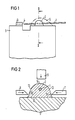
- the example shown in the figures relates to a detail inside a special module for an optical fiber communication system.
- a glass fiber end section e.g. a single-mode glass fiber end section 1, in the optically active direction of an optoelectronic component 3, e.g. a GaAs laser 3, on which - e.g. by means of a PTC thermistor, not shown, touching the temperature-stabilized metal block 5.
- the end section 1 is precisely adjusted to the optically active point 4 of this structure 3.
- cf. 1 a trench can be attached to the block surface 5, which can facilitate precise positioning of the structure 3 in mass production.
- the end section 1 was soldered to a holding body 2 within the protective housing in such a way that the axis of the end section 1 in the active direction, held by the holding body 2, provisionally more or less on the during the soldering active position 4 was aligned.
- the holding body 2 was a solid base 2, which itself consisted of ductile material, namely the solder itself on the metal block 5.
- the base 2 therefore had a very compact, rigid structure, whereby it was mechanically very rigidly connected to the laser 3 on the common metal block 5 - via its base 10 with, for example, 2 mm distance from the laser 3.
- the end section 1 was precisely adjusted to the active point 4 by cold shaping the hardened solder droplet 2, namely by squeezing.
- the holding body 2 ie the solder droplet 2 itself, and not any ductile intermediate part, was deformed in order to achieve the final precise adjustment.
- the arrangement shown according to the invention therefore reacts quite insensitively to temperature fluctuations after its final adjustment, as a result of which there are hardly any temperature-related misalignments of the end section 1.
- the precision of the adjustment of the tip of the end section 1 perpendicular to the axis direction of the end section 1 by squeezing e.g. be adhered to with an accuracy of ⁇ 0.1 ⁇ m, both the production of the base 2 and the squeezing requiring very little effort, that is to say particularly well suited for mass production of such modules.
- this ductile base 2 can be squeezed at the deformation points 11 and / or 12 between the end section, for example 1 and the foot 10 deform, whereby the axis direction is pressed either laterally, with reference to FIG. 2, and / or upwards, that is to say in the direction of point 14. If one squeezes the base 2 on one side, for example, only at the deformation point 12, the axial direction is pressed more laterally, that is to say, for example, in the direction of the point 11 or more upwards, that is to say the point 14, depending on the position of the deformation point.
- the axis device is essentially pushed upwards, that is to say from the foot 10 away to the position 14.
- the warping of the preliminary adjustment set in the first step between the first and the second step is weaker if the base 2 completely surrounds the end section 1, as shown in the figures. Then, in the second step, the base 2 must be deformed less.
- the axis direction can also be pressed downward as desired, that is, in the direction of the foot 10, if the base 2 is deformed on its side 14 facing away from the foot 10, that is to say it is squeezed at the top by means of a stamp 9.
- a largely purely lateral displacement of the axis direction to the left or right is achieved if the base 2 is on the side, cf. the point 13, next to the glass fiber 1 on a more or less perpendicular to the foot 10 facing outer surface 13 of the base 2 squeezes.
- the final adjustment becomes particularly precise if you squeeze the base 2 iteratively several times in succession, i.e. if necessary e.g. iteratively in any order at points 11, 12, 13 and / or 14 until the adjustment is finally optimal, which can be measured by measuring the optical coupling between the structure 3 and the glass fiber 1.
- the finally deformed base 2 can be encased with a hardening protective layer 6 in order to protect the base 2 and thus the adjustment against chemical environmental influences and to stabilize it mechanically.
Landscapes
- Physics & Mathematics (AREA)
- General Physics & Mathematics (AREA)
- Optics & Photonics (AREA)
- Optical Couplings Of Light Guides (AREA)
Applications Claiming Priority (2)
| Application Number | Priority Date | Filing Date | Title |
|---|---|---|---|
| DE3608246 | 1986-03-12 | ||
| DE3608246 | 1986-03-12 |
Publications (1)
| Publication Number | Publication Date |
|---|---|
| EP0241669A1 true EP0241669A1 (fr) | 1987-10-21 |
Family
ID=6296181
Family Applications (1)
| Application Number | Title | Priority Date | Filing Date |
|---|---|---|---|
| EP87102149A Withdrawn EP0241669A1 (fr) | 1986-03-12 | 1987-02-16 | Procédé de fixage et d'alignement d'une pièce terminale d'une fibre de verre |
Country Status (2)
| Country | Link |
|---|---|
| US (1) | US4778241A (fr) |
| EP (1) | EP0241669A1 (fr) |
Cited By (1)
| Publication number | Priority date | Publication date | Assignee | Title |
|---|---|---|---|---|
| GB2230647A (en) * | 1989-04-03 | 1990-10-24 | Tektronix Inc | Electro-optical transducer module and method of fabricating such a module |
Families Citing this family (22)
| Publication number | Priority date | Publication date | Assignee | Title |
|---|---|---|---|---|
| DE3244882A1 (de) * | 1982-12-03 | 1984-06-07 | Siemens AG, 1000 Berlin und 8000 München | Sende- oder empfangsvorrichtung mit einer mittels eines traegers gehalterten diode |
| JPS6043889A (ja) * | 1983-08-22 | 1985-03-08 | Hitachi Ltd | 光ファイバー付レーザーダイオード装置の組立方法 |
| JPH01292875A (ja) * | 1988-05-20 | 1989-11-27 | Oki Electric Ind Co Ltd | 半導体光増幅モジュール |
| FR2672697B1 (fr) * | 1991-02-08 | 1994-06-03 | Alcatel Nv | Dispositif optoelectronique monte sur substrat et connecte par fibre optique, et son procede de fabrication. |
| GB2296101B (en) * | 1994-12-12 | 1998-04-01 | Northern Telecom Ltd | Optically coupling optical fibres to injection lasers |
| US6430337B1 (en) | 1998-09-03 | 2002-08-06 | Agere Systems Optoelectronics Guardian Corp. | Optical alignment system |
| US7003211B2 (en) * | 1999-11-15 | 2006-02-21 | Axsun Technologies, Inc. | Optical system production system |
| US6559464B1 (en) | 1999-11-15 | 2003-05-06 | Axsun Technologies, Inc. | Optical system active alignment process including alignment structure attach, position search, and deformation |
| US6625372B1 (en) | 1999-11-15 | 2003-09-23 | Axsun Technologies, Inc. | Mounting and alignment structures for optical components |
| US6892444B1 (en) * | 2000-09-21 | 2005-05-17 | Axsun Technologies, Inc. | Optical system manufacturing and alignment system |
| US6567604B1 (en) | 2000-10-25 | 2003-05-20 | Omm, Inc. | Indium plated package for an optical component and process therefore |
| EP1306707A1 (fr) * | 2001-10-22 | 2003-05-02 | Agilent Technologies, Inc. (a Delaware corporation) | Procédé d'alignement des composants optiques |
| US7430081B2 (en) * | 2002-02-28 | 2008-09-30 | Emcore Corporation | Sub-micron adjustable mount for supporting a component and method |
| US7126078B2 (en) | 2002-02-28 | 2006-10-24 | Emcore Corporation | Sub-micron adjustable mount for supporting a component and method |
| US7410088B2 (en) * | 2003-09-05 | 2008-08-12 | Matsushita Electric Industrial, Co., Ltd. | Solder preform for low heat stress laser solder attachment |
| US7021838B2 (en) * | 2003-12-16 | 2006-04-04 | Matsushita Electric Industrial Co., Ltd. | Optimizing alignment of an optical fiber to an optical output port |
| US7140783B2 (en) * | 2004-02-06 | 2006-11-28 | Matsushita Electric Industrial Co., Ltd. | Diamond 2D scan for aligning an optical fiber to an optical output port |
| US7263260B2 (en) * | 2005-03-14 | 2007-08-28 | Matsushita Electric Industrial Co., Ltd. | Low cost, high precision multi-point optical component attachment |
| US8477298B2 (en) * | 2009-09-30 | 2013-07-02 | Corning Incorporated | Angle-cleaved optical fibers and methods of making and using same |
| US20110075976A1 (en) * | 2009-09-30 | 2011-03-31 | James Scott Sutherland | Substrates and grippers for optical fiber alignment with optical element(s) and related methods |
| US8295671B2 (en) * | 2009-10-15 | 2012-10-23 | Corning Incorporated | Coated optical fibers and related apparatuses, links, and methods for providing optical attenuation |
| US20160011386A1 (en) * | 2013-03-27 | 2016-01-14 | Ccs Technology, Inc. | Optoelectronic device and method of assembling an optoelectronic device |
Citations (10)
| Publication number | Priority date | Publication date | Assignee | Title |
|---|---|---|---|---|
| US3826998A (en) * | 1970-02-20 | 1974-07-30 | Siemens Ag | Gas laser |
| FR2386919A1 (fr) * | 1977-04-05 | 1978-11-03 | Philips Nv | Procede pour ajuster un element optique d'un laser a decharge dans un gaz et laser a decharge dans un gaz muni d'un element optique ainsi ajuste |
| US4296998A (en) * | 1979-12-17 | 1981-10-27 | Bell Telephone Laboratories, Incorporated | Encapsulated light source with coupled fiberguide |
| EP0050051A1 (fr) * | 1980-09-23 | 1982-04-21 | Thomson-Csf | Procédé d'alignement d'une fibre optique avec un composant opto-électronique, adaptateur, et tête de couplage comportant l'utilisation du procédé |
| EP0112211A1 (fr) * | 1982-11-30 | 1984-06-27 | Thomson-Csf | Procédé d'alignement d'un dispositif optoélectronique |
| DE3430762A1 (de) * | 1983-08-22 | 1985-03-14 | Hitachi Iruma Electronic Co., Ltd., Iruma, Saitama | Licht emittierendes bauelement |
| EP0137485A2 (fr) * | 1983-10-12 | 1985-04-17 | Siemens Aktiengesellschaft | Elément de traversée en fibre de verre dans une ouverture de boîtier |
| DE3405838A1 (de) * | 1984-02-17 | 1985-08-22 | Siemens AG, 1000 Berlin und 8000 München | Verfahren zur zentrierung einer glasfaserspitze |
| DE3411896A1 (de) * | 1984-03-30 | 1985-10-24 | Siemens AG, 1000 Berlin und 8000 München | Anordnung zur optischen anpassung eines lichtwellenleiters |
| DE3431775A1 (de) * | 1984-08-29 | 1986-03-13 | Siemens AG, 1000 Berlin und 8000 München | Anordnung zur justierbaren ausrichtung eines lichtwellenleiters und verfahren zur justierung mit hilfe einer solchen anordnung |
Family Cites Families (7)
| Publication number | Priority date | Publication date | Assignee | Title |
|---|---|---|---|---|
| US4065203A (en) * | 1975-12-10 | 1977-12-27 | International Telephone And Telegraph Corporation | Couplers for electro-optical elements |
| CA1108900A (fr) * | 1978-09-15 | 1981-09-15 | Paul P. Webb | Logement de dispositif electro-opitique pour l'usage dans l'optique des fibres |
| FR2440005A1 (fr) * | 1978-10-27 | 1980-05-23 | Socapex | Embout de connecteur pour monofibre optique, et procede de fixation d'un tel embout sur une telle monofibre |
| JPS5776885A (en) * | 1980-10-31 | 1982-05-14 | Nec Corp | Optical semiconductor device |
| JPS5776510A (en) * | 1980-10-31 | 1982-05-13 | Nec Corp | Light transmitter |
| FR2529349A1 (fr) * | 1982-06-25 | 1983-12-30 | Souriau & Cie | Connecteur de fibre optique pour support coulissant dans une armoire ratelier |
| EP0104882B1 (fr) * | 1982-09-29 | 1986-08-27 | THE GENERAL ELECTRIC COMPANY, p.l.c. | Montages pour le couplage d'une fibre optique |
-
1987
- 1987-02-16 EP EP87102149A patent/EP0241669A1/fr not_active Withdrawn
- 1987-03-09 US US07/023,418 patent/US4778241A/en not_active Expired - Fee Related
Patent Citations (10)
| Publication number | Priority date | Publication date | Assignee | Title |
|---|---|---|---|---|
| US3826998A (en) * | 1970-02-20 | 1974-07-30 | Siemens Ag | Gas laser |
| FR2386919A1 (fr) * | 1977-04-05 | 1978-11-03 | Philips Nv | Procede pour ajuster un element optique d'un laser a decharge dans un gaz et laser a decharge dans un gaz muni d'un element optique ainsi ajuste |
| US4296998A (en) * | 1979-12-17 | 1981-10-27 | Bell Telephone Laboratories, Incorporated | Encapsulated light source with coupled fiberguide |
| EP0050051A1 (fr) * | 1980-09-23 | 1982-04-21 | Thomson-Csf | Procédé d'alignement d'une fibre optique avec un composant opto-électronique, adaptateur, et tête de couplage comportant l'utilisation du procédé |
| EP0112211A1 (fr) * | 1982-11-30 | 1984-06-27 | Thomson-Csf | Procédé d'alignement d'un dispositif optoélectronique |
| DE3430762A1 (de) * | 1983-08-22 | 1985-03-14 | Hitachi Iruma Electronic Co., Ltd., Iruma, Saitama | Licht emittierendes bauelement |
| EP0137485A2 (fr) * | 1983-10-12 | 1985-04-17 | Siemens Aktiengesellschaft | Elément de traversée en fibre de verre dans une ouverture de boîtier |
| DE3405838A1 (de) * | 1984-02-17 | 1985-08-22 | Siemens AG, 1000 Berlin und 8000 München | Verfahren zur zentrierung einer glasfaserspitze |
| DE3411896A1 (de) * | 1984-03-30 | 1985-10-24 | Siemens AG, 1000 Berlin und 8000 München | Anordnung zur optischen anpassung eines lichtwellenleiters |
| DE3431775A1 (de) * | 1984-08-29 | 1986-03-13 | Siemens AG, 1000 Berlin und 8000 München | Anordnung zur justierbaren ausrichtung eines lichtwellenleiters und verfahren zur justierung mit hilfe einer solchen anordnung |
Cited By (2)
| Publication number | Priority date | Publication date | Assignee | Title |
|---|---|---|---|---|
| GB2230647A (en) * | 1989-04-03 | 1990-10-24 | Tektronix Inc | Electro-optical transducer module and method of fabricating such a module |
| GB2230647B (en) * | 1989-04-03 | 1993-02-24 | Tektronix Inc | Electro-optical transducer module and a method of fabricating such a module |
Also Published As
| Publication number | Publication date |
|---|---|
| US4778241A (en) | 1988-10-18 |
Similar Documents
| Publication | Publication Date | Title |
|---|---|---|
| EP0241669A1 (fr) | Procédé de fixage et d'alignement d'une pièce terminale d'une fibre de verre | |
| DE3786900T2 (de) | Optischer Verbinder und dessen Herstellungsverfahren. | |
| DE69429910T2 (de) | Wellenleiter-optische Faser Verbindungsstruktur und Wellenleiter-optische Faser Verbindungsverfahren | |
| DE69535688T2 (de) | Optisches Halbleitermodul und Verfahren zu seiner Herstellung | |
| DE69526563T2 (de) | Optisches Koppeln von Fasern an Injektionslasern | |
| EP0217063B1 (fr) | Dispositif optique | |
| DE3405805A1 (de) | Schutzrohranordnung fuer glasfaser | |
| DE69331876T2 (de) | Ausrichtung von integrierten optischen Komponenten | |
| DE69109231T2 (de) | Ausrichtvorrichtung von einer optischen Faser und von einem optoelektronischen Bauelement. | |
| DE4232608C2 (de) | Verfahren zum Herstellen eines Deckels für eine integriert optische Schaltung | |
| DE69013068T2 (de) | Verbinder für Lichtwellenleiter. | |
| DE69109806T2 (de) | Laserdiodenmodul mit Glasfaserausgang. | |
| DE69624099T2 (de) | Miniatur-haltevorrichtung | |
| DE3138296C2 (fr) | ||
| DE19644758A1 (de) | Zentrieranordnung zum Positionieren von mikrostrukturierten Körpern | |
| DE3021228A1 (de) | Verfahren zur anbringung einer optischen faser an einer halbleiteranordnung | |
| EP0463297A1 (fr) | Dispositif comprenant un substrat et un composant et procédé de fabrication | |
| DE3608018A1 (de) | Verbindungselement fuer mit kleber gehaltene lichtwellenleiter und verfahren zu dessen herstellung | |
| DE3433717C2 (fr) | ||
| DE4240950C1 (de) | Verfahren zum Herstellen eines Deckels für eine integriert optische Schaltung und Deckel für eine integriert optische Schaltung | |
| DE3307669C2 (fr) | ||
| DE102019211077A1 (de) | Elektrisches und/oder elektronisches Bauelement und Kontaktanordnung | |
| EP0515784B1 (fr) | Dispositif pour positionner des fibres optiques | |
| DE102019121924B4 (de) | Laserbaugruppe und zugehörige verfahren | |
| WO2007042385A2 (fr) | Structure optique a suspension elastique, et son procede de production |
Legal Events
| Date | Code | Title | Description |
|---|---|---|---|
| PUAI | Public reference made under article 153(3) epc to a published international application that has entered the european phase |
Free format text: ORIGINAL CODE: 0009012 |
|
| AK | Designated contracting states |
Kind code of ref document: A1 Designated state(s): CH DE FR GB IT LI |
|
| 17P | Request for examination filed |
Effective date: 19871125 |
|
| 17Q | First examination report despatched |
Effective date: 19890728 |
|
| STAA | Information on the status of an ep patent application or granted ep patent |
Free format text: STATUS: THE APPLICATION IS DEEMED TO BE WITHDRAWN |
|
| 18D | Application deemed to be withdrawn |
Effective date: 19891208 |
|
| RIN1 | Information on inventor provided before grant (corrected) |
Inventor name: HALTENORTH, HELMUT, DR. PHYS. |