EP0241783A2 - Système d'interconnexion pour signaux numériques - Google Patents
Système d'interconnexion pour signaux numériques Download PDFInfo
- Publication number
- EP0241783A2 EP0241783A2 EP87104499A EP87104499A EP0241783A2 EP 0241783 A2 EP0241783 A2 EP 0241783A2 EP 87104499 A EP87104499 A EP 87104499A EP 87104499 A EP87104499 A EP 87104499A EP 0241783 A2 EP0241783 A2 EP 0241783A2
- Authority
- EP
- European Patent Office
- Prior art keywords
- bit
- network
- stage
- bits
- input
- Prior art date
- Legal status (The legal status is an assumption and is not a legal conclusion. Google has not performed a legal analysis and makes no representation as to the accuracy of the status listed.)
- Withdrawn
Links
- 238000000034 method Methods 0.000 claims description 16
- 230000001360 synchronised effect Effects 0.000 claims description 13
- 230000001172 regenerating effect Effects 0.000 claims description 4
- 238000012163 sequencing technique Methods 0.000 claims 1
- 230000005540 biological transmission Effects 0.000 description 12
- 230000000903 blocking effect Effects 0.000 description 11
- 241000238876 Acari Species 0.000 description 10
- 230000008569 process Effects 0.000 description 7
- 230000008707 rearrangement Effects 0.000 description 6
- 230000008929 regeneration Effects 0.000 description 6
- 238000011069 regeneration method Methods 0.000 description 6
- 238000006243 chemical reaction Methods 0.000 description 5
- 230000003111 delayed effect Effects 0.000 description 5
- 239000003550 marker Substances 0.000 description 4
- 230000006870 function Effects 0.000 description 3
- 230000000630 rising effect Effects 0.000 description 3
- 230000008901 benefit Effects 0.000 description 2
- 230000001143 conditioned effect Effects 0.000 description 2
- 238000010586 diagram Methods 0.000 description 2
- 230000001902 propagating effect Effects 0.000 description 2
- 230000009467 reduction Effects 0.000 description 2
- 239000004065 semiconductor Substances 0.000 description 2
- 238000004891 communication Methods 0.000 description 1
- 230000003750 conditioning effect Effects 0.000 description 1
- 230000001934 delay Effects 0.000 description 1
- 238000013461 design Methods 0.000 description 1
- 238000005516 engineering process Methods 0.000 description 1
- 238000000605 extraction Methods 0.000 description 1
- 238000009432 framing Methods 0.000 description 1
- 238000012423 maintenance Methods 0.000 description 1
- 239000011159 matrix material Substances 0.000 description 1
- 238000012544 monitoring process Methods 0.000 description 1
- 238000012545 processing Methods 0.000 description 1
- 230000003252 repetitive effect Effects 0.000 description 1
- 230000007704 transition Effects 0.000 description 1
- 238000013024 troubleshooting Methods 0.000 description 1
Images


Classifications
-
- H—ELECTRICITY
- H04—ELECTRIC COMMUNICATION TECHNIQUE
- H04Q—SELECTING
- H04Q11/00—Selecting arrangements for multiplex systems
- H04Q11/04—Selecting arrangements for multiplex systems for time-division multiplexing
Definitions
- This invention relates generally to digital signal cross-connect systems and more particularly to an electronically controlled cross-connect system using a space division switching network to cross-- connect digital signals which may be synchronous or asynchronous to one another.
- a typical node will include a number of transmission terminals which send and receive signals from transmission terminals at other nodes, and an intra-node cross-connect system which routes signals between the transmission terminals at that node.
- a rudimentary cross-connect system is simply an array of jacks providing signal access to transmission terminals and patch cords providing jack-to-jack connections. The rudimentary cross-connect system can be reconfigured by manually rearranging the patch cords.
- the rudimentary cross-connect system is functionally and administratively inadequate for large modern networks with high traffic volume and frequent requirements for circuit re-routing.
- Such networks require large cross-connect systems which can be reconfigured electronically from a local control terminal or remotely from a network control master station.
- An electronic cross-connect system is a switch network which provides electronically switchable paths between its inputs and outputs.
- the signals connected to the cross-connect system are all of the same type.
- the signals are all digital and all at the same nominal bit-rate, although not necessarily synchronous with one another.
- Digital signals can be switched by time division methods, or space division methods, or a combination of both.
- Time division methods use multiplexing of low-bit-rate space-divided signals into higher-bit-rate time-divided signals, followed by time slot interchanges, followed by demultiplexing to lower-bit-rate space divided signals. If the space divided signals to be switched are already at high bit-rates, it may be impractical to multiplex them to higher rates for switching purposes, but high-bit-rate signals can be switched by space division methods.
- This invention relates to space division switching networks for high-bit-rate digital signals, but the principles of the invention are also applicable to low-bit-rate digital signals.
- space division switch networks were developed in terms of electro-mechanical switching machines for low frequency analog signals, wherein metallic crosspoints make or break metallic paths through the network. Such networks are inherently capable of transmission in either direction without signal conditioning, even in very large networks. Such networks are inappropriate for high-bit-rate digital signals.
- High-bit-rate digital signals are more appropriately switched in networks of "large scale integrated" semiconductor devices wherein logic gates provide the crosspoint function.
- Such networks are inherently capable of transmission in one direction only, and the digital signals may require regeneration (i.e., reshaping and retiming) as they traverse the network.
- a well-known class of high capacity space division switching network is the multistage coordinate switching network described by C. Clos in "A Study of Non-Blocking Switching Networks," Bell System Technical Journal, March 1953.
- a Clos network is non-blocking in the sense that a new path can always be connected from any input to any output without changing any of the already-connected internal paths in the network.
- a non-blocking "rearrangeable” network is one in which a new path can always be connected from any input to any output, provided one is allowed to rearrange already-connected internal paths without changing their endpoints.
- the advantage of a rearrangeable network over a Clos network is a major reduction in total number of crosspoints.
- An objects of the present invention is to provide a rearrangeable switching network for high-bit-rate digital signals in which existing through traffic is not disturbed when a new connection is made.
- a high-bit-rate digital signal propagating through a large space division switch may be seriously degraded as it passes through a succession of crosspoints (logic gates) along its path.
- every through signal may require regeneration (reshaping and retiming) at one or more stages within the switch network.
- Digital signal regeneration requires a clock waveform for retiming. If the through signals are all synchronous and bit-aligned to a common clock, then this one clock can be used for all regenerators within the switch network. However, if the through signals are asynchronous, then each one requires its own clock for regeneration.
- Another object of the present invention is to provide a space division switch network with internal signal regeneration for high-bit-rate digital signals which requires only one clock frequency for internal regenerators regardless of whether the through signals are synchronous or asynchronous. This object is acheived by converting asynchronous digital through signals to bit streams which are synchronous within the switch network.
- the present invention is a digital signal cross-connect system comprising a switched network having N input terminals and M output terminals where the switched network provides internal signal paths, each path connecting one input terminal to any one or more of the output terminals.
- the system further includes means for rearranging the internal paths witout changing their end points and without disturbing the digital signals received at the output terminals of the rearranged paths.
- the system includes means for regenerating the digital signals flowing over the internal paths.
- Another aspect of the present invention provides for either synchronous or asynchronous traffic signals through the digital signal cross-connect system.
- the high bit-rate digital signals applied to digital cross-connect systems generally occur in pairs, a "go" signal and a "return” signal, together constituting one two-way digital communication channel.
- a cross-connect system connecting N/2 two-way channels to another N/2 two-way channels can be constructed as two one-way switches, each with N/2 inputs and N/2 outputs.
- the cross-connect can be constructed as one one-way switch with N inputs and N outputs.
- the second arrangement is more flexible in application because it can switch any input to any output, whereas the first arrangement cannot.
- the single NxN switch can "loopback" a two-way channel by connecting the incoming path to the outgoing path.
- the double (N/2)x(N/2) switch cannot, because the incoming and outgoing paths are on separate switches. For this and other reasons, the single NxN switch is preferred, even though it requires more crosspoints. Its input and outputs may be paired to form a total of N two-way ports.
- Fig. 1 is a block diagram of a digital electronic cross-connect system.
- the switched network is a one-way space-division non-blocking NxN switch which connects any of N inputs to any of N outputs.
- the system time base provides various timing waveforms to the network and the interface circuits.
- the network input and output signals are in some suitable switching format, such as unipolar NRZ (non-return to zero), all bit-aligned and bit-rate synchronous to a common system clock.
- the input signals to the input interface circuits and the output signals from the output interface circuits are in some suitable transmission format, such as B3ZS (bipolar, three zeros suppressed) for DS3 signals (level 3 of standard digital signal hierarchy), at some standard nominal bit rate, not necessarily synchronous with one another.
- B3ZS bipolar, three zeros suppressed
- DS3 signals level 3 of standard digital signal hierarchy
- the input and output interface circuits perform the required format and bit rate conversions.
- a very similar conversion function is necessary and widely used in digital signal multiplexing-demultiplexing systems, wherein independent asynchronous input signals are format converted, brought to a common bit rate, and bit-aligned before being multiplexed (by bit interleaving) into a higher bit-rate signal of the digital signal hierarchy.
- the input and output interface circuits of Fig. 1 are very similar to interface circuits described elsewhere in connection with digital multiplexing-demultiplexing systems. There are, however, significant differences which will be discussed subsequently. We will first discuss the switch network.
- a 3-stage Clos network would have the configuration of Fig. 2 where the first stage consists of 1024/n switches, each with n inlets and 2n-l outlets, the second stage consists of 2n-l switches, each with 1024/n inlets and 1024/n outlets, and the third stage consists of 1024/n switches, each with 2n-l inlets and n outlets.
- the stage-to-stage connection pattern in Figs. 2, 3 and 4 is this: output j of switch k is connected to input k of switch j.
- the crosspoint reduction can be carried further by replacing the smaller non-blocking switches of Figs. 2 or 3 by 3-stage equivalents.
- the 32x32 switch for the rearrangeable network can be realized as a 3-stage rearrangeable network, as in Fig. 4, where the first and third stages each consist of eight 4x4 switches, and the second stage consists of four 8x8 switches, for a total of 512 crosspoints versus the 1024 crosspoints in a single stage 32x32 switch.
- This configuration has been chosen as an example because it is consistant with the current capabilities of semiconductor gate array technology.
- the 32x32 switch unit of Fig. 4 can be fabricated as one integrated circuit because it falls comfortably within the current practical limitations on total gates, package pins and power dissipation.
- the I.C. package includes other features described in the following.
- the same 32x32 switch unit (I.C. package) can be used to construct switch networks of smaller and larger capacity than the network of Fig. 3.
- the first and third states each require one switch unit for every 32 inputs.
- N is less than 1024
- the second stage may have 32 switch units, as in Fig. 3.
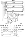
- Each.4x4 switch in Fig. 4 can be realized as an array of logic elements as shown in Fig. 5.
- the arrangement of four 3-input AND gates and one 4- input OR gate and register cells 101 and 102 constitute a 1-of-4 selector with a 2-bit address register which connects one of four inputs to the output according to the 2-bit code stored in the address register.
- Four such selectors with their inputs connected in parallel can connect any input to any output (or any input to two or more outputs). That is, they provide a 4x4 non-blocking switch with an 8-bit address register which determines the crosspoint states.
- Register cells 103 and 104 together with corresponding cells in the other three selectors constitute an 8-bit serial shift register, operated by clock CK2, for entering new configuration data into the switch unit.
- clock waveform CK2 is activated to enter a new 8-bit code into the serial register.
- the new configuration is executed when, subsequently, a pulse applied to the r-terminal transfers the new code into the address register.
- Clock CK2 is completely independent of network clock CK1.
- Each 8x8 switch in Fig. 4 can be realized as a paralleled array of eight l-of-8 selectors, each with a 3-bit address register and a 3-bit serial register.
- the eight serial registers are connected in series to form one 24-bit serial register for entering new configuration data into the switch unit.
- the 8x8 switch could be realized as a 3-stage switch in which the first and third stages are each four 2x2 units and the second stage is two 4x4 units. This alternative does not save crosspoints but may be preferred for other reasons. It requires a 32-bit address register. In the following, we will assume a single stage 8x8 switch.
- each output of the 4x4 switch passes through a register cell clocked by CK1, which is the network clock.
- the 8x8 switch units of Fig. 5 have similar regenerators in each signal output. It is also desirable to regenerate each through signal after traversing external package- to-package connections. Therefore, the gate-array I.C. package includes a regenerator for every input signal. Thus, each through signal is regenerated four times within each 32x32 switch unit.
- Each switch unit in Fig. 4 includes a serial shift register, clocked by CK2, as shown in Fig. 5, for entering new configuration data. All of these can be connected in series to form one serial shift register which, in this case, is 224 cells long. This is done to converse pins on the gate-array I.C. package.
- Fig. 4 the total number of address register cells in the twenty switch units is 224. Assume that a particular 224-bit code is currently stored in the address cells. This code determines the condition of every crosspoint in every switch unit of Fig. 4, i.e., the internal path configuration of the 32x32 switch.
- a "tick” is a positive-going transition (rising edge) of a clock waveform. It causes the output of a clocked register cell to conform to its input. The cell holds that output until the next tick.
- the foregoing sequence of r-ticks can be conveniently generated by propagating a pulse (r-pulse) through the serial shift register (r-register), clocked by CK1, shown at the bottom of Fig. 4.
- the register has four cells corresponding to the four stages of regeneration in the signal paths.
- the r-pulse steps along r-register cells in time coincidence with signal bits stepping through the signal regenerators.
- the first cell of the r-register corresponds to the signal input regenerators, the others correspond to switch stage output regenerators.
- Fig. 7a shows the waveform of network clock CK1.
- the clock ticks are the rising edges of C K l Figs. 7d, 7e and 7f show the r-pulse as it appears at successive stages of the r-register.
- the r-ticks are the rising edge of the pulse.
- the length of the pulse is immaterial, because its falling edge does not initiate any circuit actions.
- the signal bits at the 32 inputs of the first stage switches of Fig. 4 be al, a2,....a32 before tl and bl, b2,....b32 after tl.
- the bits at the inputs of the regenerators of the first stage switches are a-bits in a pattern determined by the 64 (old) code bits in the first stage address registers. After tl, these a-bits appear at the inputs of the second stage switches, and the b-bits appear at the inputs of the first stage switches. But rl coincides with tl. rl loads new code bits into the first stage address registers.
- the bits at the inputs of the regenerators of the first stage switches are b-bits in a pattern determined by the 64 new code bits in the first stage address register.
- the bits at the inputs of the regenerators of the second stage switches are a-bits in a pattern determined by the 96 (old) code bits in the second stage address register. After t2, these a-bits appear at the inputs of the third stage switches, and the b-bits appear at the inputs of the second stage switches. But r2 coincides with t2, and r2 leads new code bits into the second stage address registers.
- the bits as the inputs of the regenerators of the second stage switches are b-bits in a pattern determined by the 96 new code bits in the second stage address register.
- the bits at the inputs of the regenerators of the third stage switches are a-bits in a pattern determined by the 64 (old) code bits in the third stage address register. After t3 these a-bits appear at the outputs of the regenerators of the third stage switches, and the b-bits appear at the inputs of the third stage switches. But r3 coincides with t3..r3 leads new code bits into the third stage address registers. Therefore, after t3 the bits at the input of the regenerators of the third stage switches are b-bits in a pattern determined by the 64 new code bits in the third stage address register. It can hence be seen how the process continues with subsequent cycles.
- Fig. 3 is a 3-stage network of 3-stage networks, i.e., a 9- stage network, which can be reconfigured in a nine- step sequence as described above.
- the r-register outputs of first stage switch units are connected to r-register inputs of second stage switch units and the r-register outputs of second stage switch units are connected to r-register inputs of third stage switch units.
- These connections yield a 12-stage shift register which generates three sets of three r-ticks with a one-tick delay between sets. The three one-tick delays accommodate the input regenerators in the 32x32 switches.
- any input may be connected to one or more outputs.
- each 32x32 switch package with a 33rd output terminal plus internal circuitry to bridge the 33rd terminal onto any other output.
- the internal circuitry is a l-of-32 selector which can be realized in several ways; e.g., eight l-of-24 selectors (with the same 2-bit address) followed by one l-of-8 selector (with 3-bit address), the combination requiring five address register cells to select the desired signal output.
- the bridging address register and its clock should preferably be completely separate from the serial register and clock (CK2) used for loading switch configuration codes. The bridging address input and clock require two more pins on the I.C. package.
- the switch network input signals were in NRZ format, all bit-aligned and all bit-rate synchronous to a common network clock CKl.
- the signal inputs to the input interface circuits will generally be in transmission format, not bit-aligned, and probably not synchronous.
- the input interface circuits provide the necessary conversion in signal characteristics. They are similar to interface circuits described elsewhere in connection with digital signal multiplexer-demultiplexer systems.
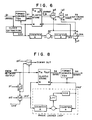
- Fig. 6 shows essential elements of the input interface circuit.
- the input signal Sl will be in a format which carries "embedded clock," such as B3ZS for DS3 signals.
- the clock extraction circuit derives a continuous clock waveform CKS from the input signal.
- CKS is used for regenerating Sl, for timing the format conversion of Sl from B3ZS to NRZ, and for writing Sl bits (data bits) into a small FIFO '(first in, first out) memory commonly known as an “elastic store” or “timing buffer;”
- the data bits are read out of the memory by a different clock, CK3, which is derived from the network clock C K 1 which operates the internal regenerators within the switch network, as already described above.
- the memory output is connected directly to the switch network input, and clock CK1 is used to clock bits out of the elastic store.
- the elastic store serves only to absorb differential input jitter and provide bit alignment at the network input.
- the many input signals are asynchronous. They are individually brought to a common bit rate by a process commonly known as "bit-stuffing".
- network clock CK1 is slightly greater (typically less than 1% greater) than the nominal bit rate of the input signals.
- Each frame may contain 98 or 99 data bits, so over many frames the average number of data bits per frame can be any number between 98 and 99.
- any input signal bit rate lies between 98% and 99% of the network clock rate (CKl)
- that input signal can be re-written as a "stuffed" bit stream (S2 in Fig. 6) at CK1 rate.
- the stuffed bit stream contains all of the bits from Sl plus overhead in the form of m-bits (one per frame) and dummy bits (none or one per frame) at known locations in the frame.
- a subsequent "destuffing" operation will remove the overhead bits and re-write the data bits onto a bit stream at the clock rate of the original input signal.
- bit-stuffing multiplexer applications it is customary to provide redundant m-bits so that the marker value can be error protected. Note that the stuffed bit stream does not include a framing code to locate the marker bits. There is no need for the marker bits and maybe bits to be adjacent to one another.
- the mechanics of bit stuffing are indicated in Figs. 6 and 7.
- the network clock CK1 provides 100 "ticks" per frame (Fig. 7a).
- CK4 is the same clock with every tick #1 removed (Fig. 7b).
- CK 3 is derived from CK4 by sometimes removing tick #2.
- pl and p2 are timing pulses which occur once per frame, coincident with ticks #1 and #2.
- CKS clocks data bits (from Sl) into the elastic store and drives counter B. Counts A and B are compared. If count B exceeds count A, logic L2, timed by p2, removes tick #2 from CK3 (Fig. 7c), which retards count B relative to count A. This process forces count B to follow count A. Therefore, CK3 and CKS have the same average number of ticks and data bits are clocked out of the elastic store by CK3 at the same average rate they are clocked in by CKS. The store does not overflow or underflow. No data is lost.
- the elastic store provides new data on ticks #3 and through #100. It provides no data on tick #1.
- All input interface circuits use the same pl, p2 and CK4 generated in the system time base.
- Each input interface circuit generates its own CK3, which depends on CKS.
- the inputs to the switched network are the independently stuffed bit streams, all synchronized to network clock CK1.
- the outputs of the switched network are the independently stuffed bit streams rearranged according to the network I-O map, and all equally delayed by an integral number of time slots equal to the number of regenerators in a switch path.
- Fig. 8 shows the principal elements of the output interface circuit, wherein the switch network output signal S3 is "destuffed” and reformatted as signal S4, for ongoing transmission. Let the transit time through the switch be d time slots. Then S3 is a replica of S2, delayed by d time slots, pl, p2 and CK4 are replicas of pl, p2 and CK4 (of Fig. 6) delayed by d time slots. All output interface circuits use the same pl', p2' and CK4' generated in the system time base.
- pl' and the missing ticks of CK4' coincide with m-bits in S3.
- logic Ll, timed by pl registers the value of the m-bit.
- CK3' is used as write clock for the elastic store in Fig. 8.
- the missing ticks of CK3' coincide with the m-bits and the dummy bits in S3. Therefore, these bits are not written. Only the data bits in S3 are clocked into the store.
- CK3' is also used as input to a phase locked loop which generates clock waveform CKS' which clocks data out of the elastic store.
- the phase locked loop is a conventional configuration of voltage controlled oscillator (VCO), two counters, a difference circuit, and a low pass filter (LPF).
- VCO voltage controlled oscillator
- LPF low pass filter
- CKS' has the same number of ticks as CK3', but they are uniformly distributed in time - except for a small amount of low frequency jitter which is an inevitable consequence of the stuff/destuff processing.
- CKS' has precisely the same average bit rate as CKS, but CKS' is not a delayed version replica of CKS. In particular, the stuff/destuff process will absorb high frequency jitter components of Sl and not reproduce them in S4.
- CKS' Data bits are clocked out of the elastic store by CKS' at the same average rate they are clocked in by CK3'.
- the store does not overflow or underflow. No data is lost. Therefore, the bits in output signal S4 are identical to the bits in input signal Sl of Fig. 6.
- CKS' also clocks the format conversion logic which coverts the destuffed NRZ signal to B3ZS format. The operations described above are performed individually in every output interface circuit.
- Figs. 6 and 8 include optional logic whereby the dummy bits of the stuffed bit stream can be independently coded at the input interface circuit and extracted at the output interface circuit. This is certainly not necessary but may be advantageous for administrative reasons.
- the dummy bits constitute an independent service channel within each stuffed bit stream.
- the bit rate of the dummy channel depends on the bit rate of the input signal Sl.
- the dummy channels are useful for various administrative or maintenance or monitoring purposes. For example, if dummies are coded in a unique pattern (e.g., alternating) at the input, then pattern violations detected at the output indicate errors in transit along that switch path. In- service path tracing could be accomplished by uniquely coding (e.g., all l's) the dummies at one input and detecting which output receives the unique code.
- every stuffed bit stream has had a dummy bit inserted and removed, but the process has not relied on the value of the coincident m-bit. It makes no difference whether the m-bit was 0 or 1. Therefore, the m-bit can be mutilated within the switch. Furthermore, if m-bits and dummies are contiguous, two consecutive bits can be mutilated without disturbing data bits (through traffic). This procedure could conceivably require a miniscule increase in CK1 clock rate to accommodate the extra dummies created by switch rearrangements. In extreme cases, one could design the switch control system to use multi-bit m-words and thereby allow rearrangements to mutilate several consecutive bits.
- the present invention has been described to illustrate one preferred embodiment of an improved digital cross-connect system where the number of inputs is equal to the number of outputs (N inputs and N outputs).
- N inputs and N outputs are possible, where the number of inputs is not necessarily equal to the number of outputs (e.g., N inputs and M outputs, where N is not necessarily equal to M).
- N inputs and M outputs are not necessarily equal to M.
- N inputs and M outputs where N is not necessarily equal to M.
- the addition of a fifth logic block to Figure 5 provides a switch with four inputs and five outputs in which any output can be connected to any input. Therefore, it is intended that the scope of the present invention be defined by the following claims.
Landscapes
- Engineering & Computer Science (AREA)
- Computer Networks & Wireless Communication (AREA)
- Use Of Switch Circuits For Exchanges And Methods Of Control Of Multiplex Exchanges (AREA)
- Time-Division Multiplex Systems (AREA)
Applications Claiming Priority (2)
| Application Number | Priority Date | Filing Date | Title |
|---|---|---|---|
| US846910 | 1986-03-31 | ||
| US06/846,910 US4804956A (en) | 1986-03-31 | 1986-03-31 | Rearrangeable digital signal space division switching system |
Publications (2)
| Publication Number | Publication Date |
|---|---|
| EP0241783A2 true EP0241783A2 (fr) | 1987-10-21 |
| EP0241783A3 EP0241783A3 (fr) | 1989-02-01 |
Family
ID=25299284
Family Applications (1)
| Application Number | Title | Priority Date | Filing Date |
|---|---|---|---|
| EP87104499A Withdrawn EP0241783A3 (fr) | 1986-03-31 | 1987-03-26 | Système d'interconnexion pour signaux numériques |
Country Status (4)
| Country | Link |
|---|---|
| US (1) | US4804956A (fr) |
| EP (1) | EP0241783A3 (fr) |
| JP (1) | JPS62237897A (fr) |
| CA (1) | CA1272279A (fr) |
Cited By (3)
| Publication number | Priority date | Publication date | Assignee | Title |
|---|---|---|---|---|
| GB2224415A (en) * | 1988-10-31 | 1990-05-02 | Stc Plc | Transmission networks |
| EP0447462A4 (en) * | 1988-12-09 | 1992-11-04 | Transwitch Corporation | Switch components and multiple data rate non-blocking switch network utilizing the same |
| US6693902B1 (en) | 1992-04-23 | 2004-02-17 | Marconi Uk Intellectual Property Ltd. | Cross-connection architecture for SDH signals comprising time-and-space division switch groups |
Families Citing this family (15)
| Publication number | Priority date | Publication date | Assignee | Title |
|---|---|---|---|---|
| US5189406A (en) * | 1986-09-20 | 1993-02-23 | Thorn Emi Plc | Display device |
| US5146477A (en) * | 1987-03-17 | 1992-09-08 | Antonio Cantoni | Jitter control in digital communication links |
| US5072217A (en) * | 1989-10-31 | 1991-12-10 | International Business Machines Corporation | One-sided crosspoint switch with distributed control |
| US5179551A (en) * | 1991-04-08 | 1993-01-12 | Washington University | Non-blocking multi-cast switching system |
| WO1993007691A1 (fr) * | 1991-10-01 | 1993-04-15 | Norand Corporation | Reseau local a radiofrequences |
| US5221498A (en) * | 1991-07-22 | 1993-06-22 | Betz Laboratories, Inc. | Methods and compositions for inhibitoring polymerization of vinyl monomers |
| FI90706C (fi) * | 1992-04-23 | 1994-03-10 | Nokia Telecommunications Oy | Menetelmä ristikytkentämatriisin virheetöntä vaihtamista varten |
| GB2304255B (en) * | 1995-08-07 | 2000-04-12 | Be Aerospace Inc | Multi-stage switch |
| JP3056083B2 (ja) * | 1996-08-15 | 2000-06-26 | 静岡日本電気株式会社 | 無線選択呼出受信機 |
| US6157638A (en) * | 1998-03-23 | 2000-12-05 | Motorola, Inc. | High density packet switch with high speed interfaces and method for using same |
| US6600741B1 (en) * | 1999-03-25 | 2003-07-29 | Lucent Technologies Inc. | Large combined broadband and narrowband switch |
| US6970455B2 (en) * | 1998-11-13 | 2005-11-29 | Lucent Technologies Inc. | Space/time switch architecture |
| US6587461B1 (en) | 1999-06-08 | 2003-07-01 | Cisco Technology, Inc. | TDM switching system and ASIC device |
| CA2283953C (fr) * | 1999-09-27 | 2009-07-28 | Nortel Networks Corporation | Commutateur compact a grande capacite |
| US10934987B2 (en) * | 2017-11-24 | 2021-03-02 | Bezalel Hirsch | Remote starter adapter for use with a communication device |
Family Cites Families (16)
| Publication number | Priority date | Publication date | Assignee | Title |
|---|---|---|---|---|
| NL284712A (fr) * | 1961-11-24 | |||
| US4005272A (en) * | 1974-08-14 | 1977-01-25 | Arthur A. Collins, Inc. | Time folded TST (time space time) switch |
| SE381548B (sv) * | 1974-12-20 | 1975-12-08 | Ellemtel Utvecklings Ab | Anordning for omstyrning av veljarnet |
| US4038497A (en) * | 1975-05-12 | 1977-07-26 | Collins Arthur A | Hardwired marker for time folded tst switch with distributed control logic and automatic path finding, set up and release |
| US4075608A (en) * | 1976-01-19 | 1978-02-21 | The United States Of America As Represented By The Secretary Of The Navy | Multiple-channel data switch |
| US4038638A (en) * | 1976-06-01 | 1977-07-26 | Bell Telephone Laboratories, Incorporated | Efficient rearrangeable multistage switching networks |
| GB1582583A (en) * | 1977-04-05 | 1981-01-14 | Gen Electric Co Ltd | Digital switching arrangements for stored programme control telecommunications systems |
| US4229624A (en) * | 1978-12-21 | 1980-10-21 | Bell Telephone Laboratories, Incorporated | Switching network control arrangement |
| US4317193A (en) * | 1980-02-04 | 1982-02-23 | Bell Telephone Laboratories, Incorporated | Time division nodal switching network |
| US4345116A (en) * | 1980-12-31 | 1982-08-17 | Bell Telephone Laboratories, Incorporated | Dynamic, non-hierarchical arrangement for routing traffic |
| US4417244A (en) * | 1981-09-01 | 1983-11-22 | International Business Machines Corp. | Automatic path rearrangement for blocking switching matrix |
| US4417245A (en) * | 1981-09-02 | 1983-11-22 | International Business Machines Corp. | Digital space division exchange |
| NL8104358A (nl) * | 1981-09-22 | 1983-04-18 | Nederlanden Staat | Werkwijze en inrichting voor het besturen van een schakelnetwerk. |
| US4566007A (en) * | 1983-05-16 | 1986-01-21 | At&T Bell Laboratories | Rearrangeable multiconnection switching networks |
| FR2562368B1 (fr) * | 1984-04-02 | 1989-07-28 | Cit Alcatel | Reseau de connexion spatial pour signaux numeriques a haut debit |
| US4654842A (en) * | 1984-08-02 | 1987-03-31 | Coraluppi Giorgio L | Rearrangeable full availability multistage switching network with redundant conductors |
-
1986
- 1986-03-31 US US06/846,910 patent/US4804956A/en not_active Expired - Lifetime
-
1987
- 1987-03-03 CA CA000531023A patent/CA1272279A/fr not_active Expired
- 1987-03-26 EP EP87104499A patent/EP0241783A3/fr not_active Withdrawn
- 1987-03-30 JP JP62077384A patent/JPS62237897A/ja active Pending
Cited By (3)
| Publication number | Priority date | Publication date | Assignee | Title |
|---|---|---|---|---|
| GB2224415A (en) * | 1988-10-31 | 1990-05-02 | Stc Plc | Transmission networks |
| EP0447462A4 (en) * | 1988-12-09 | 1992-11-04 | Transwitch Corporation | Switch components and multiple data rate non-blocking switch network utilizing the same |
| US6693902B1 (en) | 1992-04-23 | 2004-02-17 | Marconi Uk Intellectual Property Ltd. | Cross-connection architecture for SDH signals comprising time-and-space division switch groups |
Also Published As
| Publication number | Publication date |
|---|---|
| US4804956A (en) | 1989-02-14 |
| EP0241783A3 (fr) | 1989-02-01 |
| CA1272279A (fr) | 1990-07-31 |
| JPS62237897A (ja) | 1987-10-17 |
Similar Documents
| Publication | Publication Date | Title |
|---|---|---|
| US4804956A (en) | Rearrangeable digital signal space division switching system | |
| US4716561A (en) | Digital transmission including add/drop module | |
| US5140611A (en) | Pulse width modulated self-clocking and self-synchronizing data transmission and method for a telephonic communication network switching system | |
| US6879603B1 (en) | Processor-based voice and data time slot interchange system | |
| US5197062A (en) | Method and system for simultaneous analysis of multiplexed channels | |
| US5784369A (en) | Methods and system for switching time-division-multiplexed digital signals of different rates | |
| GB2074815A (en) | Telecommunications switching network using digital switching modules | |
| US5014268A (en) | Parallel time slot interchanger matrix and switch block module for use therewith | |
| US3851105A (en) | Time division switching network employing space division stages | |
| US7301941B2 (en) | Multistage digital cross connect with synchronized configuration switching | |
| US6870838B2 (en) | Multistage digital cross connect with integral frame timing | |
| CA2445001C (fr) | Architectures pour commande electrique de groupage de trafic en une phase | |
| US3740483A (en) | Time division switching system with bilateral time slot interchangers | |
| US4179587A (en) | Bit switching of word formatted data | |
| US7260092B2 (en) | Time slot interchanger | |
| US3637941A (en) | Integrated switching and transmission network for pulse code modulated signals | |
| US4905228A (en) | Digital transmission channel framing | |
| US4924459A (en) | Digital transmission interconnect signal | |
| US4101737A (en) | Control arrangement in a time-space-time (t-s-t) time division multiple (t.d.m.) telecommunication switching system | |
| JPH02192343A (ja) | 時分割多重情報の再配列装置 | |
| NZ194611A (en) | Channel zero switching arrangements for digital telecom exchanges | |
| US4399534A (en) | Dual rail time and control unit for a duplex T-S-T-digital switching system | |
| US3824543A (en) | Digital data interchange circuit for a multiplexer/demultiplexer | |
| GB2085264A (en) | Digital concentrator | |
| US4399369A (en) | Dual rail time and control unit for a duplex T-S-T-digital switching system |
Legal Events
| Date | Code | Title | Description |
|---|---|---|---|
| PUAI | Public reference made under article 153(3) epc to a published international application that has entered the european phase |
Free format text: ORIGINAL CODE: 0009012 |
|
| AK | Designated contracting states |
Kind code of ref document: A2 Designated state(s): DE GB SE |
|
| PUAL | Search report despatched |
Free format text: ORIGINAL CODE: 0009013 |
|
| AK | Designated contracting states |
Kind code of ref document: A3 Designated state(s): DE GB SE |
|
| 17P | Request for examination filed |
Effective date: 19890729 |
|
| 17Q | First examination report despatched |
Effective date: 19910902 |
|
| STAA | Information on the status of an ep patent application or granted ep patent |
Free format text: STATUS: THE APPLICATION IS DEEMED TO BE WITHDRAWN |
|
| 18D | Application deemed to be withdrawn |
Effective date: 19921118 |
|
| RIN1 | Information on inventor provided before grant (corrected) |
Inventor name: BOXALL, FRANK S. |