EP0241956A1 - Halbleitervorrichtung für das Erzeugen eines elektrischen Stromes - Google Patents
Halbleitervorrichtung für das Erzeugen eines elektrischen Stromes Download PDFInfo
- Publication number
- EP0241956A1 EP0241956A1 EP87200368A EP87200368A EP0241956A1 EP 0241956 A1 EP0241956 A1 EP 0241956A1 EP 87200368 A EP87200368 A EP 87200368A EP 87200368 A EP87200368 A EP 87200368A EP 0241956 A1 EP0241956 A1 EP 0241956A1
- Authority
- EP
- European Patent Office
- Prior art keywords
- region
- semiconductor
- type
- semiconductor device
- electron beam
- Prior art date
- Legal status (The legal status is an assumption and is not a legal conclusion. Google has not performed a legal analysis and makes no representation as to the accuracy of the status listed.)
- Withdrawn
Links
Images
Classifications
-
- H—ELECTRICITY
- H01—ELECTRIC ELEMENTS
- H01J—ELECTRIC DISCHARGE TUBES OR DISCHARGE LAMPS
- H01J3/00—Details of electron-optical or ion-optical arrangements common to two or more basic types of discharge tubes or lamps
- H01J3/02—Electron guns
- H01J3/021—Electron guns using a field emission, photo emission, or secondary emission electron source
-
- H—ELECTRICITY
- H01—ELECTRIC ELEMENTS
- H01J—ELECTRIC DISCHARGE TUBES OR DISCHARGE LAMPS
- H01J1/00—Details of electrodes, of magnetic control means, of screens, or of the mounting or spacing thereof, common to two or more basic types of discharge tubes or lamps
- H01J1/02—Main electrodes
- H01J1/30—Cold cathodes, e.g. field-emissive cathode
- H01J1/308—Semiconductor cathodes, e.g. cathodes with PN junction layers
Definitions
- the invention relates to a semiconductor device for generating an electron current, comprising a cathode having a semiconductor body with an n-type surface regio ⁇ and a p-type region in which electrons leaving the semiconductor body can be generated in said body by giving the n-type surface region a positive bias with respect to the p-type region.
- the invention also relates to a pick-up tube and a display device provided with such a semiconductor device.
- thermionic cathodes are used, inter alia, in cathode ray tubes in which they replace the conventional thermionic cathode in which electron emission is generated by heating. In addition they are used in, for example, apparatus for electron microscopy. In addition to the high energy consumption for the purpose of heating, thermionic cathodes have the drawback that they are not immediately ready for operation because they have to be heated sufficiently before emission occurs. Moreover, the cathode material is lost in the long run due to evaporation, so that these cathodes have a limited lifetime.
- the cold cathodes known from the said patent application are based on the emission of electrons from the semiconductor body when a pn-junction is operated in the reverse direction in such a manner that avalanche multiplication occurs. Some electrons may then obtain as much kenetic energy as is required to exceed the electron work function; these electrons are then liberated on the surface and thus supply an electron current.
- the aim is to have a maximum possible efficiency, which can be achieved by a minimum possible work function for the electrons.
- the latter is realised, for example, by providing a layer of material on the surface of the cathode, which decreases the work function.
- Cesium is preferably used for this purpose because it produces a maximum decrease of the electron work function.
- cesium may have drawbacks.
- cesium is very sensitive to the presence(in its ambience) of oxidising gases (water vapour, oxygen, C0 2 ).
- cesium is fairly volatile which may be detrimental in those uses in which substrates or compounds are present in the vicinity of the cathode such as may be the case, for example, in electron lithography or electron microscopy. The evaporated cesium may then precipitate on the said objects.
- a semiconductor device is to this end characterized in that a substantially intrinsic semiconductor region is present between the n-type surface region and the p-type region, the band gap of the intrinsic semiconductor material at the area of the transition between the intrinsic semiconductor material and the p-type region being smaller than that at the area of the transition between the intrinsic semiconductor material and the n-type surface region.
- the band gap By choosing the band gap to be sufficiently small, notably at the transition between the p-type region and the intrinsic material, electrons can tunnel from the valence band to the conduction band with a sufficiently strong electric field. These electrons have a sufficient potential energy to exceed the work function. Since the band gap at the surface is greater, the tunnel effect hardly occurs there (and therefore hardly any electron generation). This is notably achieved in that the intrinsic semiconductor material consists of at least two different semiconductor materials having a different band gap.
- Substantially intrinsic is to be understood to mean in this Application a region having a light p-type or n-type doping with an impurity concentration of not more than 5'10 atoms/cubic cm.
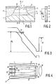
- Figure 1 shows in a cross-section a semiconductor device according to the invention adapted to generate an electron beam.
- this device comprises a cathode having a semiconductor body 1.
- the semiconductor body 1 has at a main surface 2 an n + -type surface region 3 with a thickness of approximately 15 nanometers which is separated from a p +- type substrate 4 by a substantially intrinsic semiconductor layer.
- the substantially intrinsic semiconductor layer is divided into sublayers 5 and 6 with thicknesses of approximately 25 nanometers and approximately 5 nanometers, respectively.
- GaAs gallium arsenide
- Figure 2 diagrammatically shows a cross-section taken on the line II-II in Figure 1, whilst Figure 3 shows the associated electron energy diagram if a voltage of the order of V d is applied across the contacts 8, 9 (see Figure 1) via a voltage source 12, whilst the surface region 3 is positively biased with respect to the substrate 4.
- the voltage V is sufficiently high to generate a field strength in the intrinsic part 5, 6 with a sufficiently high value (for example ⁇ 10 6 V/cm) so that in the GaAs region 6 electrons reach the conduction band from the valence band by means of tunnelling (denoted by arrows 13 in Figure 3). Since the tunnel current density considerably decreases at larger values of the band gap of the semiconductor material, such a tunnel current will substantially only be produced in the GaAs region 6.
- the potential energy of the electrons in the region 6 is greater than the electron emission energy ⁇ .
- the energy difference with respect to ⁇ is such that after a possible energy loss due to interactions with the grid a considerable part of the electrons has sufficient energy to be able to be emitted from the semiconductor body.
- the device of Figure 1 may be manufactured as follows.
- a (100)-oriented p + -substrate of gallium arsenide is initially made which is doped with zinc and has an impurity concentration of approximately 2.10 19 atoms/cm 3 .
- the substantially intrinsic layer likewise of gallium arsenide is successively provided thereon with a thickness of approximately 5 nanometers.
- the Al x Ga 1 -x As layer is provided thereon with a thickness of approximately 25 nanometers.
- the layers 5 and 6 may be lightly doped (JT- or]-type) up to a maximum impurity concentration of 10 16 atoms/cm J , but preferably much less.
- the n +- type surface region 3 is also provided by epitaxial deposition techniques with a thickness of approximately 15 nanometers and an impurity concentration of approximately 4.10 19 atoms/cm 3 .
- the semiconductor material is rendered electrically inactive at the area of the regions 11 as far as the substrate 4, whereafter the assembly is provided with connection contacts 8 and 9.
- the connection contact 8 the device may alternatively be provided with an insulating layer, for example, an oxide layer with an aperture across which conductors extend for the purpose of connection. In that case the electrically inactive region 13 may be dispensed with, if desired.
- cavities may be etched at these areas which are then filled up with oxide, if necessary, until a flat surface is obtained across which connection conductors 8 can extend.
- the device can be provided at the surface 2 within the aperture 10 with a layer of work-function decreasing material such as barium or cesium.
- FIG 4 diagrammatically shows a pick-up tube 21 provided with a semiconductor cathode 1 according to the invention.
- the pick-up tube also comprises a photo- conducting target plate 24 in a hermetically closed vacuum tube 23, which plate is scanned by the electron beam 7, whilst the pick-up tube is also provided with a system of coils 27 for deflecting the beams and with a screen grid 29.
- An image to be picked up is projected onto the target plate 24 with the aid of the lens 28, the end wall 22 being permeable to radiation.
- the end wall 25 is provided with lead-throughs 26.
- the semiconductor cathode according to Figure 1 is mounted on the end wall 25 of the pick-up tube 21.
- a display tube can be realized in which, inter alia, a fluorescent screen is present at the area of end wall 22.
- a number of structures according to Figure 1 may be arranged in a matrix in which the p -substrate 4 is replaced by p + -type zones arranged in rows which constitute row connections and which are then contacted at the surface of the semiconductor body, whilst column connections are realized via parallel arranged connection pins 8.
- the variation of the band gap of the intrinsic semiconductor material may alternatively be obtained by using Al xGa x As where x slowly increases in the direction towards the surface.
- the use of more than two types of semiconductor material is also possible.
- materials of the A 2 B 6 type may alternatively be chosen.
Landscapes
- Cold Cathode And The Manufacture (AREA)
- Cathode-Ray Tubes And Fluorescent Screens For Display (AREA)
- Electrodes For Cathode-Ray Tubes (AREA)
- Image-Pickup Tubes, Image-Amplification Tubes, And Storage Tubes (AREA)
Applications Claiming Priority (2)
| Application Number | Priority Date | Filing Date | Title |
|---|---|---|---|
| NL8600676A NL8600676A (nl) | 1986-03-17 | 1986-03-17 | Halfgeleiderinrichting voor het opwekken van een elektronenstroom. |
| NL8600676 | 1986-03-17 |
Publications (1)
| Publication Number | Publication Date |
|---|---|
| EP0241956A1 true EP0241956A1 (de) | 1987-10-21 |
Family
ID=19847724
Family Applications (1)
| Application Number | Title | Priority Date | Filing Date |
|---|---|---|---|
| EP87200368A Withdrawn EP0241956A1 (de) | 1986-03-17 | 1987-03-02 | Halbleitervorrichtung für das Erzeugen eines elektrischen Stromes |
Country Status (6)
| Country | Link |
|---|---|
| US (1) | US4853754A (de) |
| EP (1) | EP0241956A1 (de) |
| JP (1) | JPS62229731A (de) |
| KR (1) | KR870009482A (de) |
| CA (1) | CA1253260A (de) |
| NL (1) | NL8600676A (de) |
Cited By (2)
| Publication number | Priority date | Publication date | Assignee | Title |
|---|---|---|---|---|
| EP0404246A1 (de) * | 1989-06-23 | 1990-12-27 | Koninklijke Philips Electronics N.V. | Halbleiteranordnung zum Erzeugen eines Elektronenstromes |
| WO1998037567A1 (en) * | 1997-02-24 | 1998-08-27 | Koninklijke Philips Electronics N.V. | Electron tube having a semiconductor cathode |
Families Citing this family (5)
| Publication number | Priority date | Publication date | Assignee | Title |
|---|---|---|---|---|
| US5267884A (en) * | 1990-01-29 | 1993-12-07 | Mitsubishi Denki Kabushiki Kaisha | Microminiature vacuum tube and production method |
| JP2968014B2 (ja) * | 1990-01-29 | 1999-10-25 | 三菱電機株式会社 | 微小真空管及びその製造方法 |
| US5359257A (en) * | 1990-12-03 | 1994-10-25 | Bunch Kyle J | Ballistic electron, solid state cathode |
| US5686789A (en) * | 1995-03-14 | 1997-11-11 | Osram Sylvania Inc. | Discharge device having cathode with micro hollow array |
| US5712490A (en) * | 1996-11-21 | 1998-01-27 | Itt Industries, Inc. | Ramp cathode structures for vacuum emission |
Citations (4)
| Publication number | Priority date | Publication date | Assignee | Title |
|---|---|---|---|---|
| GB1303659A (de) * | 1969-11-12 | 1973-01-17 | ||
| FR2235496A1 (de) * | 1973-06-28 | 1975-01-24 | Hamamatsu Tv Co Ltd | |
| US4040080A (en) * | 1976-03-22 | 1977-08-02 | Hamamatsu Terebi Kabushiki Kaisha | Semiconductor cold electron emission device |
| US4303930A (en) * | 1979-07-13 | 1981-12-01 | U.S. Philips Corporation | Semiconductor device for generating an electron beam and method of manufacturing same |
Family Cites Families (1)
| Publication number | Priority date | Publication date | Assignee | Title |
|---|---|---|---|---|
| US3466512A (en) * | 1967-05-29 | 1969-09-09 | Bell Telephone Labor Inc | Impact avalanche transit time diodes with heterojunction structure |
-
1986
- 1986-03-17 NL NL8600676A patent/NL8600676A/nl not_active Application Discontinuation
-
1987
- 1987-03-02 EP EP87200368A patent/EP0241956A1/de not_active Withdrawn
- 1987-03-05 US US07/021,938 patent/US4853754A/en not_active Expired - Fee Related
- 1987-03-12 CA CA000531875A patent/CA1253260A/en not_active Expired
- 1987-03-14 KR KR870002309A patent/KR870009482A/ko not_active Withdrawn
- 1987-03-16 JP JP62059089A patent/JPS62229731A/ja active Pending
Patent Citations (4)
| Publication number | Priority date | Publication date | Assignee | Title |
|---|---|---|---|---|
| GB1303659A (de) * | 1969-11-12 | 1973-01-17 | ||
| FR2235496A1 (de) * | 1973-06-28 | 1975-01-24 | Hamamatsu Tv Co Ltd | |
| US4040080A (en) * | 1976-03-22 | 1977-08-02 | Hamamatsu Terebi Kabushiki Kaisha | Semiconductor cold electron emission device |
| US4303930A (en) * | 1979-07-13 | 1981-12-01 | U.S. Philips Corporation | Semiconductor device for generating an electron beam and method of manufacturing same |
Cited By (2)
| Publication number | Priority date | Publication date | Assignee | Title |
|---|---|---|---|---|
| EP0404246A1 (de) * | 1989-06-23 | 1990-12-27 | Koninklijke Philips Electronics N.V. | Halbleiteranordnung zum Erzeugen eines Elektronenstromes |
| WO1998037567A1 (en) * | 1997-02-24 | 1998-08-27 | Koninklijke Philips Electronics N.V. | Electron tube having a semiconductor cathode |
Also Published As
| Publication number | Publication date |
|---|---|
| JPS62229731A (ja) | 1987-10-08 |
| US4853754A (en) | 1989-08-01 |
| CA1253260A (en) | 1989-04-25 |
| NL8600676A (nl) | 1987-10-16 |
| KR870009482A (ko) | 1987-10-27 |
Similar Documents
| Publication | Publication Date | Title |
|---|---|---|
| US4801994A (en) | Semiconductor electron-current generating device having improved cathode efficiency | |
| EP0836217B1 (de) | Elektronenröhre | |
| CA1194082A (en) | Cathode ray tube with semiconductor cathode having deflection electrodes | |
| US3478213A (en) | Photomultiplier or image amplifier with secondary emission transmission type dynodes made of semiconductive material with low work function material disposed thereon | |
| US6712664B2 (en) | Process of preventing junction leakage in field emission devices | |
| JPS60180040A (ja) | 電子ビーム発生用半導体装置 | |
| KR0141588B1 (ko) | 전자 빔 발생 장치 | |
| US4506284A (en) | Electron sources and equipment having electron sources | |
| EP0721654B1 (de) | Bildverstärkerröhre | |
| GB2109159A (en) | Semiconductor electron source for display tubes and other equipment | |
| US4853754A (en) | Semiconductor device having cold cathode | |
| GB2172741A (en) | Semiconductor cathodes | |
| US4890031A (en) | Semiconductor cathode with increased stability | |
| US7005795B2 (en) | Electron bombardment of wide bandgap semiconductors for generating high brightness and narrow energy spread emission electrons | |
| GB2169132A (en) | Cathode-ray tube having an ion trap | |
| US5243197A (en) | Semiconductor device for generating an electron current | |
| Faulkner et al. | A practical p‐n junction cold cathode | |
| US6340859B1 (en) | Cold cathode electron emission device for activating electron emission using external electric field | |
| Howorth et al. | The negative electron affinity GaAsP cold cathode silicon vidicon | |
| EP0404246B1 (de) | Halbleiteranordnung zum Erzeugen eines Elektronenstromes | |
| Hoeberechts | Novel silicon avalanche diode as a direct modulated cathode with integrated planar electron-optics |
Legal Events
| Date | Code | Title | Description |
|---|---|---|---|
| PUAI | Public reference made under article 153(3) epc to a published international application that has entered the european phase |
Free format text: ORIGINAL CODE: 0009012 |
|
| AK | Designated contracting states |
Kind code of ref document: A1 Designated state(s): DE FR GB IT NL |
|
| 17P | Request for examination filed |
Effective date: 19880418 |
|
| 17Q | First examination report despatched |
Effective date: 19891116 |
|
| STAA | Information on the status of an ep patent application or granted ep patent |
Free format text: STATUS: THE APPLICATION IS DEEMED TO BE WITHDRAWN |
|
| 18D | Application deemed to be withdrawn |
Effective date: 19911003 |
|
| RIN1 | Information on inventor provided before grant (corrected) |
Inventor name: VAN 'T BLIK, HENRI FREDERIK JOZEF Inventor name: VAN GORKOM, GERARDUS GEORGIUS PETRUS |