EP0242742A2 - Circuit pour la commande sélective de modules fonctionnels par un système bus - Google Patents
Circuit pour la commande sélective de modules fonctionnels par un système bus Download PDFInfo
- Publication number
- EP0242742A2 EP0242742A2 EP87105359A EP87105359A EP0242742A2 EP 0242742 A2 EP0242742 A2 EP 0242742A2 EP 87105359 A EP87105359 A EP 87105359A EP 87105359 A EP87105359 A EP 87105359A EP 0242742 A2 EP0242742 A2 EP 0242742A2
- Authority
- EP
- European Patent Office
- Prior art keywords
- lines
- circuit arrangement
- matrix
- function modules
- arrangement according
- Prior art date
- Legal status (The legal status is an assumption and is not a legal conclusion. Google has not performed a legal analysis and makes no representation as to the accuracy of the status listed.)
- Withdrawn
Links
Images
Classifications
-
- H—ELECTRICITY
- H04—ELECTRIC COMMUNICATION TECHNIQUE
- H04Q—SELECTING
- H04Q9/00—Arrangements in telecontrol or telemetry systems for selectively calling a substation from a main station, in which substation desired apparatus is selected for applying a control signal thereto or for obtaining measured values therefrom
-
- H—ELECTRICITY
- H04—ELECTRIC COMMUNICATION TECHNIQUE
- H04Q—SELECTING
- H04Q2209/00—Arrangements in telecontrol or telemetry systems
- H04Q2209/70—Arrangements in the main station, i.e. central controller
- H04Q2209/75—Arrangements in the main station, i.e. central controller by polling or interrogating the sub-stations
- H04Q2209/756—Arrangements in the main station, i.e. central controller by polling or interrogating the sub-stations where the polling of the sub-stations is cyclic, e.g. round-robin
Definitions
- the invention relates to a circuit arrangement according to the preamble of claim 1.
- Such a circuit arrangement is known from DE-PS 25 03 679.
- the individual function modules that can be selectively controlled via the bus system are defined there by the position of one time window individualizing a function module within each of successive selection cycles.
- the position of the respective time window from the beginning of each selection cycle can be predetermined analogously, for example via the time constant of a flip-flop, or digitally, that is to say via the respective counting position of a counter which divides the entire selection cycle into a sequence of time windows.
- a specific function module that is individualized via the position of the time window in a selection cycle can thus be controlled in a targeted manner via the bus system, if at the point in time defined by the position of the time window from the beginning of the selection cycle Control signal is given to the bus system: If the occurrence of this control signal in one of the function modules coincides with its time window, a coincidence level is controlled and this function module is activated.
- different function modules can only be controlled simultaneously via the bus system if they have a temporally matching position of their time window in the selection cycle - with the further functional limitation that such function modules having a matching position of their time window cannot be individually assigned to one another can be controlled at different times.
- a disadvantage of the generic circuit arrangement is also that a large number of function modules to be controlled at different times leads to a series of very long selection cycles due to the finite length of the time window and the functional intervals between successive time windows, which results in relatively long waiting times for repeated activation of one and the same function module result.
- the object of the invention is to further develop a circuit arrangement of the generic type in such a way that greater freedom of movement in the targeted activation of one or more function modules at the same time is opened, with the possibility of a quicker subsequent control of one and the same function module.
- the function modules that can be specifically controlled via a bus system are in one position due to their position Switching matrix individualized, in the column lines and in the row lines of which individually controllable signal transmitters are provided.
- the sequence of signal deliveries (telegrams) on the column line and on the row line at the intersection area of interest of the matrix is queried by the function module switched on there to determine whether a defined signal distance and signal content is given. If, in addition to the position in the matrix, these criteria are also assigned to the special function module, it is controlled individually.
- the function modules can therefore be controlled via two time-shifted signals which are sent on mutually offset XY lines.
- function modules can also be switched on and controlled individually at the same crossing point of the matrix, which are distinguished from one another, for example, by different signal spacings or signal contents, without the need for increased bus line expenditure.
- the bus line system is particularly inexpensive if the row and column lines of the circuit matrix are at the same time the two-pole supply lines of the function modules.
- the signal transmitters can then simply be designed as idle switches, and the signal is given by briefly interrupting the supply lines leading to the respective matrix crossing area.
- This supply interruption is relatively simple and reliable in terms of circuitry on the part of the functional modules in that the temporary collapse of a voltage drop in the current across an input or base load resistor is queried by means of a voltage-controlled circuit, such as a differential amplifier.
- a voltage-controlled circuit such as a differential amplifier.
- the function of this interrogation circuit is during the successive short supply interruptions secured on the two connecting lines by a simple memory circuit.
- function module that is located at the intersection of the matrix lines that are briefly switched off in succession from the power supply from a central power source at a defined distance is activated via the bus system.
- Function modules located at the same intersection can be individualized by different intervals of these line interruptions and / or by which of the two matrix lines is the first and which is then briefly interrupted as the second only afterwards.
- the function modules can be simple or intelligent display systems as well as data entry systems or are combinations of such systems which are controlled or released in the event of a temporal coincidence of the sequence of the signaling at the matrix intersection in question with the position of a time gate specified in this function module. This release can remain until it is revoked internally or externally - for example, by entering an information.
- a coded sequence of level drops on the bus lines due to their load, for example due to brief short circuits, can be provided, these level fluctuations being able to be queried and decoded via a detector at any location in the bus system.
- the data transmission outlay in the circuit arrangement according to the invention is therefore considerably less than conventionally in the case of serial data streams for individual bus control of certain function modules, since short interruptions of the module feed lines are now only provided in a certain time grid. It can be provided for fault protection not to evaluate a simple interruption, but rather a specific interruption grid, which considerably increases the functional reliability of the circuit arrangement with a comparatively low additional outlay on circuitry.
- An evaluation criterion for individualizing certain function modules can also lie in the sequence of different coding of the interruptions on the two supply lines.
- a certain assignment of function modules to certain matrix crossing points can be provided in such a way that, with the exception of the position of the matrix crossing point, they are individually individualized, so that all these function modules of interest are activated at the same time if only the corresponding crossing points of the matrix are activated simultaneously are.
- This circuit case is of interest, for example, if several Function modules are to be initiated simultaneously via generally applicable control information. For the subsequent individual mode of operation, the associated matrix crossing point is then individually controlled again.
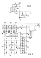
- the function of the circuit arrangement according to the invention is based on the consideration that it is shown in FIG. 1 It is fundamentally irrelevant on which side of a consumer 11 in the circuit a level influence is carried out if this level influence is intended to represent information transmission to the consumer 11. If an interruption of the circuit from the power source 12 via the load 11 is provided in particular for influencing the level, then either a current sink-side switch 13x or a current source-side switch 13y can be opened (briefly); because in both cases, the interruption of the circuit leads to the disappearance of the voltage drop across the load 11 in this circuit.
- the function modules 15 are connected via the intersections of matrix lines Xi and Yj. These function modules 15 are activated by two signals which are staggered in time, that is to say at a distance from one another, and which are sent to the crossing point on separate X-Y lines.
- the loads 11 are divided into a plurality of parallel circuits each equipped with at least one switch 13.
- the consumer side begins Evaluation of the decoding period by pressing (briefly opening) switch 13y; thereupon the switch 13xa for actuating the consumer 11a and after the corresponding (same or different) period b the switch 13xb for actuating the consumer 11b is actuated after the period a.
- consumers 11 can also be controlled individually if they are individualized by the same time periods for influencing the level; while, on the other hand, a quasi-parallel selection of consumers 11 is possible in this way, although these are individualized by different time periods of the level influencing.
- a particular consumer 11 ij is now to be addressed by a selection device 14, it only needs to be known in which coordinate ij this consumer 11 is connected to the bus system XY and by which level influence period this consumer 11 ij is individualized. Then, for example, the assigned switch 13xi and the other assigned switch 13yj is actuated by the individualization time offset. This results in a very high level of control security; because only one consumer 11 ij switched on in this coordinate crossing point between the bus lines Xi and Yj can be addressed, and this is actually only addressed if its specified individualization period corresponds to the actual time interval of the switch actuation 13xi-13yj.
- a plurality of consumers 11 i connected to the line Xi can be controlled in a targeted manner if the switches 13y located in the associated lines Y are actuated with a corresponding delay.
- the consumers 11 contain circuits with function modules 15, as will be explained in more detail below, cf. 3, these function modules 15 expediently receive their supply voltage via the connections of the XY lines from the power source 12.
- the modules 15 are preceded by a stabilization circuit 16 with a bypass memory 17, as is known as such from the circuit technology of regulated power supply units.
- the stabilization circuit 16 thus also delivers the functionally required operating voltage 18 for the uninterrupted operation of the function module 15 if (due to actuation of a switch 13, FIG. 2) the supply circuit in one of the lines X or Y is temporarily interrupted.
- a base load resistor 20 is switched on in the consumer 11 according to FIG. 3, parallel to the stabilization circuit 16, in the circuit of the lines X, Y via a decoupling diode 19. The voltage drop occurring over this is queried by the function module 15 via control lines 21.
- the consumer 11 supplies on a confirmation line 23 a decoding acknowledgment signal 24, which is delayed compared to the equipotential bonding on the lines 21 and in the example of FIG. 3 is used for the temporary activation of a burden 25 parallel to the base load resistor 20 in the circuit of the lines X-Y.
- This additional load then leads (FIG. 2) to a corresponding reduction in potential at a query circuit 26 when switches 13 are closed again, that is to say when the circuit is closed again via lines X-Y.
- This reduction in potential can be detected in a voltage detector 27 and implemented for outputting a drive acknowledgment signal 28 to the selection device 14.
- the burden 25 can simply be designed as an electronically controllable short-circuit switch 29 (shown in FIG. 3 as a field effect transistor).
- the query circuit 26 can basically consist of a decoupling resistor, in particular in the event of a short circuit to avoid overloading the power source 12, the use of a current limiting circuit 30 is more expedient there, as is basically known, for example, from the circuitry for overload protection of power supply units.
- a current limiting circuit 30 is more expedient there, as is basically known, for example, from the circuitry for overload protection of power supply units.
- each query circuit 26 is then connected to the voltage detector 27 or the selection device 14 via a query line 31, in addition to a query line 31.
- each consumer 11 and thus each functional module 15 is individualized by a defined period of time between two successive level changes caused by briefly opening switches 13.
- control signals are each caused by equipotential bonding between the control lines 21x-21y, that is to say in each case by one actuation (opening) of one of the switches 13.
- switch 13 by multiple actuation, to specify defined pulse series telegrams Ai or Bj (FIG. 2), which are in a decoding circuit must be verified in order to be able to start and control the time period tij.
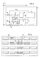
- FIG. 4 shows a typical application of an arrangement according to the invention, such as can occur in control rooms or with opto-electronic advertising media. It is, for example, a mosaic-like arrangement of intelligent displays 33 with actuating buttons 34 or 35 of input modules arranged in between, for example for manually influencing the displays on certain displays 33, which can be released individually by means of the central selection device 14 (FIG. 3).
- the proposed circuit arrangement for the targeted activation of function modules 15 and 15ij creates a matrix addressing method in which signals that are transmitted at different times and are transmitted on separate XY lines are connected via intersections of matrix lines Xi, Yi.
- Yi signaling switches 13xi, 13yi are used, to which in turn the supply lines X, Y are connected to the central power source 12.
- the function modules 15 and 15ij allow via the connected lines and those controlled accordingly Switches 13xi, 13yi that a transmission of data or signals or commands from a preferred computer or selection device 14 to them as well as from them to a computer or a selection device 14 is possible.
- This matrix addressing method thus creates the targeted activation of function modules 15 or 15ij as well as the targeted retrieval of specific function modules 15 or 15ij to a connected computer for the further processing of the data and commands received.
Landscapes
- Engineering & Computer Science (AREA)
- Computer Networks & Wireless Communication (AREA)
- Electronic Switches (AREA)
- Remote Monitoring And Control Of Power-Distribution Networks (AREA)
- Control By Computers (AREA)
Applications Claiming Priority (2)
| Application Number | Priority Date | Filing Date | Title |
|---|---|---|---|
| DE19863613108 DE3613108A1 (de) | 1986-04-18 | 1986-04-18 | Schaltungsanordnung zum gezielten ansteuern von funktionsmodulen ueber ein bus-system |
| DE3613108 | 1986-04-18 |
Publications (2)
| Publication Number | Publication Date |
|---|---|
| EP0242742A2 true EP0242742A2 (fr) | 1987-10-28 |
| EP0242742A3 EP0242742A3 (fr) | 1989-08-30 |
Family
ID=6298982
Family Applications (1)
| Application Number | Title | Priority Date | Filing Date |
|---|---|---|---|
| EP87105359A Withdrawn EP0242742A3 (fr) | 1986-04-18 | 1987-04-10 | Circuit pour la commande sélective de modules fonctionnels par un système bus |
Country Status (2)
| Country | Link |
|---|---|
| EP (1) | EP0242742A3 (fr) |
| DE (1) | DE3613108A1 (fr) |
Cited By (1)
| Publication number | Priority date | Publication date | Assignee | Title |
|---|---|---|---|---|
| US5796376A (en) * | 1991-12-18 | 1998-08-18 | Cie Research, Inc. | Electronic display sign |
Families Citing this family (2)
| Publication number | Priority date | Publication date | Assignee | Title |
|---|---|---|---|---|
| GB2243473B (en) * | 1990-04-27 | 1994-02-09 | Protech Instr And Systems Ltd | Data transmission and collection using a matrixed wire medium |
| WO1994013373A1 (fr) * | 1992-12-10 | 1994-06-23 | 'ecostroy' Co. Ltd. | Ecran d'affichage en couleur dynamique |
Family Cites Families (3)
| Publication number | Priority date | Publication date | Assignee | Title |
|---|---|---|---|---|
| GB1589748A (en) * | 1976-09-10 | 1981-05-20 | Matsushita Electric Works Ltd | Time division multiplex transmission system |
| DE2812896C2 (de) * | 1977-03-28 | 1983-10-27 | Ricoh Co., Ltd., Tokyo | Datenerfassungseinrichtung |
| DE3012045C2 (de) * | 1980-03-28 | 1985-01-31 | Nsm-Apparatebau Gmbh & Co Kg, 6530 Bingen | Anordnung und Verfahren zum Ein- und Ausschalten einer Vielzahl von an einer Spannungsquelle angeschlossenen Verbrauchern |
-
1986
- 1986-04-18 DE DE19863613108 patent/DE3613108A1/de active Granted
-
1987
- 1987-04-10 EP EP87105359A patent/EP0242742A3/fr not_active Withdrawn
Cited By (1)
| Publication number | Priority date | Publication date | Assignee | Title |
|---|---|---|---|---|
| US5796376A (en) * | 1991-12-18 | 1998-08-18 | Cie Research, Inc. | Electronic display sign |
Also Published As
| Publication number | Publication date |
|---|---|
| DE3613108C2 (fr) | 1988-11-10 |
| EP0242742A3 (fr) | 1989-08-30 |
| DE3613108A1 (de) | 1987-10-22 |
Similar Documents
| Publication | Publication Date | Title |
|---|---|---|
| EP0535205A1 (fr) | Installation de surveillance pour un dispositif de commande. | |
| DE3623705C2 (fr) | ||
| CH675036A5 (fr) | ||
| EP0242742A2 (fr) | Circuit pour la commande sélective de modules fonctionnels par un système bus | |
| EP0532787B1 (fr) | Dispositif pour l'opération de détecteurs de dangers | |
| EP2494534B1 (fr) | Système de communication de sécurité pour signaler des états du système | |
| DE19631302B4 (de) | Sensor-Aktor-Bussystem | |
| DE19955632A1 (de) | Sicherheitsschaltung | |
| DE3315683C1 (de) | Schaltungsanordnung zum Abfragen einer Matrix aus Tastenkontakten | |
| DE2652919C2 (de) | Vorrichtung zur folgegebundenen Auslösung mehrerer stabiler Zustände, insbesondere der Beleuchtungseinrichtung eines Kraftfahrzeuges | |
| DE2718473C3 (de) | Schaltungsanordnung zum parallelen Übertragen von Signalen über mehrere parallele Leitungen | |
| EP0202684B1 (fr) | Procédé pour la commande sélective de circuits électriques ainsi que montage pour l'exécution du procédé | |
| DE2207707A1 (de) | Schaltungszelle fur Steuerschaltungen | |
| CH646535A5 (en) | Circuit arrangement for controlling a relay with signal protection | |
| EP0450119A1 (fr) | Dispositif pour raccorder des éléments additionnels à une ligne servant à la surveillance et déjà existante | |
| DE3441371A1 (de) | Zentrale steuerelektronikschaltung fuer rolladenmotoren | |
| DE2536946A1 (de) | Ueberwachungssystem zur ueberwachung von ferneinheiten | |
| EP0191421B1 (fr) | Circuit de surveillance pour signaux numériques | |
| EP2515553B1 (fr) | Système de communication de sécurité destiné à la signalisation d'états du système | |
| EP0195457A1 (fr) | Dispositif et autosurveillance d'un circuit à microprocesseur | |
| DE4303048A1 (en) | Alarm recognition apparatus for redundant layout circuit in radio equipment - has input circuits delaying alarm recognition signals when circuits are switched to be operational systems | |
| EP1157468B1 (fr) | Systeme et procede pour determiner si la valeur de comptage d'un compteur a atteint ou non une valeur de comptage predefinie | |
| DE2449634A1 (de) | Informations-erfassungssystem | |
| EP1101154B1 (fr) | Unite de commande electrique | |
| DE2823919C3 (de) | Anordnung zur Abfrage mehrerer Gruppen von Meldequellen mittels einer Signalisierungseinheit |
Legal Events
| Date | Code | Title | Description |
|---|---|---|---|
| PUAI | Public reference made under article 153(3) epc to a published international application that has entered the european phase |
Free format text: ORIGINAL CODE: 0009012 |
|
| AK | Designated contracting states |
Kind code of ref document: A2 Designated state(s): AT BE CH DE ES FR GB GR IT LI LU NL SE |
|
| PUAL | Search report despatched |
Free format text: ORIGINAL CODE: 0009013 |
|
| AK | Designated contracting states |
Kind code of ref document: A3 Designated state(s): AT BE CH DE ES FR GB GR IT LI LU NL SE |
|
| 17P | Request for examination filed |
Effective date: 19890822 |
|
| 17Q | First examination report despatched |
Effective date: 19920113 |
|
| STAA | Information on the status of an ep patent application or granted ep patent |
Free format text: STATUS: THE APPLICATION IS DEEMED TO BE WITHDRAWN |
|
| 18D | Application deemed to be withdrawn |
Effective date: 19920526 |
|
| RIN1 | Information on inventor provided before grant (corrected) |
Inventor name: KEMPER, ROLF |