EP0243057A1 - Module de transmission optique - Google Patents
Module de transmission optique Download PDFInfo
- Publication number
- EP0243057A1 EP0243057A1 EP87303190A EP87303190A EP0243057A1 EP 0243057 A1 EP0243057 A1 EP 0243057A1 EP 87303190 A EP87303190 A EP 87303190A EP 87303190 A EP87303190 A EP 87303190A EP 0243057 A1 EP0243057 A1 EP 0243057A1
- Authority
- EP
- European Patent Office
- Prior art keywords
- mount
- sub
- fibre
- package
- optical
- Prior art date
- Legal status (The legal status is an assumption and is not a legal conclusion. Google has not performed a legal analysis and makes no representation as to the accuracy of the status listed.)
- Ceased
Links
- 230000003287 optical effect Effects 0.000 title claims description 16
- 230000005540 biological transmission Effects 0.000 title claims description 14
- 239000000835 fiber Substances 0.000 claims abstract description 27
- 239000013307 optical fiber Substances 0.000 claims abstract description 16
- 229910000679 solder Inorganic materials 0.000 claims abstract description 15
- 238000010438 heat treatment Methods 0.000 claims abstract description 7
- 238000010276 construction Methods 0.000 claims description 7
- 239000004065 semiconductor Substances 0.000 claims description 6
- 239000000853 adhesive Substances 0.000 claims description 4
- 230000001070 adhesive effect Effects 0.000 claims description 4
- 238000000034 method Methods 0.000 claims description 2
- 239000000758 substrate Substances 0.000 claims description 2
- 238000012216 screening Methods 0.000 claims 1
- 238000002347 injection Methods 0.000 abstract description 17
- 239000007924 injection Substances 0.000 abstract description 17
- 239000004020 conductor Substances 0.000 abstract description 13
- 230000006355 external stress Effects 0.000 abstract 1
- PCHJSUWPFVWCPO-UHFFFAOYSA-N gold Chemical compound [Au] PCHJSUWPFVWCPO-UHFFFAOYSA-N 0.000 description 5
- 239000010931 gold Substances 0.000 description 5
- 229910052737 gold Inorganic materials 0.000 description 5
- 239000000976 ink Substances 0.000 description 5
- 238000004519 manufacturing process Methods 0.000 description 5
- 238000000429 assembly Methods 0.000 description 4
- 238000012544 monitoring process Methods 0.000 description 3
- 239000000919 ceramic Substances 0.000 description 2
- 229910052751 metal Inorganic materials 0.000 description 2
- 239000002184 metal Substances 0.000 description 2
- 230000002411 adverse Effects 0.000 description 1
- PNEYBMLMFCGWSK-UHFFFAOYSA-N aluminium oxide Inorganic materials [O-2].[O-2].[O-2].[Al+3].[Al+3] PNEYBMLMFCGWSK-UHFFFAOYSA-N 0.000 description 1
- 230000004888 barrier function Effects 0.000 description 1
- 150000001875 compounds Chemical class 0.000 description 1
- 238000001816 cooling Methods 0.000 description 1
- 230000008878 coupling Effects 0.000 description 1
- 238000010168 coupling process Methods 0.000 description 1
- 238000005859 coupling reaction Methods 0.000 description 1
- 239000003822 epoxy resin Substances 0.000 description 1
- 239000011521 glass Substances 0.000 description 1
- JUWSSMXCCAMYGX-UHFFFAOYSA-N gold platinum Chemical compound [Pt].[Au] JUWSSMXCCAMYGX-UHFFFAOYSA-N 0.000 description 1
- NJPPVKZQTLUDBO-UHFFFAOYSA-N novaluron Chemical compound C1=C(Cl)C(OC(F)(F)C(OC(F)(F)F)F)=CC=C1NC(=O)NC(=O)C1=C(F)C=CC=C1F NJPPVKZQTLUDBO-UHFFFAOYSA-N 0.000 description 1
- 239000004033 plastic Substances 0.000 description 1
- 229920003023 plastic Polymers 0.000 description 1
- 229920000647 polyepoxide Polymers 0.000 description 1
- 150000003304 ruthenium compounds Chemical class 0.000 description 1
- 238000000926 separation method Methods 0.000 description 1
- 230000035882 stress Effects 0.000 description 1
- 230000008646 thermal stress Effects 0.000 description 1
- 230000000007 visual effect Effects 0.000 description 1
Images


Classifications
-
- G—PHYSICS
- G02—OPTICS
- G02B—OPTICAL ELEMENTS, SYSTEMS OR APPARATUS
- G02B6/00—Light guides; Structural details of arrangements comprising light guides and other optical elements, e.g. couplings
- G02B6/24—Coupling light guides
- G02B6/42—Coupling light guides with opto-electronic elements
- G02B6/4201—Packages, e.g. shape, construction, internal or external details
- G02B6/4248—Feed-through connections for the hermetical passage of fibres through a package wall
-
- G—PHYSICS
- G02—OPTICS
- G02B—OPTICAL ELEMENTS, SYSTEMS OR APPARATUS
- G02B6/00—Light guides; Structural details of arrangements comprising light guides and other optical elements, e.g. couplings
- G02B6/24—Coupling light guides
- G02B6/42—Coupling light guides with opto-electronic elements
- G02B6/4201—Packages, e.g. shape, construction, internal or external details
- G02B6/4202—Packages, e.g. shape, construction, internal or external details for coupling an active element with fibres without intermediate optical elements, e.g. fibres with plane ends, fibres with shaped ends, bundles
-
- G—PHYSICS
- G02—OPTICS
- G02B—OPTICAL ELEMENTS, SYSTEMS OR APPARATUS
- G02B6/00—Light guides; Structural details of arrangements comprising light guides and other optical elements, e.g. couplings
- G02B6/24—Coupling light guides
- G02B6/42—Coupling light guides with opto-electronic elements
- G02B6/4201—Packages, e.g. shape, construction, internal or external details
- G02B6/4219—Mechanical fixtures for holding or positioning the elements relative to each other in the couplings; Alignment methods for the elements, e.g. measuring or observing methods especially used therefor
- G02B6/4236—Fixing or mounting methods of the aligned elements
- G02B6/4238—Soldering
-
- G—PHYSICS
- G02—OPTICS
- G02B—OPTICAL ELEMENTS, SYSTEMS OR APPARATUS
- G02B6/00—Light guides; Structural details of arrangements comprising light guides and other optical elements, e.g. couplings
- G02B6/24—Coupling light guides
- G02B6/42—Coupling light guides with opto-electronic elements
- G02B6/4201—Packages, e.g. shape, construction, internal or external details
- G02B6/4219—Mechanical fixtures for holding or positioning the elements relative to each other in the couplings; Alignment methods for the elements, e.g. measuring or observing methods especially used therefor
- G02B6/422—Active alignment, i.e. moving the elements in response to the detected degree of coupling or position of the elements
- G02B6/4221—Active alignment, i.e. moving the elements in response to the detected degree of coupling or position of the elements involving a visual detection of the position of the elements, e.g. by using a microscope or a camera
- G02B6/4224—Active alignment, i.e. moving the elements in response to the detected degree of coupling or position of the elements involving a visual detection of the position of the elements, e.g. by using a microscope or a camera using visual alignment markings, e.g. index methods
Definitions
- This invention relates to the manufacture of an optical transmission package, and in particular although not exclusively to the manufacture of hermetically sealed injection laser packages with single mode optical fibre tails, especially, but not exclusively, for use in telecommunications systems and data links.
- the fibre support tube which carries the optical fibre up to a point very close to the laser can be subjected to stress through temperature changes of the package and external forces on the package.
- a discrete thermistor can be employed within the package to monitor the temperature, and a heat pump mounted between the sub-assemblies supporting the tube and the laser package can attempt to maintain the sub-assemblies within a pre-set temperature range to minimise the thermal stress, nevertheless the hermetic tube tends to transmit heat along it from the outer package casing directing to the sub-assembly and very close to the interface between the fibre end and the laser, causing local heating or local cooling if the hermetic outer casing of the package suffers extremes of temperature. That is to say that the thermistor mounted on one of the sub-assemblies may not in fact be sensing the actual local temperature in the vincinity of these critical regions.
- an optical transmission package comprising a housing having an entrance for an optical fibre, a sub-mount within the housing, an optical fibre extending through the entrance and onto the sub-mount, and a semiconductor optical transmission device in direct light-transfer-connection with the end of the fibre, the sub-mount comprising a plurality of films formed one on top of the other and the fibre being secured to the sub-mount by an adhesive.
- a multi-layer thick film construction one of said layers within said construction being a resistive layer which can be used as a heating element, there being connection terminals connected with said element whereby an electric current can be passed through the element to heat the mounting arrangement.
- a large ceramic piece (e.g. 5cm x 5cm or 10cm x10cm) which will form several substrates such as l is screen printed with thick film gold pads to form ground planes on the back and then the front is screen printed with several thick film gold "patterns" and as shown in Fig. 1 and each comprising a connection pattern of conductors and a ground plane 2.
- This is done using standard thick film gold printing at 8-12um fired thickness. This printing also "plates through” two via holes to connect to ground planes 2 with the bottom ground planes.
- the channels between the several patterns are used for laser scribing. After the final prints and separation the two longer edges are printed with gold ink to further connect the upper ground plane 2 with the lower ground plane. This is for better operation at very high bit rate working.
- One portion 2A of the ground plane 2 forms the base for a sub-mount formed solely of thick film inks and dielectric which are fired to provide a platform at the correct level on which is mounted the end portion of the fibre tail.
- the first layer of this sub-mount which with reference to Fig. 2 can be more clearly understood, comprises a dielectric layer 3 to provide an electrically insulating layer.
- the dielectric comprises for example glass and alumina and is fired at a temperature of approximately 850°C.
- the dielectric 3 forms an insulating layer for insulating the conductors 4A and 4B from each other and from the ground plane.
- resistive thick film ink for example a ruthenium compound
- a second dielectric layer 6 On top of the resistive layer 5 and the outer edge regions of the conductors 4A and 4B is a second dielectric layer 6, similar to the layer 3.
- solder pad 7 of a platinum gold ink compound.
- the width of this pad is small and only a few times wider than the diameter of the fibre which is to be soldered.
- the fibre diameter is 130 ⁇ m and the width of the track is approximately 500 ⁇ m.
- thermistor element 8 In addition to the sub-mount for the fibre there is also screen-printed a pair of thermistor elements 8 and 9, thermistor element 8 being printed onto top and bottom printed conductor 10 and 11 with an overglaze 12 and similarly thermistor element 9 is printed at its upper end as viewed in Fig. 1 onto a portion of ground plane 2 and at its lower end onto etched conductor 13. An overglaze 14 is provided to protect the thermistor element.
- one or other of the thermistor element is connected via external circuitry to control a heat pump in the package for maintaining the mount, particularly the laser chip, within a close band of temperatures. Where temperature control is not necessary, then the heat pump will be omitted and the thermistor elements will not be connected in circuit.
- the visual location markers 15 indicate approximately the position to be occupied by the injection laser header on which is mounted the injection laser chip.
- the visible location markers 16 indicate the approximate location of a monitor block containing a monitoring photodiode which will receive the back-light from the injection laser and, via external control circuitry, is used to monitor the laser performance and control the bias current applied to the laser so that, when the output power of the laser falls with age, the bias current can be changed to increase the laser output and thereby maintain a substantially constant output throughout the working life of the laser.
- the monitor block is indicated by the reference numeral 17.
- the printed conductor patterns 18, 19 and 20 are connected via wire bonding to the laser chip and the monitor block for onward connection to the upper ends of the DIL external connection terminals 31 shown more clearly in Fig. 3.
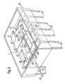
- FIG. 3 (which is not drawn to scale) there is shown an injection laser package with the lid removed for clarity.
- the package comprises a box-like housing 30 having 14 connection terminals such as 31 extending through the base (not shown) to the interior of the housing 30.
- the ceramic mount indicated in Fig. 3 generally by reference numeral 1, is supported inside the housing 30 on a heat pump 32 which is secured on the base of the box, on the one hand, and to the underside of the mount 1 on the other hand.
- the heat pump 32 would be replaced by a simple metal block where close temperature control of the electro-optical transducer i.e. laser ELED or other optical transmitting/receiving device, is not necessary.
- the monitor 17 is located as shown to monitor the rear output of the laser 33 mounted on its header 34 on the mount 1. In some applications the monitor 17 would not be required.
- an extrance support tube 35 welded to the housing 30 and providing a rigid support for an optical fibre tail 36 which optically connects the electro-optic transducer with the outside world.
- An end portion 36A lies on the solder pad 7 and the portion of the fibre which extends through the tube 35 is secured in the tube, for example by solder or epoxy resin adhesive.
- the optical fibre end portion 36A is aligned with the laser chip 33, in the particular embodiment described an injection laser.
- an electrical source is applied to the conductors 4A and 4B which heats up the resistor layer 5 in the optical fibre sub-mount. This heating is sufficient to melt the solder pad and thereby solder the fibre to its sub-mount directly in alignment with the injection laser.
- the height of the top of the solder pad will be fixed by manufacture and will have a tolerance.
- the height of the emitting area of the laser above the sub-mount will be fixed by the pedestal, solder fillet thickness etc and will have a tolerance.
- In assembling the package we support the fibre in space above the solder pad either by a vacuum and/or mechanical grippers to locate the optimum position. When the solder infill freezes it pulls the fibre down so prior to solder infill we:-
- the film circuit techniques adopted for the mount 1 provide a significant simplification to the construction of an injection laser package and at the same time provide precise geometric control particularly for the alignment of the fibre with the injection laser chip.
- the transmission package could function either as a transmitter or a receiver.
- the multi-layer thick film mounting arrangement described has other applications beyond that of the transmission package described.
- the buried resistive layer could be used for local temperature control in e.g. test equipment or circuits or parts of circuits for use in sub-zero environments.
Landscapes
- Physics & Mathematics (AREA)
- General Physics & Mathematics (AREA)
- Optics & Photonics (AREA)
- Optical Couplings Of Light Guides (AREA)
- Semiconductor Lasers (AREA)
- Led Device Packages (AREA)
- Light Guides In General And Applications Therefor (AREA)
- Led Devices (AREA)
Applications Claiming Priority (2)
| Application Number | Priority Date | Filing Date | Title |
|---|---|---|---|
| GB8609858 | 1986-04-23 | ||
| GB8609858A GB2189620B (en) | 1986-04-23 | 1986-04-23 | Optical fibre transmission package |
Publications (1)
| Publication Number | Publication Date |
|---|---|
| EP0243057A1 true EP0243057A1 (fr) | 1987-10-28 |
Family
ID=10596662
Family Applications (1)
| Application Number | Title | Priority Date | Filing Date |
|---|---|---|---|
| EP87303190A Ceased EP0243057A1 (fr) | 1986-04-23 | 1987-04-13 | Module de transmission optique |
Country Status (4)
| Country | Link |
|---|---|
| US (1) | US4844581A (fr) |
| EP (1) | EP0243057A1 (fr) |
| JP (1) | JPS6319610A (fr) |
| GB (1) | GB2189620B (fr) |
Cited By (5)
| Publication number | Priority date | Publication date | Assignee | Title |
|---|---|---|---|---|
| EP0356988A3 (fr) * | 1988-08-31 | 1991-03-20 | Sumitomo Electric Industries, Ltd. | Un dispositif pour la fabrication d'un module de transmission optique |
| EP0579439A1 (fr) * | 1992-07-16 | 1994-01-19 | AT&T Corp. | Article comprenant un laser couplé avec une fibre optique |
| EP0704730A1 (fr) * | 1994-09-29 | 1996-04-03 | CSELT Centro Studi e Laboratori Telecomunicazioni S.p.A. | Module de transmission pour interconnexion optique |
| US5596664A (en) * | 1994-09-29 | 1997-01-21 | Cselt-Centro E Laboratori Telecomunicazioni S.P.A. | Transmitter module for optical interconnections |
| EP1365488A3 (fr) * | 1998-02-27 | 2004-02-18 | Litton Systems, Inc. | Méthode d'empaquetage d'une assemblage de sous-support |
Families Citing this family (40)
| Publication number | Priority date | Publication date | Assignee | Title |
|---|---|---|---|---|
| US4997253A (en) * | 1989-04-03 | 1991-03-05 | Tektronix, Inc. | Electro-optical transducer module and a method of fabricating such a module |
| US5073000A (en) * | 1990-05-21 | 1991-12-17 | Motorola, Inc. | Optical interconnect printed circuit structure |
| US5182782A (en) * | 1990-07-11 | 1993-01-26 | Gte Laboratories Incorporated | Waferboard structure and method of fabricating |
| US5268066A (en) * | 1990-07-11 | 1993-12-07 | Gte Laboratories Incorporated | Method of fabricating waferboard structure |
| US5163108A (en) * | 1990-07-11 | 1992-11-10 | Gte Laboratories Incorporated | Method and device for passive alignment of diode lasers and optical fibers |
| US5155786A (en) * | 1991-04-29 | 1992-10-13 | International Business Machines Corporation | Apparatus and a method for an optical fiber interface |
| US5241614A (en) * | 1991-04-29 | 1993-08-31 | International Business Machines Corporation | Apparatus and a method for an optical fiber interface |
| US5434940A (en) * | 1994-03-24 | 1995-07-18 | The Whitaker Corporation | Active fiber needle |
| USRE40150E1 (en) | 1994-04-25 | 2008-03-11 | Matsushita Electric Industrial Co., Ltd. | Fiber optic module |
| US6220878B1 (en) | 1995-10-04 | 2001-04-24 | Methode Electronics, Inc. | Optoelectronic module with grounding means |
| US5546281A (en) | 1995-01-13 | 1996-08-13 | Methode Electronics, Inc. | Removable optoelectronic transceiver module with potting box |
| US5717533A (en) | 1995-01-13 | 1998-02-10 | Methode Electronics Inc. | Removable optoelectronic module |
| US6203333B1 (en) | 1998-04-22 | 2001-03-20 | Stratos Lightwave, Inc. | High speed interface converter module |
| US6179627B1 (en) | 1998-04-22 | 2001-01-30 | Stratos Lightwave, Inc. | High speed interface converter module |
| US6164837A (en) * | 1998-12-30 | 2000-12-26 | Mcdonnell Douglas Corporation | Integrated microelectromechanical alignment and locking apparatus and method for fiber optic module manufacturing |
| US6873800B1 (en) | 1999-05-26 | 2005-03-29 | Jds Uniphase Corporation | Hot pluggable optical transceiver in a small form pluggable package |
| US6901221B1 (en) | 1999-05-27 | 2005-05-31 | Jds Uniphase Corporation | Method and apparatus for improved optical elements for vertical PCB fiber optic modules |
| US6213651B1 (en) | 1999-05-26 | 2001-04-10 | E20 Communications, Inc. | Method and apparatus for vertical board construction of fiber optic transmitters, receivers and transceivers |
| US7013088B1 (en) | 1999-05-26 | 2006-03-14 | Jds Uniphase Corporation | Method and apparatus for parallel optical interconnection of fiber optic transmitters, receivers and transceivers |
| US6632030B2 (en) | 1999-05-27 | 2003-10-14 | E20 Communications, Inc. | Light bending optical block for fiber optic modules |
| US20020030872A1 (en) * | 1999-05-27 | 2002-03-14 | Edwin Dair | Method and apparatus for multiboard fiber optic modules and fiber optic module arrays |
| US7116912B2 (en) * | 1999-05-27 | 2006-10-03 | Jds Uniphase Corporation | Method and apparatus for pluggable fiber optic modules |
| US20020033979A1 (en) * | 1999-05-27 | 2002-03-21 | Edwin Dair | Method and apparatus for multiboard fiber optic modules and fiber optic module arrays |
| US20010048793A1 (en) * | 1999-05-27 | 2001-12-06 | Edwin Dair | Method and apparatus for multiboard fiber optic modules and fiber optic module arrays |
| US20040069997A1 (en) * | 1999-05-27 | 2004-04-15 | Edwin Dair | Method and apparatus for multiboard fiber optic modules and fiber optic module arrays |
| US20010030789A1 (en) * | 1999-05-27 | 2001-10-18 | Wenbin Jiang | Method and apparatus for fiber optic modules |
| US6952532B2 (en) * | 1999-05-27 | 2005-10-04 | Jds Uniphase Corporation | Method and apparatus for multiboard fiber optic modules and fiber optic module arrays |
| US7090509B1 (en) | 1999-06-11 | 2006-08-15 | Stratos International, Inc. | Multi-port pluggable transceiver (MPPT) with multiple LC duplex optical receptacles |
| US6220873B1 (en) | 1999-08-10 | 2001-04-24 | Stratos Lightwave, Inc. | Modified contact traces for interface converter |
| US6325551B1 (en) | 1999-12-08 | 2001-12-04 | New Focus, Inc. | Method and apparatus for optically aligning optical fibers with optical devices |
| US6632029B1 (en) | 1999-12-22 | 2003-10-14 | New Focus, Inc. | Method & apparatus for packaging high frequency components |
| JP2002094168A (ja) * | 2000-09-19 | 2002-03-29 | Toshiba Corp | 半導体レーザ装置及びその製造方法 |
| US6423939B1 (en) * | 2000-10-02 | 2002-07-23 | Agilent Technologies, Inc. | Micro soldering method and apparatus |
| US6549548B2 (en) * | 2000-10-25 | 2003-04-15 | Axsun Technologies, Inc. | Interferometric filter wavelength meter and controller |
| US6459710B1 (en) | 2000-11-07 | 2002-10-01 | Axsun Technologies, Inc. | Reflector for directing front facet light to monitor diode |
| US6846113B2 (en) * | 2002-05-17 | 2005-01-25 | Archcom Technology, Inc. | Packaging for high power pump laser modules |
| US20040114882A1 (en) * | 2002-12-12 | 2004-06-17 | Marquez Christian L. | Low cost integrated heater substrate for active optical fiber alignment |
| EP1942358A2 (fr) * | 2006-12-27 | 2008-07-09 | JDS Uniphase Corporation | Ensemble de composants et procédé de fabrication |
| FR2912029B1 (fr) * | 2007-01-31 | 2010-10-22 | Hispano Suiza Sa | Carte electronique incorporant une resistance chauffante. |
| CN102909452B (zh) * | 2012-11-12 | 2014-09-17 | 镇江市松协电器有限公司 | 一种导电片与导线的焊接装置 |
Citations (3)
| Publication number | Priority date | Publication date | Assignee | Title |
|---|---|---|---|---|
| CA1151277A (fr) * | 1981-02-11 | 1983-08-02 | Northern Telecom Limited | Methode de fixation d'une fibre optique dans un boitier de laser hermetique |
| FR2582413A1 (fr) * | 1985-05-23 | 1986-11-28 | Comp Generale Electricite | Procede de couplage d'une fibre optique a un composant optoelectronique sur une embase |
| FR2584827A1 (fr) * | 1985-07-09 | 1987-01-16 | Comp Generale Electricite | Dispositif de couplage d'une fibre optique a un composant optoelectronique |
Family Cites Families (8)
| Publication number | Priority date | Publication date | Assignee | Title |
|---|---|---|---|---|
| US4130343A (en) * | 1977-02-22 | 1978-12-19 | Bell Telephone Laboratories, Incorporated | Coupling arrangements between a light-emitting diode and an optical fiber waveguide and between an optical fiber waveguide and a semiconductor optical detector |
| US4296998A (en) * | 1979-12-17 | 1981-10-27 | Bell Telephone Laboratories, Incorporated | Encapsulated light source with coupled fiberguide |
| GB2124402B (en) * | 1982-07-27 | 1986-01-22 | Standard Telephones Cables Ltd | Injection laser packages |
| GB2131971B (en) * | 1982-12-14 | 1986-12-10 | Plessey Co Plc | Positioning an optical fibre relative to an opto-electronic device |
| US4585304A (en) * | 1983-09-06 | 1986-04-29 | Virginia | Technique for repairing and joining small diameter optical fiber cables |
| JPS61189657A (ja) * | 1985-02-18 | 1986-08-23 | Fuji Photo Film Co Ltd | 半導体素子温度制御装置 |
| US4722586A (en) * | 1985-04-12 | 1988-02-02 | Tektronix, Inc. | Electro-optical transducer module |
| WO1987002833A1 (fr) * | 1985-10-28 | 1987-05-07 | American Telephone & Telegraph Company | Module de laser ceramique multi-couches |
-
1986
- 1986-04-23 GB GB8609858A patent/GB2189620B/en not_active Expired - Fee Related
-
1987
- 1987-04-13 EP EP87303190A patent/EP0243057A1/fr not_active Ceased
- 1987-04-21 JP JP62098496A patent/JPS6319610A/ja active Pending
- 1987-04-22 US US07/041,218 patent/US4844581A/en not_active Expired - Fee Related
Patent Citations (3)
| Publication number | Priority date | Publication date | Assignee | Title |
|---|---|---|---|---|
| CA1151277A (fr) * | 1981-02-11 | 1983-08-02 | Northern Telecom Limited | Methode de fixation d'une fibre optique dans un boitier de laser hermetique |
| FR2582413A1 (fr) * | 1985-05-23 | 1986-11-28 | Comp Generale Electricite | Procede de couplage d'une fibre optique a un composant optoelectronique sur une embase |
| FR2584827A1 (fr) * | 1985-07-09 | 1987-01-16 | Comp Generale Electricite | Dispositif de couplage d'une fibre optique a un composant optoelectronique |
Cited By (5)
| Publication number | Priority date | Publication date | Assignee | Title |
|---|---|---|---|---|
| EP0356988A3 (fr) * | 1988-08-31 | 1991-03-20 | Sumitomo Electric Industries, Ltd. | Un dispositif pour la fabrication d'un module de transmission optique |
| EP0579439A1 (fr) * | 1992-07-16 | 1994-01-19 | AT&T Corp. | Article comprenant un laser couplé avec une fibre optique |
| EP0704730A1 (fr) * | 1994-09-29 | 1996-04-03 | CSELT Centro Studi e Laboratori Telecomunicazioni S.p.A. | Module de transmission pour interconnexion optique |
| US5596664A (en) * | 1994-09-29 | 1997-01-21 | Cselt-Centro E Laboratori Telecomunicazioni S.P.A. | Transmitter module for optical interconnections |
| EP1365488A3 (fr) * | 1998-02-27 | 2004-02-18 | Litton Systems, Inc. | Méthode d'empaquetage d'une assemblage de sous-support |
Also Published As
| Publication number | Publication date |
|---|---|
| GB2189620A (en) | 1987-10-28 |
| US4844581A (en) | 1989-07-04 |
| GB2189620B (en) | 1990-03-28 |
| JPS6319610A (ja) | 1988-01-27 |
| GB8609858D0 (en) | 1986-05-29 |
Similar Documents
| Publication | Publication Date | Title |
|---|---|---|
| US4844581A (en) | Optical transmission package | |
| US7215886B2 (en) | Optical communication module | |
| US6932522B2 (en) | Method and apparatus for hermetically sealing photonic devices | |
| EP1022822B1 (fr) | Module optique | |
| US7275937B2 (en) | Optoelectronic module with components mounted on a flexible circuit | |
| US6467972B2 (en) | Optical interconnection module | |
| US6513993B1 (en) | Optical communications device | |
| US7306377B2 (en) | Integrated optical sub-assembly having epoxy chip package | |
| EP0726477A2 (fr) | Arrangement pour connecter une fibre optique avec un composant optique | |
| US7103249B2 (en) | Optical module and manufacturing method of the same, optical-communication apparatus, and electronic apparatus | |
| EP1701189A1 (fr) | Procédé de fabrication d'un module optique comprenant un composant de protection avec câblage électrique | |
| US7039083B2 (en) | High speed optical transmission assembly | |
| JP2002359426A (ja) | 光モジュール及び光通信システム | |
| JPH0714102B2 (ja) | 光結合装置 | |
| KR100426039B1 (ko) | 칩 실장방법 및 장치 | |
| US7366367B2 (en) | Optical data link and method of manufacturing optical data link | |
| US6796723B2 (en) | Submount for opto-electronic module and packaging method using the same | |
| US6827505B2 (en) | Optoelectronic package structure and process for planar passive optical and optoelectronic devices | |
| JP2004093606A (ja) | 光モジュール及び光伝送装置 | |
| CA1328183C (fr) | Module optique | |
| JPH1152193A (ja) | 光半導体モジュール | |
| US7226216B2 (en) | Optoelectronic transmission and/or reception arrangement | |
| CA2159041C (fr) | Module d'emission pour les interconnexions optiques | |
| JP4798863B2 (ja) | 光電気配線基板 | |
| EP0704730B1 (fr) | Module de transmission pour interconnexion optique |
Legal Events
| Date | Code | Title | Description |
|---|---|---|---|
| PUAI | Public reference made under article 153(3) epc to a published international application that has entered the european phase |
Free format text: ORIGINAL CODE: 0009012 |
|
| AK | Designated contracting states |
Kind code of ref document: A1 Designated state(s): AT BE DE FR IT NL |
|
| 17P | Request for examination filed |
Effective date: 19880321 |
|
| 17Q | First examination report despatched |
Effective date: 19891204 |
|
| STAA | Information on the status of an ep patent application or granted ep patent |
Free format text: STATUS: THE APPLICATION HAS BEEN REFUSED |
|
| 18R | Application refused |
Effective date: 19910913 |
|
| RIN1 | Information on inventor provided before grant (corrected) |
Inventor name: TURNER, ANDREW STEPHEN |