EP0243157A2 - Bildaufnahmegerät - Google Patents
Bildaufnahmegerät Download PDFInfo
- Publication number
- EP0243157A2 EP0243157A2 EP87303515A EP87303515A EP0243157A2 EP 0243157 A2 EP0243157 A2 EP 0243157A2 EP 87303515 A EP87303515 A EP 87303515A EP 87303515 A EP87303515 A EP 87303515A EP 0243157 A2 EP0243157 A2 EP 0243157A2
- Authority
- EP
- European Patent Office
- Prior art keywords
- image pickup
- signal
- pickup device
- read
- gain
- Prior art date
- Legal status (The legal status is an assumption and is not a legal conclusion. Google has not performed a legal analysis and makes no representation as to the accuracy of the status listed.)
- Granted
Links
- 238000012545 processing Methods 0.000 claims description 28
- 230000001066 destructive effect Effects 0.000 claims description 4
- 229940000425 combination drug Drugs 0.000 claims 1
- 238000000034 method Methods 0.000 description 10
- 238000010586 diagram Methods 0.000 description 8
- 230000003247 decreasing effect Effects 0.000 description 5
- 230000002238 attenuated effect Effects 0.000 description 3
- 238000012937 correction Methods 0.000 description 3
- 238000001514 detection method Methods 0.000 description 3
- 230000005855 radiation Effects 0.000 description 3
- 239000004065 semiconductor Substances 0.000 description 3
- 238000012546 transfer Methods 0.000 description 3
- 230000003321 amplification Effects 0.000 description 2
- 239000003990 capacitor Substances 0.000 description 2
- 230000001276 controlling effect Effects 0.000 description 2
- 230000010354 integration Effects 0.000 description 2
- 238000003199 nucleic acid amplification method Methods 0.000 description 2
- 238000005375 photometry Methods 0.000 description 2
- 239000000758 substrate Substances 0.000 description 2
- VYPSYNLAJGMNEJ-UHFFFAOYSA-N Silicium dioxide Chemical compound O=[Si]=O VYPSYNLAJGMNEJ-UHFFFAOYSA-N 0.000 description 1
- 238000009825 accumulation Methods 0.000 description 1
- 230000015572 biosynthetic process Effects 0.000 description 1
- 230000015556 catabolic process Effects 0.000 description 1
- 239000002131 composite material Substances 0.000 description 1
- 230000002950 deficient Effects 0.000 description 1
- 238000006731 degradation reaction Methods 0.000 description 1
- 230000000994 depressogenic effect Effects 0.000 description 1
- 238000011161 development Methods 0.000 description 1
- 230000018109 developmental process Effects 0.000 description 1
- 238000005286 illumination Methods 0.000 description 1
- 230000006698 induction Effects 0.000 description 1
- 210000003127 knee Anatomy 0.000 description 1
- 238000012856 packing Methods 0.000 description 1
- 230000003071 parasitic effect Effects 0.000 description 1
- 230000001105 regulatory effect Effects 0.000 description 1
- 229910052710 silicon Inorganic materials 0.000 description 1
- 239000010703 silicon Substances 0.000 description 1
- 229910052814 silicon oxide Inorganic materials 0.000 description 1
- 230000003068 static effect Effects 0.000 description 1
Images



Classifications
-
- H—ELECTRICITY
- H04—ELECTRIC COMMUNICATION TECHNIQUE
- H04N—PICTORIAL COMMUNICATION, e.g. TELEVISION
- H04N25/00—Circuitry of solid-state image sensors [SSIS]; Control thereof
Definitions
- the present invention relates to an image pickup apparatus using an image pickup means subjected to nondestructive read access. More particularly, the present invention relates to an image pickup apparatus capable of appropriately processing an output from an image pickup means having a wide dynamic range.
- a potential well is formed under a MOS capacitor electrode, charges are generated in the well upon light radiation, and the potential wells are sequentially moved to transfer the accumulated charges to an output amplifier in response to pulses applied to the capacitor electrode in the read mode. Therefore, the CCD image pickup device has a relatively simple structure and low noise generated by the CCD itself. In addition, an image of a low light intensity can be easily read.
- the conventional CCD image pickup device has disadvantages: (l) since a MOS amplifier as an output amplifier is formed on a single chip, l/f noise that appears as noticeable noise on an image is generated from an interface between silicon and a silicon oxide film; (2) if the number of cells is increased to obtain a high packing density so as to increase a resolution, a maximum amount of charge accumulated in one potential well is reduced to narrow the dynamic range; and (3) the presence of even one defective cell inhibits charge transfer to decrease the product yield since the CCD device has a structure for transferring the accumulated charge.
- the conventional MOS image pickup device has disadvantages: (l) a wiring capacitance is coupled to each photodiode to generate a large signal voltage drop in the read mode; (2) the wiring capacitance is large to cause generation of random noise; and (3) fixed pattern noise caused by variations in parasitic capacitances of scanning MOS transistors avoids image pickup operation at a low light intensity.
- the cell size is reduced to obtain a higher resolution, the accumulated charge is reduced but the wiring capacitance is not greatly decreased. As a result, an S/N ratio is decreased.
- the conventional CCD and MOS image pickup devices have the above problems of high resolutions.
- semiconductor image pickup devices employing a new and improved system are proposed (Japanese Patent Disclosure Nos. 150878/1981, 157073/1981, and 165473/1981).
- a control electrode e.g., the base of a bipolar transistor, or the gate of an electrostatic induction transistor SIT or MOS transistor.
- the accumulated charge is amplified and read out by utilizing an amplification function of each cell.
- a high output can be read out, the dynamic range can be widened, noise can be reduced, and nondestructive read access can be achieved. Therefore, this system has a possibility for a higher resolution.
- a photoelectric transducer signal is read out a plurality of times in the nondestructive read mode, the amplitude of the readout signal is undesirably decreased because the charge accumulated in the base of the photoelectric transducer element is discharged by a base current in the signal current read mode.
- the amplitude of the output signal from the image pickup device is decreased according to the number of read cycles. Assume that combinations of horizontal lines of the image pickup device are changed to read out signals from the image pickup device by utilizing the above nondestructive read mode. For example, the readout signal of the first cycle is used as a first field signal, and the readout signal of the second cycle is used as a second field signal to form a still image. When this still image is displayed on a display, differences between signal levels in units of fields cause flickering, thus resulting in poor display.
- Each pixel of the image pickup device has an amplification function, and thus a very wide dynamic range can be advantageously obtained.
- the above image pickup device can pick up an image in the range of high to low intensities without requiring an illumination lamp.
- the image pickup means has the wide dynamic range as an advantageous feature
- a signal processing system for processing an output from the image pickup means has the narrow dynamic range and cannot appropriately process the signal from the image pickup means, thus resulting in poor reproducibility.
- an output from the image pickup means must be attenuated by an attenuator. In this case, the S/N ratio of the signal having a low level is undesirably reduced.
- an image pickup apparatus comprising an image pickup device consisting of a predetermined number of photoelectric transducer cells subjected to nondestructive read access, driving means for nondestructively reading out a photoelectrically converted information signal from the image pickup element a plurality of times, and gain control means for changing a gain of the information signal according to the number of read cycles.
- an image pickup method comprising the steps of: detecting a level of a predetermined image signal in image pickup means subjected to nondestructive read access; controlling an output gain of the image signal according to the level of the image signal; and reading out a gain-controlled image signal again from the image pickup means and processing a signal on the basis of the output gain.
- an image signal is generated by the image pickup means subjected to nondestructive read access and is read out to detect its level.
- the object luminance is supposed to fall within the dynamic range of the image pickup means.
- the gain of the signal processing system is controlled on the basis of the level, and the output from the image pickup means is processed at an optimal operating point.
- the image signal is read out again from the image pickup means, and the readout signal is processed by the image processing system.
- the output from the image pickup means has the highest S/N ratio and can be processed with less distortion, thereby obtaining an image signal suitable for processing.
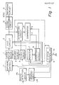
- Fig. l is a block diagram of an image pickup apparatus according to an embodiment of the present invention.
- the output of an image pickup device l in a video camera is connected to one input of an AGC circuit 2 for controlling a gain of an output signal from the image pickup device l.
- One input of the image pickup device l is connected to the output of clock driver circuit 3 for driving the image pickup device l.
- the input of the driver circuit 3 is connected to one output of a clock generator circuit 4 for generating a clock signal in accordance with a standard television format.
- the other output of the clock generator circuit 4 is connected to one input of an integrating circuit 5 for integrating a luminance signal supplied from the AGC circuit 2. Integration is performed in response to the clock signal from the clock generator circuit 4.
- the output of the integrating circuit 5 is connected to a comparator 6 for comparing the integrated result with two reference levels.
- a register 7 is connected to an operation circuit 8 (to be described later) to temporarily store gain data output from the operation circuit 8.
- the output of the register 7 is connected to the other input of the AGC circuit 2.
- a photo-detection device PS for a photometric purpose is arranged separately from the image pickup device l.
- the output of the photo-detection device PS is connected to a photometry circuit LM for calculating an object luminance on the basis of the outputs from the photo-detection device PS.
- the operation circuit 8 calculates gain data on the basis of the outputs from the comparator 6.
- a system controller 9 controls the overall operations of the image pickup system.
- a trigger switch l0 is connected between the system controller 9 and ground.
- a signal processing circuit l2 is connected to the AGC circuit 2, the integrating circuit 5, and a recording circuit l3.
- the signal processing circuit l2 receives a signal from the AGC circuit 2 and processes it to generate an NTSC signal or the like as a standard television signal.
- the NTSC signal is recorded in the recording circuit l3.
- the exposure control ll controls an amount of light incident on the image pickup device l on the basis of the exposure control data which is calculated on the basis of the output from the photometry circuit LM and sent from the system controller 9, so that the exposure control ll accumulates information signals (step #l02). Thereafter, the exposure control ll shields the image pickup device l in response to a control signal from the system controller 9 (step #l03). The information signal is then read out (#l04).
- a luminance signal in the information signal through the AGC circuit 2 is integrated by the integrating circuit 5 in response to the clock signal from the clock generator circuit 4 (#l05).
- the integrated result is compared by the comparator 6 with the reference levels. In other words, the comparator 6 determines whether the integration result falls within the predetermined range. More specifically, if the integrated result is less than a lowest threshold level Lmin, an output Ls from the comparator 6 is set at high (H) level. However, if the integrated result is higher than Lmax, an output Hs from the comparator 6 is set at high (H) level
- the gain of the AGC circuit 2 can be optimally controlled according to a two-threshold method (step #lll).
- both the outputs Hs and Ls are set at low level, i.e., when the output from the image pickup device l and hence the integrating circuit 5 falls within the range between Lmin and Lmax, i.e., the optimal range, the output gain is used as a gain G1. It should be noted that the operations in steps #l04 to #lll may be repeated. In this case, the flow returns from step #lll to step #l04 and does not advance to step #ll2.
- step #ll2 The same image information is then read out from the image pickup device l subjected to nondestructive read access (step #ll2).
- the exposure control ll shields the device l, and thus no changes in image information occur.
- the level of the readout image formation is controlled by the AGC circuit and falls within the dynamic range of the signal processing circuit l2.
- the ⁇ -correction and KNEE correction operations are performed at optimal operation timings.
- the processed image is recorded as a still image in the recording circuit l3.
- the read time of the output signal from the image pickup device l in a photometric operation may be shorter than that in the recording operation.
- the next exposure amount of the image pickup device l can be logarithmically regulated within the optimal range according to the two-threshold method. Therefore, the time required for optimizing the level of the output signal from the image pickup device l can be shortened.
- the total photometric time can be shortened, and thus the amount of incident light can be measured for a short period of time.
- a complicated mechanism is not required to fine-adjust the aperture or the like for exposure. Therefore, a compact video camera can be manufactured, and operability can be improved since only a photometric switch or the like is operated.
- a signal from an image pickup device having a wide dynamic range can be recorded at an optimal level.
- a user will not lose a shutter chance of a still image.
- the image pickup device output can be processed at the optimal operation timings, thereby properly reproducing gradation of the video image.
- the arrangement of the image pickup device l subjected nondestructive read access is shown in Fig. 3.
- the structure of the image pickup device l may be shown in, e.g., Japanese Patent Disclosure No. 12764/1985, and a detailed description thereof will be omitted.
- a reference photosensor cell 30 is indicated by a dotted circle.
- the collector of a bipolar transistor is connected to a semiconductor substrate and a semiconductor substrate electrode.
- the image pickup device l comprises: horizontal lines 3l, 3l ⁇ , 3l ⁇ ... for applying read and refresh pulses; a vertical shift register 32 for generating the read pulse, an interlacing circuit IL; buffer MOS transistors 33, 33 ⁇ , 33 ⁇ ...
- a terminal 34 for applying pulses to the gates of the buffer MOS transistors 33, 33 ⁇ , 33 ⁇ ...; buffer MOS transistors 35, 35 ⁇ , 35 ⁇ for applying refresh pulses; a terminal 36 for applying the refresh pulses to the gates of the transistors 35, 35 ⁇ , 35 ⁇ ...; a vertical shift register 52 for applying the refresh pulse; vertical lines 38, 38 ⁇ , 38 ⁇ ... and 5l, 5l ⁇ , 5l ⁇ ... for reading out an accumulated voltage from the reference photosensor cell 30; a horizontal shift register 39 for generating pulses for selecting each vertical line; gate MOS transistors 40, 40 ⁇ , 40 ⁇ ... and 49, 49 ⁇ , 49 ⁇ ...
- MOS transistors 42 and 53 for respectively refreshing the charges accumulated on the output lines 4l and 59 after the output lines 4l and 59 are accessed to read out the accumulated voltage to a sense amplifier; terminals 43 and 54 for respectively applying the refresh pulses to the MOS transistors 42 and 53; transistors 44 and 55 such as bipolar transistors, MOS-FETs, or J-FETs for amplifying the output signal; terminals 46 and 57 for respectively connecting load resistors 45 and 56 and the transistors 44 and 55 to a power source; transistor output terminals 47 and 58; MOS transistors 48, 48 ⁇ , 48 ⁇ ... and 50, 50 ⁇ , 50 ⁇ ... for refreshing the charges stored in the vertical lines 5l, 5l ⁇ , 5l ⁇ ... in the read mode; and a terminal l49 for applying pulses to the gates of the MOS transistors 48, 48 ⁇ , 48 ⁇ ... and 50, 50 ⁇ , 50 ⁇ ....
- a controller is constituted by the clock driver circuit 3 for supplying a drive pulse to the components 32, 34, 36, 39, 43, 49, 52, IL, and 54 and the clock generator circuit 4 for supplying timing pulses to the clock driver circuit 3.
- Fig. 4 is a block diagram of a signal processing system according to a second embodiment of the present invention.
- Level adjusters 200 and 300 are connected to the outputs of an image pickup device l to adjust signal gains of even-numbered fields in the nondestructive read mode.
- Switches SWl are selectively connected to the inputs (i.e., contacts a ) or outputs (i.e., contacts b ) of the level adjusters 200 and 300, respectively. More specifically, the switches SWl are set in the contact a positions for the odd-numbered fields and in the contact b positions for the even-numbered fields.
- a luminance processing circuit 500 is connected to a fixed contact c of one switch SWl to generate a luminance signal.
- a color processing circuit 600 is connected to a fixed contact c of the other switch SWl to generate color signals.
- the outputs of the luminance and color processing circuits 500 and 600 are connected to a process circuit 700.
- the process circuit 700 is designed to perform ⁇ -correction and AGC white balancing on the basis of the luminance and color signals to produce a luminance signal Y and color difference signals R-Y and B-Y.
- the outputs R-Y and B-Y of the process circuit 700 are connected to a magnetic recording circuit 800 and an encoder l000.
- the magnetic recording circuit 800 includes a color difference line sequential signal generator for converting the color difference simultaneous signals of the color difference signals R-Y and B-Y into line sequential signals, an FM modulator for FM-modulating the luminance and color difference line sequential signals, and a recording amplifier.
- a recording head 900 is connected to the output of the magnetic recording circuit 800 and is designed to record an FM signal to a video floppy disk (not shown).
- the encoder l000 generates an NTSC signal and supplies it to a VTR or the like.
- the NTSC signal is also supplied to and monitored by an EVF (Electronic View Finder) ll00.
- EVF Electronic View Finder
- a mode selection switch MSW is connected between a system controller and ground to select one of a still image recording (still) mode and a movie recording (movie) mode.
- a trigger release switch l0 is connected between the system controller 9 and ground to instruct photographing and recording.
- Fig. 5 is a chart for explaining driving of the image pickup apparatus under the control of the system controller.
- Column data nl, n2... are derived from the corresponding sensor cell columns.
- column data nl and n2 constitute data of the ol line
- column data n3 and n4 constitute data of the o2 line.
- combinations of the column data are changed. That is, column data n2 and n3 constitute data of the el line and column data n4 and n5 constitute data of the e2 line.
- the two horizontal line data as combinations each consisting of two lines shown in Fig. 5 are simultaneously read out in units of fields by the interlacing circuit IL.
- the readout data respectively appear at the output terminals 47 and 58.
- the image pickup system is controlled in the nondestructive read mode. Column data is not refreshed until the read operation for the even-numbered field is completed. Therefore, the identical data are read out first time in the odd-numbered field and second time in the even-numbered field.
- the image pickup device l is read-accessed in the nondestructive mode.
- the level of the output signal from the image pickup device l is reduced by several %. For this reason, the level of the output signal is compensated for a several % loss in the gain level adjusters 200 and 300.
- contacts b and c of the switches SWl are connected to each other since the control signal PSW from the system controller 9 is set at high level for a period (time t7 and time t8). Therefore, the even-numbered field signals having substantially the same level as that of the odd-numbered field signals are supplied to the luminance and color processing circuits 500 and 600. The processed signals are then recorded on the (n+l)th track.
- the magnetic recroding head 900 is then fed to the (n+2)th track. In this state, one-frame recording has been completed. Therefore, the magnetic recording head 900 waits for the next photographing cycle until the release switch l0 is depressed again.
- the signal levels in the odd- and even-numbered fields are set to be identical according to the number of read cycles, and thus a high-quality image free from flickering can be obtained.
- the shutter in the exposure control ll is kept open for a period (time tl to time t6) since the release switch l0 is kept on for this period.
- Row refreshing is performed upon read access of the corresponding row so as to set the nondestructive read mode.
- the system controller 9 outputs the pulse PSW of low level to connect the contacts a and b of the switches SWl.
- the clock driver 3 and the magnetic recording circuit 800 are operated for a period (time t2 to time t6).
- Fig. 7 is a timing chart of control pulses supplied from the clock driver circuit 3 to the image pickup device l shown in Fig. 4.
- a horizontal blanking pulse HBLK (A) is used as a reference pulse for explaining other pulses.
- Refresh pulses ⁇ H-RF (B) and ⁇ V-RF are respectively supplied to the shift register 52 and the terminal l49 within the horizontal blanking period.
- the charges accumulated in the bases of the sensor cells and the vertical lines are refreshed (grounded) through the transistors 48, 48 ⁇ , 48 ⁇ ... and 50, 50 ⁇ , 50 ⁇ ....
- a shift pulse ⁇ HS (D) is used for a horizontal shift register 39 and a shift pulse ⁇ VS (F) is used for a vertical shift register 32.
- a bit refresh pulse ⁇ HS-RF (E) is supplied to the terminals 43 and 54.
- the pulses that are associated with mode selections in the destructive or nondestructive mode are refresh pulses (B) and (C). In other words, when the refresh pulses are disabled, the nondestructive read mode is set.
- the system controller 9 controls the clock generator circuit 4 and the driver circuit 3 to arbitrarily select movie or still image recording.
- the pulses ⁇ H-RF and ⁇ V-RF are enabled to refresh the column data upon readout operation in units of horizontal blanking periods, as shown in Fig. 7.
- the pulses ⁇ H-RF and ⁇ V-RF are disabled to read out the same row signals in the odd- and even-numbered fields, i.e., two consecutive fields.
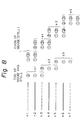
- Fig. 8 shows an image pickup system wherein three row outputs from an image pickup device are simultaneously read out.
- the arrangement of the image pickup device l in Fig. 8 can be easily modified from the two-line read arrangement of Fig. 3, and a detailed description thereof will be omitted.
- Column data nl, n2, and n3 constitute data of the ol line in the odd-numbered field
- column data n3, n4, and n5 constitute data of the o2 line in the even-numbered field. In this case, data of the odd-numbered field is nondestructively read out in the movie mode.
- column data n2, n3, and n4 constitute data of the el line
- column data n4, n5, and n6 constitute data of the e2 line.
- even-numbered row data is nondestructively read out in the movie mode. It should be noted that all row data are nondestructively read out in the still mode.
- the level of the output of only the uppermost line (i.e., odd-numbered row data) of the three row data (Fig. 8) constituting the ol, o2, and o3 lines is lowered.
- the level of the output of only the uppermost line (i.e., the even-numbered row data) of the three row data (Fig. 8) constituting the el, e2, and e3 lines is degraded in the same manner as described above.
- the levels of the outputs of upper two of the three row data constituting the el, e2, and e3 lines are lowered since these upper two row data are read out three times.
- the lowest row data is read out twice so that a decrease in level of the output is relatively small.
- Fig. 9 is a block diagram of a signal processing system of the embodiment shown in Fig. 8. This signal processing system is arranged by adding the following processing circuit to the embodiment of Fig. 4.
- the signal processing system in Fig. 9 additionally includes a multiplexer l0l.
- the multiplexer l0l is operated as follows.
- Output lines of row data nl, n2, n3... are connected such that row data nl, n4, n7... are connected to a first output terminal xl, that row data n2, n5, n8... are connected to a second output terminal x2, and that n3, n6, n9... are connected to a third output terminal x3.
- the multiplexer l0l connects the output terminals xl, x2, and x3 to the output terminals x4, x5, and x6, respectively.
- the output terminals x3, xl, and x2 are respectively connected to the output terminals x4, x5, and x6.
- the output terminals x2, x3, and xl are respectively connected to the output terminals x4, x5, and x6. In this manner, the connections of the output terminals xl to x3 and x4 to x6 are changed in units of horizontal lines.
- the multiplexer l0l connects the output terminals x2, x3, and xl, respectively, to the output terminals x4, x5, and x6.
- the multiplexer l0l connects the output terminals xl, x2, and x3, respectively, to the output terminals x4, x5, and x6.
- the multiplexer l0l connects the output terminals x3, xl, and x2, respectively to the output terminals x4, x5, and x6.
- the level of one of the outputs is different from those of the remaining outputs.
- the level different from those of the remaining outputs must be adjusted by the level adjusters 200 and 300.
- the output of the uppermost line of three outputs i.e., the output at the output terminal x4 (Fig. 9) is lowered.
- the level of the output at the terminal x4 is increased to match with those of the outputs at the output terminals x5 and x6.
- the level of the output of only the lowest line i.e., the output at the output terminal x6 is higher than those of the outputs appearing at the output terminals x4 and x5.
- the level of the output at the output terminal x6 is decreased by the level adjuster 300 to match with those of the outputs appearing at the output terminals x4 and x5.
- the system controller 9 controls to connect the contacts a and c in the movie mode and the contacts b and c in the still mode.
- Level adjusters 2l0, 220, and 230 are designed to increase the levels of the even-numbered field signals in the still mode. More specifically, as shown in Fig. 8, the second and third read cycles are performed for the even-numbered field, and the levels of the signals are greatly lowered, thus causing typical flickering. Since the level of the output appearing at the output terminal x6 is matched by the level adjuster 300 with those of the outputs at the output terminals x4 and x5. In the still mode, a difference of the outputs between the even- and odd-numbered fields is great. The flickering components are removed by the level adjusters 2l0, 220, and 230, thereby providing a high-quality image. Switches 450 are set such that contacts e and f thereof are connected to each other for both the odd-numbered field in the still mode and the movie mode and that contacts d and f thereof are connected to each other for the even-numbered fields in the still mode.
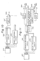
- Fig. l0 shows an arrangement wherein the level adjusters 2l0, 220, and 230 are simplified. Flickering is mainly caused by the luminance signal Y. For this reason, after the three-line outputs appearing at output terminals x4 ⁇ to x6 ⁇ are combined to obtain a composite signal and the luminance signal Y is generated according to the dot sequential processing of the three-line outputs, the level of the signal is adjusted by a level adjuster 2l0 ⁇ .
- a switch SW3 is set such that contacts c and e thereof are connected to each other for both the odd-numbered field in the still mode and the movie mode and that the contacts c and d thereof are connected to each other for the even-numbered field in the still mode.
- Another method of generating the luminance signal is proposed such that one of a plurality of outputs is processed as an output corresponding to a green filter and that the processed signal serves as a low-frequency luminance signal.
- the level adjuster is inserted in only the signal line for forming low-frequency luminance signal.
- Fig. ll shows a signal processing system wherein an output signal from the image pickup device is processed, and the level of the processed signal is adjusted according to a fifth embodiment of the present invention.
- the level of a luminance signal Y is adjusted by a level adjuster 2l0 ⁇ before the signal Y is input to a magnetic recording circuit 800.
- the levels of the outputs from the generating circuit 800 ⁇ are adjusted by a level adjuster 300 ⁇ .
- Switches SW4 and SW5 are set such that contacts a and c thereof are connected to each other for the even-numbered field in the still mode and that contacts b and c thereof are connected to each other for both the odd-numbered field in the still mode and the movie mode.
- the signal level is adjusted according to the number of read cycles. Therefore, the flickering components of the luminance signal, the deviations in color components, deviations in white balance, and color flickering can be completely eliminated. Therefore, the advantageous feature of the nondestructive read access type image pickup system can be maximized.
- the nondestructive and destructive read modes are selectively switched, and thus the movie or still image can be selected in accordance with the photographing purpose.
- the photographing conditions prior to still image recording can be checked without flickering.
- the gain of the output from the image pickup system is adjusted according to the number of read cycles when the output is repeatedly read out from the nondestructive read access type image pickup system a plurality of times. Therefore, flickering can be eliminated to greatly improve image quality.
Landscapes
- Engineering & Computer Science (AREA)
- Multimedia (AREA)
- Signal Processing (AREA)
- Transforming Light Signals Into Electric Signals (AREA)
- Apparatus For Radiation Diagnosis (AREA)
- Vehicle Body Suspensions (AREA)
- Photographic Developing Apparatuses (AREA)
- Facsimile Scanning Arrangements (AREA)
Applications Claiming Priority (4)
| Application Number | Priority Date | Filing Date | Title |
|---|---|---|---|
| JP61093982A JPH0642721B2 (ja) | 1986-04-23 | 1986-04-23 | 撮像方式 |
| JP93982/86 | 1986-04-23 | ||
| JP174981/86 | 1986-07-25 | ||
| JP61174981A JPH0642722B2 (ja) | 1986-07-25 | 1986-07-25 | 撮像装置 |
Publications (3)
| Publication Number | Publication Date |
|---|---|
| EP0243157A2 true EP0243157A2 (de) | 1987-10-28 |
| EP0243157A3 EP0243157A3 (en) | 1989-03-01 |
| EP0243157B1 EP0243157B1 (de) | 1994-09-07 |
Family
ID=26435249
Family Applications (1)
| Application Number | Title | Priority Date | Filing Date |
|---|---|---|---|
| EP87303515A Expired - Lifetime EP0243157B1 (de) | 1986-04-23 | 1987-04-22 | Bildaufnahmegerät |
Country Status (4)
| Country | Link |
|---|---|
| US (1) | US4779137A (de) |
| EP (1) | EP0243157B1 (de) |
| AT (1) | ATE111281T1 (de) |
| DE (1) | DE3750487D1 (de) |
Cited By (2)
| Publication number | Priority date | Publication date | Assignee | Title |
|---|---|---|---|---|
| FR2696610A1 (fr) * | 1992-09-29 | 1994-04-08 | Mitsubishi Electric Corp | Dispositif de traitement de signaux pour un élément de formation d'images à l'état solide. |
| EP0619673A1 (de) * | 1993-04-09 | 1994-10-12 | Sony Corporation | Bildsensor und elektronische Stehbildkamera |
Families Citing this family (16)
| Publication number | Priority date | Publication date | Assignee | Title |
|---|---|---|---|---|
| JPH0258981A (ja) * | 1988-08-24 | 1990-02-28 | Nikon Corp | 電子スチルカメラ |
| EP0372514B1 (de) * | 1988-12-06 | 1997-03-05 | Canon Kabushiki Kaisha | Bildaufnahmesystem |
| US5258845A (en) * | 1989-05-19 | 1993-11-02 | Canon Kabushiki Kaisha | Solid-state image sensor driving device with signal synthesizing |
| KR970003032B1 (ko) * | 1989-10-17 | 1997-03-13 | 상요 덴기 가부시끼가이샤 | 고체 촬상 장치 |
| US5138458A (en) * | 1989-12-22 | 1992-08-11 | Olympus Optical Co., Ltd. | Electronic camera apparatus capable of providing wide dynamic range image signal |
| JPH0474077A (ja) * | 1990-07-13 | 1992-03-09 | Matsushita Electric Ind Co Ltd | 画像記録装置 |
| US5288988A (en) * | 1990-08-07 | 1994-02-22 | Canon Kabushiki Kaisha | Photoconversion device having reset control circuitry |
| US5264940A (en) * | 1990-10-08 | 1993-11-23 | Olympus Optical Co., Ltd. | Image sensing apparatus having exposure level and dynamic range control circuit |
| US5262873A (en) * | 1990-11-07 | 1993-11-16 | Canon Kabushiki Kaisha | Image signal correcting in image data processing requiring only small memory capacity |
| JP3617857B2 (ja) * | 1995-04-17 | 2005-02-09 | 株式会社東芝 | カラー撮像装置 |
| JPH10136244A (ja) * | 1996-11-01 | 1998-05-22 | Olympus Optical Co Ltd | 電子的撮像装置 |
| US6930710B1 (en) * | 1998-11-13 | 2005-08-16 | Cnh Canada, Ltd. | Method of and apparatus for processing a video image |
| JP4205932B2 (ja) * | 2002-11-19 | 2009-01-07 | アルプス電気株式会社 | 照明装置及び液晶表示装置 |
| US8687087B2 (en) | 2006-08-29 | 2014-04-01 | Csr Technology Inc. | Digital camera with selectively increased dynamic range by control of parameters during image acquisition |
| US7714903B2 (en) * | 2006-08-29 | 2010-05-11 | Zoran Corporation | Wide dynamic range image capturing system method and apparatus |
| JP5040960B2 (ja) * | 2009-06-04 | 2012-10-03 | 株式会社ニコン | 電子カメラ |
Family Cites Families (8)
| Publication number | Priority date | Publication date | Assignee | Title |
|---|---|---|---|---|
| GB1437328A (en) * | 1972-09-25 | 1976-05-26 | Rca Corp | Sensors having recycling means |
| JPS5795777A (en) * | 1980-12-05 | 1982-06-14 | Fuji Photo Film Co Ltd | Video recorder |
| US4603354A (en) * | 1982-06-09 | 1986-07-29 | Canon Kabushiki Kaisha | Image pickup device |
| US4525741A (en) * | 1982-11-03 | 1985-06-25 | Ncr Corporation | Self-adjusting video camera |
| JPS6038988A (ja) * | 1983-08-12 | 1985-02-28 | Victor Co Of Japan Ltd | 固体撮像素子を用いた静止画像撮像装置 |
| JPS6058780A (ja) * | 1983-09-09 | 1985-04-04 | Olympus Optical Co Ltd | 測光機能を備えた固体撮像装置 |
| GB2170374B (en) * | 1984-12-28 | 1989-04-05 | Canon Kk | Image sensing apparatus |
| US4731665A (en) * | 1984-12-28 | 1988-03-15 | Canon Kabushiki Kaisha | Image sensing apparatus with read-out of selected combinations of lines |
-
1987
- 1987-04-17 US US07/039,288 patent/US4779137A/en not_active Expired - Lifetime
- 1987-04-22 DE DE3750487T patent/DE3750487D1/de not_active Expired - Lifetime
- 1987-04-22 EP EP87303515A patent/EP0243157B1/de not_active Expired - Lifetime
- 1987-04-22 AT AT87303515T patent/ATE111281T1/de active
Non-Patent Citations (1)
| Title |
|---|
| None |
Cited By (3)
| Publication number | Priority date | Publication date | Assignee | Title |
|---|---|---|---|---|
| FR2696610A1 (fr) * | 1992-09-29 | 1994-04-08 | Mitsubishi Electric Corp | Dispositif de traitement de signaux pour un élément de formation d'images à l'état solide. |
| US5483281A (en) * | 1992-09-29 | 1996-01-09 | Mitsubishi Denki Kabushiki Kaisha | Signal processing device for a two-dimensional solid-state imaging element |
| EP0619673A1 (de) * | 1993-04-09 | 1994-10-12 | Sony Corporation | Bildsensor und elektronische Stehbildkamera |
Also Published As
| Publication number | Publication date |
|---|---|
| ATE111281T1 (de) | 1994-09-15 |
| US4779137A (en) | 1988-10-18 |
| DE3750487D1 (de) | 1994-10-13 |
| EP0243157B1 (de) | 1994-09-07 |
| EP0243157A3 (en) | 1989-03-01 |
Similar Documents
| Publication | Publication Date | Title |
|---|---|---|
| US4779137A (en) | Image pickup apparatus | |
| US10506188B2 (en) | Solid-state imaging device | |
| USRE42974E1 (en) | CMOS active pixel sensor type imaging system on a chip | |
| US7369166B2 (en) | Single substrate camera device with CMOS image sensor | |
| US9214491B2 (en) | Solid-state imaging apparatus for causing an FD capacitor value to be variable without increasing a number of elements | |
| JP5106052B2 (ja) | 固体撮像素子、撮像システム、及び固体撮像素子の駆動方法 | |
| US7456886B2 (en) | Image pickup apparatus | |
| US5841126A (en) | CMOS active pixel sensor type imaging system on a chip | |
| US8547463B2 (en) | Solid-state imaging device and control method for same | |
| US6930722B1 (en) | Amplification type image pickup apparatus and method of controlling the amplification type image pickup apparatus | |
| US8384804B2 (en) | Imaging apparatus for processing noise signal and photoelectric conversion signal | |
| US5528291A (en) | CCD image pickup device and method of driving which maintains sensitivity regardless of the operating mode | |
| KR20090091314A (ko) | 고체 촬상 장치, 고체 촬상 장치의 구동 방법 및 촬상 장치 | |
| US6975357B1 (en) | Solid-state imaging pickup device with vertical and horizontal driving means for a unit pixel | |
| US20050195307A1 (en) | Image pickup apparatus including a plurailty of pixels, each having a photoelectric conversion element and an amplifier whose output is prevented from falling below a predetermined level | |
| US7973843B2 (en) | Active pixel sensor with reduced fixed pattern noise | |
| US8149308B2 (en) | Solid-state image pickup device | |
| JP2025166790A (ja) | イメージセンサ | |
| USRE42918E1 (en) | Single substrate camera device with CMOS image sensor | |
| JP2791999B2 (ja) | 固体撮像装置の駆動方法と固体撮像装置 | |
| JPS6331376A (ja) | 撮像装置 | |
| WO2025192176A1 (ja) | 撮像素子および電子機器 | |
| JPS6331377A (ja) | 撮像装置 | |
| JP2019009820A (ja) | 固体撮像素子 |
Legal Events
| Date | Code | Title | Description |
|---|---|---|---|
| PUAI | Public reference made under article 153(3) epc to a published international application that has entered the european phase |
Free format text: ORIGINAL CODE: 0009012 |
|
| AK | Designated contracting states |
Kind code of ref document: A2 Designated state(s): AT BE CH DE ES FR GB GR IT LI LU NL SE |
|
| PUAL | Search report despatched |
Free format text: ORIGINAL CODE: 0009013 |
|
| AK | Designated contracting states |
Kind code of ref document: A3 Designated state(s): AT BE CH DE ES FR GB GR IT LI LU NL SE |
|
| 17P | Request for examination filed |
Effective date: 19890719 |
|
| 17Q | First examination report despatched |
Effective date: 19910225 |
|
| GRAA | (expected) grant |
Free format text: ORIGINAL CODE: 0009210 |
|
| AK | Designated contracting states |
Kind code of ref document: B1 Designated state(s): AT BE CH DE ES FR GB GR IT LI LU NL SE |
|
| PG25 | Lapsed in a contracting state [announced via postgrant information from national office to epo] |
Ref country code: IT Free format text: LAPSE BECAUSE OF FAILURE TO SUBMIT A TRANSLATION OF THE DESCRIPTION OR TO PAY THE FEE WITHIN THE PRE;WARNING: LAPSES OF ITALIAN PATENTS WITH EFFECTIVE DATE BEFORE 2007 MAY HAVE OCCURRED AT ANY TIME BEFORE 2007. THE CORRECT EFFECTIVE DATE MAY BE DIFFERENT FROM THE ONE RECORDED.SCRIBED TIME-LIMIT Effective date: 19940907 Ref country code: AT Effective date: 19940907 Ref country code: NL Effective date: 19940907 Ref country code: GR Free format text: LAPSE BECAUSE OF FAILURE TO SUBMIT A TRANSLATION OF THE DESCRIPTION OR TO PAY THE FEE WITHIN THE PRESCRIBED TIME-LIMIT Effective date: 19940907 Ref country code: BE Effective date: 19940907 Ref country code: CH Effective date: 19940907 Ref country code: LI Effective date: 19940907 |
|
| REF | Corresponds to: |
Ref document number: 111281 Country of ref document: AT Date of ref document: 19940915 Kind code of ref document: T |
|
| REF | Corresponds to: |
Ref document number: 3750487 Country of ref document: DE Date of ref document: 19941013 |
|
| ET | Fr: translation filed | ||
| PG25 | Lapsed in a contracting state [announced via postgrant information from national office to epo] |
Ref country code: SE Effective date: 19941207 |
|
| PG25 | Lapsed in a contracting state [announced via postgrant information from national office to epo] |
Ref country code: DE Effective date: 19941208 |
|
| REG | Reference to a national code |
Ref country code: CH Ref legal event code: PL |
|
| PG25 | Lapsed in a contracting state [announced via postgrant information from national office to epo] |
Ref country code: ES Free format text: LAPSE BECAUSE OF FAILURE TO SUBMIT A TRANSLATION OF THE DESCRIPTION OR TO PAY THE FEE WITHIN THE PRESCRIBED TIME-LIMIT Effective date: 19941218 |
|
| NLV1 | Nl: lapsed or annulled due to failure to fulfill the requirements of art. 29p and 29m of the patents act | ||
| PG25 | Lapsed in a contracting state [announced via postgrant information from national office to epo] |
Ref country code: LU Free format text: LAPSE BECAUSE OF NON-PAYMENT OF DUE FEES Effective date: 19950430 |
|
| PLBE | No opposition filed within time limit |
Free format text: ORIGINAL CODE: 0009261 |
|
| STAA | Information on the status of an ep patent application or granted ep patent |
Free format text: STATUS: NO OPPOSITION FILED WITHIN TIME LIMIT |
|
| 26N | No opposition filed | ||
| REG | Reference to a national code |
Ref country code: GB Ref legal event code: IF02 |
|
| PGFP | Annual fee paid to national office [announced via postgrant information from national office to epo] |
Ref country code: GB Payment date: 20060418 Year of fee payment: 20 |
|
| PGFP | Annual fee paid to national office [announced via postgrant information from national office to epo] |
Ref country code: FR Payment date: 20060426 Year of fee payment: 20 |
|
| REG | Reference to a national code |
Ref country code: GB Ref legal event code: PE20 |
|
| PG25 | Lapsed in a contracting state [announced via postgrant information from national office to epo] |
Ref country code: GB Free format text: LAPSE BECAUSE OF EXPIRATION OF PROTECTION Effective date: 20070421 |